Semiconductor devices with graded dopant regions
US20160172447A1
2016-06-16
14/931,636
2015-11-03
✅ Patent granted
US 9,647,070 B2
2017-05-09
-
-
Ajay K Arora
Howison and Arnott, LLP
2035-11-03
Abstract:
Most semiconductor devices manufactured today, have uniform dopant concentration, either in the lateral or vertical device active (and isolation) regions. By grading the dopant concentration, the performance in various semiconductor devices can be significantly improved.
Performance improvements can be obtained in application specific areas like increase in frequency of operation for digital logic, various power MOSFET and IGBT ICS, improvement in refresh time for DRAM's, decrease in programming time for nonvolatile memory, better visual quality including pixel resolution and color sensitivity for imaging ICs, better sensitivity for varactors in tunable filters, higher drive capabilities for JFET's, and a host of other applications.
Inventors:
- G. R. Mohan Rao 19 🇺🇸 Allen, TX, United States
- G.R. Mohan Rao 19 🇺🇸 Allen, TX, United States
Assignee:
- GREENTHREAD, LLC 9 🇺🇸 Dallas, TX, United States
Applicant:
Interested in similar patents?
Get notified when new applications in this technology area are published.
Classification:
H01L29/1095 » CPC main
Semiconductor devices adapted for rectifying, amplifying, oscillating or switching, or capacitors or resistors with at least one potential-jump barrier or surface barrier, e.g. PN junction depletion layer or carrier concentration layer; Details of semiconductor bodies or of electrodes thereof; Multistep manufacturing processes therefor; Semiconductor bodies ; Multistep manufacturing processes therefor characterised by their shape; characterised by the shapes, relative sizes, or dispositions of the semiconductor regions ; characterised by the concentration or distribution of impurities within semiconductor regions with semiconductor regions connected to an electrode not carrying current to be rectified, amplified or switched and such electrode being part of a semiconductor device which comprises three or more electrodes Body region, i.e. base region, of DMOS transistors or IGBTs
H01L29/10 IPC
Semiconductor devices adapted for rectifying, amplifying, oscillating or switching, or capacitors or resistors with at least one potential-jump barrier or surface barrier, e.g. PN junction depletion layer or carrier concentration layer; Details of semiconductor bodies or of electrodes thereof; Multistep manufacturing processes therefor; Semiconductor bodies ; Multistep manufacturing processes therefor characterised by their shape; characterised by the shapes, relative sizes, or dispositions of the semiconductor regions ; characterised by the concentration or distribution of impurities within semiconductor regions with semiconductor regions connected to an electrode not carrying current to be rectified, amplified or switched and such electrode being part of a semiconductor device which comprises three or more electrodes
H01L29/739 IPC
Semiconductor devices adapted for rectifying, amplifying, oscillating or switching, or capacitors or resistors with at least one potential-jump barrier or surface barrier, e.g. PN junction depletion layer or carrier concentration layer; Details of semiconductor bodies or of electrodes thereof; Multistep manufacturing processes therefor; Types of semiconductor device ; Multistep manufacturing processes therefor controllable by only the electric current supplied, or only the electric potential applied, to an electrode which does not carry the current to be rectified, amplified or switched; Bipolar devices; Transistor-type devices, i.e. able to continuously respond to applied control signals controlled by field-effect, e.g. bipolar static induction transistors [BSIT]
H01L27/14643 » CPC further
Devices consisting of a plurality of semiconductor or other solid-state components formed in or on a common substrate including semiconductor components sensitive to infra-red radiation, light, electromagnetic radiation of shorter wavelength or corpuscular radiation and specially adapted either for the conversion of the energy of such radiation into electrical energy or for the control of electrical energy by such radiation; Devices controlled by radiation; Imager structures Photodiode arrays; MOS imagers
H01L29/36 » CPC further
Semiconductor devices adapted for rectifying, amplifying, oscillating or switching, or capacitors or resistors with at least one potential-jump barrier or surface barrier, e.g. PN junction depletion layer or carrier concentration layer; Details of semiconductor bodies or of electrodes thereof; Multistep manufacturing processes therefor; Semiconductor bodies ; Multistep manufacturing processes therefor characterised by the concentration or distribution of impurities in the bulk material
H01L27/0214 » CPC further
Devices consisting of a plurality of semiconductor or other solid-state components formed in or on a common substrate including semiconductor components specially adapted for rectifying, oscillating, amplifying or switching and having at least one potential-jump barrier or surface barrier; including integrated passive circuit elements with at least one potential-jump barrier or surface barrier; Particular design considerations for integrated circuits for internal polarisation, e.g. I2L
H01L27/10844 » CPC further
Devices consisting of a plurality of semiconductor or other solid-state components formed in or on a common substrate including semiconductor components specially adapted for rectifying, oscillating, amplifying or switching and having at least one potential-jump barrier or surface barrier; including integrated passive circuit elements with at least one potential-jump barrier or surface barrier the substrate being a semiconductor body including a plurality of individual components in a repetitive configuration including field-effect components; Dynamic random access memory structures Multistep manufacturing methods
H01L21/02 IPC
Processes or apparatus adapted for the manufacture or treatment of semiconductor or solid state devices or of parts thereof Manufacture or treatment of semiconductor devices or of parts thereof
H01L27/146 IPC
Devices consisting of a plurality of semiconductor or other solid-state components formed in or on a common substrate including semiconductor components sensitive to infra-red radiation, light, electromagnetic radiation of shorter wavelength or corpuscular radiation and specially adapted either for the conversion of the energy of such radiation into electrical energy or for the control of electrical energy by such radiation; Devices controlled by radiation Imager structures
H01L27/02 IPC
Devices consisting of a plurality of semiconductor or other solid-state components formed in or on a common substrate including semiconductor components specially adapted for rectifying, oscillating, amplifying or switching and having at least one potential-jump barrier or surface barrier; including integrated passive circuit elements with at least one potential-jump barrier or surface barrier
H01L27/108 IPC
Devices consisting of a plurality of semiconductor or other solid-state components formed in or on a common substrate including semiconductor components specially adapted for rectifying, oscillating, amplifying or switching and having at least one potential-jump barrier or surface barrier; including integrated passive circuit elements with at least one potential-jump barrier or surface barrier the substrate being a semiconductor body including a plurality of individual components in a repetitive configuration including field-effect components Dynamic random access memory structures
Description
CROSS-REFERENCE TO RELATED APPLICATIONS
This application is a Continuation of U.S. patent application Ser. No. 14/515,584, filed Oct. 16, 2014, published on Feb. 5, 2015, as U.S. Publication No. 2015-0035004, now U.S. Pat. No. 9,190,502, issued on Nov. 17, 2015, (GRTD-32613). Application Ser. No. 14/515,584 is a Continuation of U.S. patent application Ser. No. 13/854,319 filed Apr. 1, 2013, published on Aug. 29, 2013, as U.S. Publication No. 2013-0221488 (GRTD-32626). Application Ser. No. 13/854,319 is a Continuation of Ser. No. 11/622,496, filed Jan. 12, 2007, published on Jul. 12, 2007, as Publication No. 2007-0158790, now U.S. Pat. No. 8,421,195, issued on Apr. 16, 2013 (GRTD-32611). Application Ser. No. 11/622,496, is a Division of U.S. patent application Ser. No. 10/934,915, filed Sep. 3, 2004, published on Mar. 9, 2006, as U.S. Publication No. 2006-0049464 (GRTD-32625). U.S. Pat. Nos. 9,190,502, and 8,421,195, and Patent Application Publication Nos. 2015-0035004, 2013-0221488, 2007-0158790, and 2006-0049464, are incorporated herein by reference in their entirety.
TECHNICAL FIELD
This present invention relates to all semiconductor devices and systems. Particularly it applies to diffused diodes, avalanche diodes, Schottky devices, power MOS transistors, JFETs, RF bipolar transistors, IGBTs (Insulated Gate Bipolar Transistors), varactors, digital VLSI, mixed signal circuits and sensor devices including camera ICs employing CCD (Charge Coupled Device) as well as CMOS technologies.
BACKGROUND
Bipolar Junction transistors (BJT) are minority carrier devices as the principle device conduction mechanism. However, majority carriers also a small yet finite role in modulating the conductivity in BJTs. Consequently, both carriers (electrons and holes) play a role in the switching performance of BJTs. The maximum frequency of operation in BJTs is limited by the base transit time as well as the quick recombination of the majority carriers when the device is switched off (prior to beginning the next cycle). The dominant carrier mechanism in BJTs is carrier diffusion. Carrier drift current component is fairly small, especially in uniformly doped base BJTs. Efforts have been made in graded base transistors to create an ‘aiding drift field’, to enhance the diffusing minority carrier's speed from emitter to collector. However, most semiconductor devices, including various power MOSFETs (traditional, DMOS, lateral, vertical and a host of other configurations), IGBT's (Insulated Gated Base Transistors), still use a uniformly doped ‘drift epitaxial’ region in the base. FIG. 1 shows the relative doping concentration versus distance in a BJT. FIG. 2 shows the ‘uniformly doped epi region’ in a IGBT. In contrast to BJTs, MOS devices are majority carrier devices for conduction. The conduction is channel dominated. The channel can be a surface in one plane in planar devices. The surface can also be on the sidewalls in a vertical device. Other device architectures to combine planar and vertical conductions are also possible. The maximum frequency of operation is dictated primarily by source-drain separation distance. Most MOS devices use a uniformly doped substrate (or a well region). When a MOSFET is optimillay integrated with a BJT in a monolithic fashion, an IGBT results. The IGBT inherits the advantages of both MOSFET and BJT. It also brings new challenges because the required characteristics (electron transit and hole recombination as fast as possible in the case of an n-channel IGBT) require different dopant gradients either in the same layer at different positions, or at the interfaces of similar or dissimilar layers.
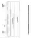
‘Retrograde’ wells have been attempted, with little success, to help improve soft error immunity in SRAM's and visual quality in imaging circuits. FIG. 3(a) shows a typical CMOS VLSI device employing a twin well substrate, on which active devices are subsequently fabricated. FIGS. 3(b), 3(c), and 3(d) illustrate device cross sections, as practiced today. ‘Retrograde’ and ‘halo’ wells have also been attempted to improve refresh time in DRAM's (dynamic random access memories), as well as, reducing dark current (background noise) and enhance RGB (Red, Green, Blue) color resolution in digital camera Ics. Most of these techniques either divert the minority carriers away form the active regions of critical charge storage nodes at the surface, or, increase minority carrier density locally as the particular application requires.
BRIEF DESCRIPTION OF THE DRAWINGS
For a more complete understanding of the present invention, and the advantages thereof, reference is now made to the following descriptions taken in conjunction with the accompanying drawings, in which:
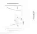
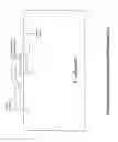
FIG. 1 illustrates the relative doping profiles of emitter, base, and collector, for the two most popular bipolar junction transistors: namely, A—uniform base, and B—graded base;
FIG. 2 illustrates the cross section of a commercial IGBT with a uniform epitaxial drift region (base);
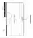
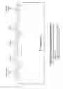
FIGS. 3(a), 3(b), 3(c), 3(d) illustrate cross sections commonly used CMOS silicon substrate with two wells (one n-well in which p-channel transistors are subsequently fabricated, and, one p-well in which n-channel transistors are subsequently fabricated)—typical IC, EEPROM using tunnel insulator, DRAM and NAND flash;
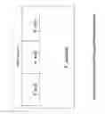
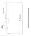
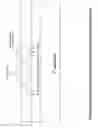
FIG. 4 illustrates the cross section of a IGBT, using one embodiment of the invention described here, where the dopant is optimally graded in the epitaxial drift region; and
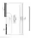
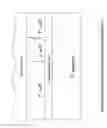
FIGS. 5(a), 5(b), 5(c) illustrate the cross sections of a MOS silicon substrate with two wells, and, an underlying layer using embodiments of the invention to improve performance in each application—VLSI logic, DRAM/image IC, nonvolatile memory IC.
DETAILED DESCRIPTION
The relative doping concentrations of emitter and collector regions varies from 1018 to 1020/cm3, where as the base region is 1014 to 1016/cm3 depending on the desired characteristics of the BJT. In graded base p-n-p transistors, the donor dopant concentration may be 10 to 100× at the emitter-base junction, relative to the base-collector junction (1×). The gradient can be linear, quasi linear, exponential or complimentary error function. The relative slope of the donor concentration throughout the base, creates a suitable aiding drift electric field, to help the holes (p-n-p transistor) transverse from emitter to collector. Since the aiding drift field helps hole conduction, the current gain at a given frequency is enhanced, relative to a uniformly-doped-(base) BJT. The improvement in cut-off frequency (or, frequency at unity gain, fT) can be as large as 2×-5×. Similar performance improvements are also applicable to n-p-n transistors.
As illustrated in FIG. 4, in one embodiment according to the invention, a donor gradient is established from the emitter-drift epitaxial base region junction of the punch-through IGBT, to the drift epitaxial base region—nt buffer layer boundary (electrons in this case are accelerated in their transit from emitter to collector). The ‘average’ base resistance is optimized, so that conductivity modulation and lifetime (for minority carriers) in base region are not compromised. By sweeping the carriers towards the nt buffer region two advantages are obtained—the frequency of operation (combination of ton and toff as is known in the IGBT commercial nomenclature) can be enhanced. More importantly, during toff, holes can be recombined much quicker at the nt buffer layer, compared to a uniformly doped n− epitaxial drift region by establishing a different dopant gradient near the n+ buffer layer. It should be noted that the drift region can also be a non-epitaxial silicon substrate. Epitaxy enhances lifetime, but, epitaxy is not mandatory. Different layers of dopant regions can be transferred through wafer to wafer bonding (or other similar transfer mechanisms) for eventual device fabrication. The “reverse recovery time” for an IGBT is significantly improved due to the optimized graded dopant in the so called “drift region” as well as at the interfaces of the drift region. Graded dopants can also be implemented in the n+ buffer layer as well as other regions adjacent to the respective layers. Two important performance enhancements are the result of dopant gradients. For example, in an n-channel IGBT, electrons can be swept from source to drain rapidly, while at same time holes can be recombined closer to the n+ buffer layer. This can improve t(on) and t(off) in the same device.
As illustrated in FIGS. 5(a), 5(b), 5(c), donor gradient is also of benefit to very large scale integrated circuits (VLSI)—VLSI logic, DRAM, nonvolatile memory like NAND flash. Spurious minority carriers can be generated by clock switching in digital VLSI logic and memory IC'S. These unwanted carriers can discharge dynamically-held ‘actively held high’ nodes. Statically held nodes (with Vcc) can not be affected, in most cases. Degradation of refresh time in DRAM's is one of the results, because the capacitor holds charge dynamically. Similarly, degradation of CMOS digital images, in digital imaging IC's is another result of the havoc caused by minority carriers. Pixel and color resolution can be significantly enhanced in imaging IC's with the embodiments described here. Creating ‘Sub Terrain’ recombination centers underneath the wells (gold doping, platinum doping) as is done in some high-voltage diodes is not practical for VLSI circuits. Hence, a novel technique has been described here by creating a drift field to sweep these unwanted minority carriers into the substrate as quickly as possible, from the active circuitry at the surface. In a preferred embodiment, the subterrain n-layer has a graded donor concentration to sweep the minority carriers deep into the substrate. One or more of such layers can also be implemented through wafer to wafer bonding or similar “transfer” mechanisms. This n-layer can be a deeply-implanted layer. It can also be an epitaxial layer. The n-well and p-well also can be graded or retrograded in dopants, as desired, to sweep those carriers away from the surface as well. The graded dopant can also be implemented in surface channel MOS devices to accelerate majority carriers towards the drain. In nonvolatile memory devices, to decrease programming time, carriers should be accelerated towards the surface when programming of memory cells is executed. The graded dopant can also be used to fabricate superior Junction field-effect transistors where the “channel pinchoff” is controlled by a graded channel instead of a uniformly doped channel (as practiced in prior art).
One of ordinary skill and familiarity in the art will recognize that the concepts taught herein can be customized and tailored to a particular application in many advantageous ways. For instance, minority carriers can be channeled to the surface, to aid programming in nonvolatile memory devices (NOR, NAND, multivalued-cell). Moreover, single well, as well triple-well CMOS fabrication techniques can also be optimized to incorporate these embodiments, individually and collectively. Any modifications of such embodiments (described here) fall within the spirit and scope of the invention. Hence, they fall within the scope of the claims described below
Although the invention has been described with reference to specific embodiments, these descriptions are not meant to be construed in a limiting sense. Various modifications of the disclosed embodiments, as well as alternative embodiments of the invention will become apparent to persons skilled in the art upon reference to the description of the invention. It should be appreciated by those skilled in the art that the conception and the specific embodiment disclosed may be readily utilized as a basis for modifying or designing other structures for carrying out the same purposes of the present invention. It should also be realized by those skilled in the art that such equivalent constructions do not depart from the spirit and scope of the invention as set forth in the appended claims.
It is therefore, contemplated that the claims will cover any such modifications or embodiments that fall within the true scope of the invention.
Claims
What is claimed is:1. A semiconductor device with graded dopant concentration in the active region, to aid carrier movement from emitter to collector.
Images & Drawings included:
Sources:
- United States Patent and Trademark Office - verify current appl. status at the USPTO↗
Similar patent applications:
- » 20060049464
Semiconductor devices with graded dopant regions - » 20070158790
Semiconductor devices with graded dopant regions - » 20100006138
Semiconductor devices with graded dopant regions - » 20130221488
SEMICONDUCTOR DEVICES WITH GRADED DOPANT REGIONS - » 20150035004
Semiconductor devices with graded dopant regions - » 20170243876
Semiconductor devices with graded dopant regions - » 20200127095
Semiconductor devices with graded dopant regions - » 20210005716
Semiconductor devices with graded dopant regions - » 20210359086
Semiconductor devices with graded dopant regions - » 20220246725
SEMICONDUCTOR DEVICES WITH GRADED DOPANT REGIONS
Recent applications in this class:
- » 20240363691 2024-10-31
WIDE BANDGAP MATERIAL IN DRIFT WELL OF SEMICONDUCTOR DEVICE - » 20240304672 2024-09-12
TRANSISTOR STRUCTURE WITH MULTIPLE VERTICAL THIN BODIES - » 20240266401 2024-08-08
TRANSISTOR DEVICE AND MANUFACTURING METHOD THEREOF - » 20240266400 2024-08-08
SEMICONDUCTOR DEVICE AND METHOD FOR MANUFACTURING THE SAME - » 20240153999 2024-05-09
SEMICONDUCTOR DEVICE AND METHOD OF FABRICATING THE SAME - » 20240128323 2024-04-18
METAL OXIDE SEMICONDUCTOR FIELD EFFECT TRANSISTORS (MOSFET) INCLUDING DEEP P-WELLS AND METHODS OF FORMING SAME - » 20240120384 2024-04-11
SIC SEMICONDUCTOR DEVICE - » 20240096965 2024-03-21
SEMICONDUCTOR DEVICE - » 20240088230 2024-03-14
SEMICONDUCTOR DEVICE AND METHOD FOR MANUFACTURING SAME - » 20240063267 2024-02-22
SEMICONDUCTOR DEVICE AND METHOD FOR PRODUCING SAME
Recent applications for this Assignee:
- » 20210359086 2021-11-18
Semiconductor devices with graded dopant regions - » 20210005716 2021-01-07
Semiconductor devices with graded dopant regions - » 20200127095 2020-04-23
Semiconductor devices with graded dopant regions - » 20170243876 2017-08-24
Semiconductor devices with graded dopant regions - » 20160155496 2016-06-02
Lifetime mixed level non-volatile memory system - » 20150278013 2015-10-01
Lifetime mixed level non-volatile memory system - » 20150070991 2015-03-12
Nonvolatile memory systems with embedded fast read and write memories - » 20150035004 2015-02-05
Semiconductor devices with graded dopant regions