Semiconductor light emitting diode chip with current extension layer and graphical current extension layers
US20160247989A1
2016-08-25
15/026,020
2014-03-13
✅ Patent granted
US 9,666,779 B2
2017-05-30
WO; PCT/CN2014/073361; 20140313
WO; WO2015/074353; 20150528
Matthew Landau | Grant Withers
The Webb Law Firm
2034-03-13
Abstract:
A semiconductor light emitting diode chip relates to the field of production technologies of a light emitting diode. In the present invention, corresponding graphical current extension layers are respectively disposed below an N pad and a P pad, and in all light emitting compound areas, there is electronic compound light emitting. Compared with the prior art, an area of a light emitting compound area is increased, which can effectively improve current distribution and light emitting brightness of a chip. In addition, graphical current extension can effectively increase an adhesion of a pad on a surface and improve the reliability of a chip.
Inventors:
- Yuzhe Jin 1 🇨🇳 Yangzhou City, China
- Yaping Feng 1 🇨🇳 Yangzhou City, China
- Yi Zhang 1 🇨🇳 Yangzhou City, China
- Jiajia Li 1 🇨🇳 Yangzhou City, China
- Zhicong Li 1 🇨🇳 Yangzhou City, China
- Yijun Sun 1 🇨🇳 Yangzhou City, China
- Guohong Wang 1 🇨🇳 Yangzhou City, China
- Yuzhe Jin 1 🇨🇳 Yangzhou, China
- Yaping Feng 1 🇨🇳 Yangzhou, China
- Yi Zhang 1 🇨🇳 Yangzhou, China
- Jiajia Li 1 🇨🇳 Yangzhou, China
- Zhicong Li 1 🇨🇳 Yangzhou, China
- Yijun Sun 1 🇨🇳 Yangzhou, China
- Guohong Wang 1 🇨🇳 Yangzhou, China
Assignee:
- Yangzhou Zhongke Semiconductor Lighting Co., Ltd. 1 🇨🇳 Yangzhou, China
Applicant:
Interested in similar patents?
Get notified when new applications in this technology area are published.
Classification:
H01L33/00 IPC
Semiconductor devices with at least one potential-jump barrier or surface barrier specially adapted for light emission; Processes or apparatus specially adapted for the manufacture or treatment thereof or of parts thereof; Details thereof
H01L33/62 » CPC main
Semiconductor devices with at least one potential-jump barrier or surface barrier specially adapted for light emission; Processes or apparatus specially adapted for the manufacture or treatment thereof or of parts thereof; Details thereof characterised by the semiconductor body packages Arrangements for conducting electric current to or from the semiconductor body, e.g. lead-frames, wire-bonds or solder balls
H01L33/60 » CPC further
Semiconductor devices with at least one potential-jump barrier or surface barrier specially adapted for light emission; Processes or apparatus specially adapted for the manufacture or treatment thereof or of parts thereof; Details thereof characterised by the semiconductor body packages; Optical field-shaping elements Reflective elements
H01L33/40 IPC
Semiconductor devices with at least one potential-jump barrier or surface barrier specially adapted for light emission; Processes or apparatus specially adapted for the manufacture or treatment thereof or of parts thereof; Details thereof characterised by the electrodes Materials therefor
H01L33/405 » CPC further
Semiconductor devices with at least one potential-jump barrier or surface barrier specially adapted for light emission; Processes or apparatus specially adapted for the manufacture or treatment thereof or of parts thereof; Details thereof characterised by the electrodes; Materials therefor Reflective materials
H01L33/0016 » CPC further
Semiconductor devices with at least one potential-jump barrier or surface barrier specially adapted for light emission; Processes or apparatus specially adapted for the manufacture or treatment thereof or of parts thereof; Details thereof; Devices characterised by their operation having p-n or hi-lo junctions having at least two p-n junctions
H01L33/44 » CPC further
Semiconductor devices with at least one potential-jump barrier or surface barrier specially adapted for light emission; Processes or apparatus specially adapted for the manufacture or treatment thereof or of parts thereof; Details thereof characterised by the coatings, e.g. passivation layer or anti-reflective coating
H01L33/38 » CPC further
Semiconductor devices with at least one potential-jump barrier or surface barrier specially adapted for light emission; Processes or apparatus specially adapted for the manufacture or treatment thereof or of parts thereof; Details thereof characterised by the electrodes with a particular shape
H01L33/14 » CPC further
Semiconductor devices with at least one potential-jump barrier or surface barrier specially adapted for light emission; Processes or apparatus specially adapted for the manufacture or treatment thereof or of parts thereof; Details thereof characterised by the semiconductor bodies with a carrier transport control structure, e.g. highly-doped semiconductor layer or current-blocking structure
Description
BACKGROUND
1. Technical Field
The present invention relates to the field of production technologies of a light emitting diode, and in particular, to production technologies of a light emitting diode chip.
2. Related Art
With the advancement of epitaxial technologies, brightness of a semiconductor light emitting diode is improved year by year. According to power, a chip may be divided into a large-power chip, a medium-power chip, and a small-power chip. Large power means a large-size chip. However, 5 years before, large-size and large-power brightness now has been replaced with the medium-size chip, which has lower costs. Accordingly, the medium-power chip having a medium size in the past may be replaced with an existing small-size chip. In addition, a Nitride semiconductor used to generate an epitaxial layer is not a perfect crystal. In a generation process, because generation conditions between layers are different, crystal mismatch causes defects, where the defect density is about 109 cm−2 to 1010 cm−2. Even through a PSS substrate has been used in the prior art, there is still a defect density above 105 cm−2. Therefore, a chip having a larger size is easily affected by the defect density, which results in that the reliability of a chip is lowered, and a passing rate is lower relative to the small-size chip. Therefore, for upstream chip manufacturing, the medium and small-sized chips have higher utilization than an epitaxial chip.
However, because the medium and small-sized chips have less light emitting areas, the medium and small-sized chips also greatly affect use of the small-sized chips for higher brightness. In the prior art, two wire bonding pads, as an external positive electrode and an external negative electrode, are located on a surface of a chip. A size of a pad is equivalent to an area of a circle having a diameter of 70 to 100 um. In the prior art, a light emitting area of an N pad area is etched to make an N pad. As the size of a chip is reduced, an effect caused by loss of a chip light emitting area of a pad is more obvious. For example, a typical 10 mil×23 mil chip, an area of a pad approximately accounts for 10% of an area of an entire chip.
In addition, an existing pad is generated on a flat and smooth plane and has bad adhesion, which results in that a chip pulls off a pad and is sealed off after suffering the hot-cold alternative temperature within an encapsulation body.
SUMMARY
To resolve problems of low brightness cause by damaging of a light emitting area of a chip in the prior art and adhesion of a pad, the present invention puts forward a light emitting diode chip structure.
The present invention includes an N-type semiconductor layer, a light emitting compound layer, and a P-type semiconductor layer sequentially disposed on a rectangular substrate, and an N-type semiconductor layer that is exposed in the middle of the P-type semiconductor layer after being etched, where P-type semiconductor layers on two sides of the rectangular substrate are respectively provided with a P pad and an N pad; and a P-type semiconductor layer out of areas of the P pad and the N pad is provided with a current barrier layer, and the current barrier layer is provided with a current extension layer;
P-type semiconductor layers corresponding to the P pad and the N pad are respectively provided with graphical current extension layers, and the graphical current extension layers are respectively provided with electrical-insulating layers; and the back of the P pad and the back of the N pad are respectively provided with reflectors;
the current extension layer is provided with at least two groups of graphical P extended electrodes, and each of the P extended electrodes is electrically connected to the P pad; and
the N pad is electrically connected to the N extended electrode, the N extended electrode is disposed on and is in contact with an exposed N-type semiconductor layer, and the P extended electrode is in contact with the current extension layer.
The beneficial effects of the present invention lie in that, corresponding graphical current extension layers are respectively disposed below an N pad and a P pad, and in all light emitting compound areas, there is electronic compound light emitting. Compared with the prior art, an area of a light emitting compound area is increased, which can effectively improve current distribution and light emitting brightness of a chip. In addition, graphical current extension can effectively increase an adhesion of a pad on a surface and improve the reliability of a chip.
To improve adhesion of a pad on a surface, on the basis of not affecting compound light emitting of a carrier of a semiconductor layer below a pad, according to the present invention, the graphical current extension layer is a current extension layer whose surface is of a net-dotted circular hole, and the diameter of the circular hole is less than 10 um.
In addition, a narrow side of the rectangular substrate is less than 300 um, which more benefits overflowing of a compounded photon of the pad below the semiconductor layer from a side wall.
The reflector is a conventional medium layer, aluminum layer, or platinum layer.
The electrical-insulating layer is a nitride of aluminum, an oxide of aluminum, an oxide of silicon, or a nitride layer of silicon.
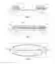
BRIEF DESCRIPTION OF THE DRAWINGS
FIG. 1 is a schematic structural diagram of a sectional-layer shape of an N electrode;
FIG. 2 is a schematic structural diagram of a sectional-layer shape of a P electrode; and
FIG. 3 is a top view of graphical current extension layer (200a) and (200b).
DETAILED DESCRIPTION
As shown in FIGS. 1, 2, and 3: An N-type semiconductor layer 002, a light emitting compound layer 003, and a P-type semiconductor layer 004, and an N-type semiconductor layer 002 that is exposed in the middle of the P-type semiconductor layer 004 after being etched are sequentially disposed on a rectangular substrate 001 having a narrow side L (which is as shown in FIG. 3) less than 300 um. P-type semiconductor layers 004 on two sides of the rectangular substrate 001 are respectively provided with a P pad 101a and an N pad 102a.
P-type semiconductor layers 004 corresponding to the P pad 101a and the N pad 102a are respectively provided with graphical current extension layers 200a and 200b, and the graphical current extension layers 200a and 200b are separately provided with an electrical-insulating layer 201.
The back of the P pad 101a and the back of the N pad 102a are separately provided with a reflector 211.
The P pad 101a is separately electrically connected to two groups of graphical P extended electrodes 101b, and the N pad 102a is electrically connected to an N extended electrode 102b. The N extended electrode 102b is directly disposed on the exposed N-type semiconductor layer 002, and the P extended electrode 101b is disposed on a current extension layer 200.
The P-type semiconductor layer 004 out of disposed areas of the P pad 101a and the N pad 102a is provided with a current barrier layer 300, the current barrier layer 300 is provided with the current extension layer 200, and the two groups of graphical P extended electrodes 101b are disposed on the current extension layer 200.
Graphs of the graphical current extension layer 200b below the N pad 102a and the graphical current extension layer 200a below the P pad 101a may be made by using a photolithographic process.
The reflector 211 may be a conventional medium layer (for example, SiO2/Ti3O5), aluminum layer, or platinum layer.
The electrical-insulating layer 201 is a nitride of aluminum, an oxide of aluminum, an oxide of silicon, or a nitride layer of silicon.
The current extension layers 200a and 200b are current extension layers having a net-dotted surface, and spacing between adjacent net holes is less than 10 um.
It can be seen from FIG. 3 that, for example, circular graphical current extension layers 200a and 200b, which are current extension layers whose surface graph is a net-dotted circular hole, and the diameter of the circular hole is less than 10 um.
Claims
What is claimed is:1. A light emitting diode chip, comprising an N-type semiconductor layer, a light emitting compound layer, and a P-type semiconductor layer sequentially disposed on a rectangular substrate, and an N-type semiconductor layer that is exposed in the middle of the P-type semiconductor layer after being etched, wherein P-type semiconductor layers on two sides of the rectangular substrate are respectively provided with a P pad and an N pad; and a P-type semiconductor layer out of areas of the P pad and the N pad is provided with a current barrier layer, and the current barrier layer is provided with a current extension layer;
P-type semiconductor layers corresponding to the P pad and the N pad are respectively provided with graphical current extension layers, and the graphical current extension layers are respectively provided with electrical-insulating layers; and the back of the P pad and the back of the N pad are respectively provided with reflectors;
the current extension layer is provided with at least two groups of graphical P extended electrodes, and each of the P extended electrodes is electrically connected to the P pad; and
the N pad is electrically connected to the N extended electrode, the N extended electrode is disposed on and is in contact with an exposed N-type semiconductor layer, and the P extended electrode is in contact with the current extension layer.
2. The light emitting diode chip according to claim 1, wherein the graphical current extension layer is a current extension layer whose surface is of a net-dotted circular hole, and the diameter of the circular hole is less than 10 um.
3. The light emitting diode chip according to claim 1, wherein a narrow side of the rectangular substrate is less than 300 um.
4. The light emitting diode chip according to claim 1, wherein the reflector is a medium layer, an aluminum layer, or a platinum layer.
5. The light emitting diode chip according to claim 1, wherein the electrical-insulating layer is a nitride of aluminum, an oxide of aluminum, an oxide of silicon, or a nitride layer of silicon.
Images & Drawings included:

Sources:
- United States Patent and Trademark Office - verify current appl. status at the USPTO↗
Recent applications in this class:
- » 20250072195 2025-02-27
ELECTRONIC DEVICE - » 20250072194 2025-02-27
LIGHT-EMITTING ELEMENT AND METHOD OF PRODUCING LIGHT-EMITTING ELEMENT - » 20250072193 2025-02-27
DISPLAY DEVICE - » 20250072192 2025-02-27
SEMICONDUCTOR DEVICE - » 20250072191 2025-02-27
LED DRIVING DEVICE, METHOD OF FABRICATING LED DRIVING DEVICE AND DISPLAY DEVICE INCLUDING LED DRIVING DEVICE - » 20250072190 2025-02-27
ELECTRONIC DEVICE - » 20250072189 2025-02-27
DISPLAY PANEL - » 20250072188 2025-02-27
DISPLAY DEVICE - » 20250072187 2025-02-27
OPTOELECTRONIC ARRAY AND METHOD FOR MANUFACTURING AN OPTOELECTRONIC ARRAY - » 20250072186 2025-02-27
MULTILAYER STRUCTURE, PACKAGE COMPONENT AND OPTICAL SEMICONDUCTOR DEVICE