High-frequency package
US20170012008A1
2017-01-12
15/119,494
2014-03-11
✅ Patent granted
US 9,685,418 B2
2017-06-20
WO; PCT/JP2014/056370; 20140311
WO; WO2015/136629; 20150917
Michael Trinh
Oblon, McClelland, Maier & Neustadt, L.L.P.
2034-03-11
Abstract:
A high-frequency package has: a resin substrate; a high-frequency device mounted on a side of a first surface of the resin substrate; a ground surface conductor of a ground potential formed on a second surface of the resin substrate on an opposite side to the first surface; a transmission line for a high-frequency signal formed in an inner layer of the resin substrate; and a ground via of a ground potential formed within the resin substrate. A through hole is formed in the ground surface conductor. The ground via is placed between the transmission line and the through hole.
Assignee:
- Mitsubishi Electric Corporation 2,856 🇯🇵 Chiyoda-ku, Japan
Applicant:
Interested in similar patents?
Get notified when new applications in this technology area are published.
Classification:
H01L23/552 » CPC further
Details of semiconductor or other solid state devices Protection against radiation, e.g. light or electromagnetic waves
H01L23/49827 » CPC further
Details of semiconductor or other solid state devices; Arrangements for conducting electric current to or from the solid state body in operation, e.g. leads, terminal arrangements ; Selection of materials therefor consisting of soldered constructions; Leads, on insulating substrates, Via connections through the substrates, e.g. pins going through the substrate, coaxial cables
H01L23/49838 » CPC further
Details of semiconductor or other solid state devices; Arrangements for conducting electric current to or from the solid state body in operation, e.g. leads, terminal arrangements ; Selection of materials therefor consisting of soldered constructions; Leads, on insulating substrates, Geometry or layout
H01L23/498 IPC
Details of semiconductor or other solid state devices; Arrangements for conducting electric current to or from the solid state body in operation, e.g. leads, terminal arrangements ; Selection of materials therefor consisting of soldered constructions Leads, on insulating substrates,
H01L24/16 » CPC further
Arrangements for connecting or disconnecting semiconductor or solid-state bodies; Methods or apparatus related thereto; Means for bonding being attached to, or being formed on, the surface to be connected, e.g. chip-to-package, die-attach, "first-level" interconnects; Manufacturing methods related thereto; Bump connectors ; Manufacturing methods related thereto; Structure, shape, material or disposition of the bump connectors after the connecting process of an individual bump connector
H01L2223/6627 » CPC further
Details relating to semiconductor or other solid state devices covered by the group; Structural electrical arrangements for semiconductor devices not otherwise provided for; Impedance arrangements; High-frequency adaptations; High-frequency electrical connections Waveguides, e.g. microstrip line, strip line, coplanar line
H01L2223/6683 » CPC further
Details relating to semiconductor or other solid state devices covered by the group; Structural electrical arrangements for semiconductor devices not otherwise provided for; Impedance arrangements; High-frequency adaptations for monolithic microwave integrated circuit [MMIC]
H01L23/66 » CPC main
Details of semiconductor or other solid state devices; Structural electrical arrangements for semiconductor devices not otherwise provided for, e.g. in combination with batteries; Impedance arrangements High-frequency adaptations
H01L23/00 IPC
Details of semiconductor or other solid state devices
H01L23/49816 » CPC further
Details of semiconductor or other solid state devices; Arrangements for conducting electric current to or from the solid state body in operation, e.g. leads, terminal arrangements ; Selection of materials therefor consisting of soldered constructions; Leads, on insulating substrates,; Additional leads joined to the metallisation on the insulating substrate, e.g. pins, bumps, wires, flat leads Spherical bumps on the substrate for external connection, e.g. ball grid arrays [BGA]
H01L23/13 » CPC further
Details of semiconductor or other solid state devices; Mountings, e.g. non-detachable insulating substrates characterised by the shape
H01L23/49822 » CPC further
Details of semiconductor or other solid state devices; Arrangements for conducting electric current to or from the solid state body in operation, e.g. leads, terminal arrangements ; Selection of materials therefor consisting of soldered constructions; Leads, on insulating substrates, Multilayer substrates
H01L24/81 » CPC further
Arrangements for connecting or disconnecting semiconductor or solid-state bodies; Methods or apparatus related thereto; Methods for connecting semiconductor or other solid state bodies using means for bonding being attached to, or being formed on, the surface to be connected using a bump connector
H01L2224/81815 » CPC further
Indexing scheme for arrangements for connecting or disconnecting semiconductor or solid-state bodies and methods related thereto as covered by; Methods for connecting semiconductor or other solid state bodies using means for bonding being attached to, or being formed on, the surface to be connected using a bump connector; Bonding techniques; Soldering or alloying Reflow soldering
H01L2924/15151 » CPC further
Indexing scheme for arrangements or methods for connecting or disconnecting semiconductor or solid-state bodies as covered by; Details of package parts other than the semiconductor or other solid state devices to be connected; Die mounting substrate; Shape the die mounting substrate comprising an aperture, e.g. for underfilling, outgassing, window type wire connections
H01L2924/15321 » CPC further
Indexing scheme for arrangements or methods for connecting or disconnecting semiconductor or solid-state bodies as covered by; Details of package parts other than the semiconductor or other solid state devices to be connected; Die mounting substrate; Connection portion the connection portion being formed on the die mounting surface of the substrate being a ball array, e.g. BGA
H05K1/00 » CPC further
Printed circuits
H05K1/00 » CPC further
Printed circuits
H01L2924/1423 » CPC further
Indexing scheme for arrangements or methods for connecting or disconnecting semiconductor or solid-state bodies as covered by; Details of semiconductor or other solid state devices to be connected; Device type; Integrated circuits; Analog devices Monolithic Microwave Integrated Circuit [MMIC]
H01L2924/1579 » CPC further
Indexing scheme for arrangements or methods for connecting or disconnecting semiconductor or solid-state bodies as covered by; Details of package parts other than the semiconductor or other solid state devices to be connected; Die mounting substrate; Material with a principal constituent of the material being a polymer, e.g. polyester, phenolic based polymer, epoxy
Description
FIELD
The present invention relates to a high-frequency package for accommodating a high-frequency device.
BACKGROUND
A high-frequency device that handles a high-frequency signal of a microwave band or a millimeter-wave band has been known. In a high-frequency package that accommodates such a high-frequency device, the high-frequency device is mounted on a dielectric substrate. In some cases, a transmission line for the high-frequency signal is provided in an inner layer of the dielectric substrate (see, for example, Patent Literature 1).
CITATION LIST
Patent Literature
Patent Literature 1: International Publication No. WO2007/091470
SUMMARY
Technical Problem
The inventor of the present application has recognized the following problem for the first time.
Let us consider a case where a “resin substrate” is used as a dielectric substrate on which a high-frequency device is mounted. During the process for manufacturing the resin substrate, moisture originating from cleaning liquid or the like intrudes into a core material or the like. The intruded moisture is confined within the resin substrate due to plating. After that, a reflow process causes gas to be generated within the resin substrate. At this time, if there is no escape for the gas, the gas expands within the resin substrate, which is likely to cause delamination.
In order to avoid such the delamination, it is considered to provide a large number of degassing holes on a ground surface of the resin substrate. In this case, however, a high-frequency signal of a microwave band or a millimeter-wave band originating from a transmission line in an inner layer of the resin substrate is likely to leak to the outside through the degassing holes. This causes deterioration in EMI (Electro-Magnetic Interference) characteristics.
An object of the present invention is to provide a technique that can prevent deterioration in EMI characteristics of a high-frequency package using a resin substrate.
Solution to Problem
In an aspect of the present invention, a high-frequency package has: a resin substrate; a high-frequency device mounted on a side of a first surface of the resin substrate; a ground surface conductor of a ground potential formed on a second surface of the resin substrate on an opposite side to the first surface; a transmission line for a high-frequency signal formed in an inner layer of the resin substrate; and a ground via of a ground potential formed within the resin substrate. A through hole is formed in the ground surface conductor. The ground via is placed between the transmission line and the through hole.
In another aspect of the present invention, a high-frequency package has: a resin substrate; a high-frequency device mounted on a side of a first surface of the resin substrate; a ground surface conductor of a ground potential formed on a second surface of the resin substrate on an opposite side to the first surface; and a transmission line for a high-frequency signal formed in an inner layer of the resin substrate. A through hole is formed in the ground surface conductor. A diameter of the through hole is less than half of a wavelength of the high-frequency signal.
Advantageous Effects of Invention
According to the present invention, it is possible to prevent deterioration in EMI characteristics of a high-frequency package using a resin substrate.
BRIEF DESCRIPTION OF DRAWINGS
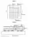
FIG. 1 is a top view of a resin substrate of a high-frequency package according to an embodiment of the present invention.
FIG. 2 is a cross-sectional view of the high-frequency package according to the embodiment of the present invention.
DESCRIPTION OF EMBODIMENTS
A high-frequency package according to an embodiment of the present invention will be described with reference to the accompanying drawings.
Embodiment
FIG. 1 is a top view of a resin substrate of a high-frequency package according to the present embodiment.
FIG. 2 is a cross-sectional view of the high-frequency package according to the present embodiment, and illustrates a cross-sectional structure along a line A-A′ in FIG. 1. It should be noted that in FIG. 1, some components formed in an inner layer of the resin substrate also are illustrated by dashed lines in order to facilitate understanding.
The high-frequency package according to the present embodiment accommodates a high-frequency device 1 that handles a high-frequency signal of a microwave band or a millimeter-wave band. For example, the high-frequency device 1 is exemplified by an MMIC (Monolithic Microwave Integrated Circuit) chip.
In the high-frequency package according to the present embodiment, two substrates facing each other are used. More specifically, as illustrated in FIG. 2, a mother substrate 10 on a lower side and a resin substrate 20 on an upper side are arranged to face each other. Further, inter-substrate connection conductors 15 connecting the mother substrate 10 and the resin substrate 20 are so arranged as to be sandwiched between the mother substrate 10 and the resin substrate 20. The high-frequency device 1 is placed in a space surrounded by the mother substrate 10, the resin substrate 20, and the inter-substrate connection conductors 15. More specifically, the high-frequency device 1 is mounted on the resin substrate 20.
The resin substrate 20 has a first surface 21 and a second surface 22. The first surface 21 is a surface (a device surface) on which side the high-frequency device 1 is mounted and that faces the mother substrate 10. The second substrate 22 is a surface on an opposite side to to the first surface 21, and is used for forming a ground surface as will be described later.
The high-frequency device 1 is mounted on the side of the first surface 21 of the resin substrate 20. More specifically, a surface-layer transmission line 30 and a ground wiring (not illustrated) are formed on the first surface 21 of the resin substrate 20. The high-frequency device 1 is flip-chip connected to the surface-layer transmission line 30 and the ground wire through bumps 31.
On the other hand, a ground surface conductor 40 is formed on the second surface 22 of the resin substrate 20. A potential of the ground surface conductor 40 is a ground potential. By this ground surface conductor 40, a ground surface is formed on the side of the second surface 22 of the resin substrate 20.
In an inner layer of the resin substrate 20, an inner-layer transmission line 50 as a transmission line for the high-frequency signal is formed. The inner-layer transmission line 50 is connected to the above-mentioned surface-layer transmission line 30 through a via 51. For example, the inner-layer transmission line 50 constitutes a tri-plate line. In this case, the above-mentioned ground surface conductor 40 on the second surface 22 also is a constituent element of the tri-plate line.
Furthermore, an inner-layer ground conductor 60 also is formed in an inner layer of the resin substrate 20. A potential of the inner-layer ground conductor 60 is the ground potential.
In the case where the resin substrate 20 is used, a reflow process causes gas to be generated within the resin substrate 20, as described above. At this time, if there is no escape for the gas, the gas expands within the resin substrate 20, which is likely to cause delamination. According to the present embodiment, in order to avoid such the delamination, a large number of through holes 70 for degassing are formed in the ground surface conductor 40 on the second surface 22 (see FIG. 1). However, the high-frequency signal of a microwave band or a millimeter-wave band originating from the inner-layer transmission line 50 is likely to leak to the outside through the through holes 70. This causes deterioration in EMI characteristics.
Therefore, according to the present embodiment, a diameter D of the through hole 70 is designed to be less than half of a wavelength λ of the high-frequency signal (D<λ/2). By decreasing the diameter of the through hole 70 in this manner, a cutoff frequency regarding the through hole 70 becomes equal to or higher than the frequency band used by the high-frequency device 1. As a result, leakage of the high-frequency signal from the through holes 70 is reduced.
Furthermore, according to the present embodiment, a ground via 80 formed within the resin substrate 20 is effectively utilized. A potential of the ground via 80 is the ground potential. For example, the ground via 80 is so formed within the resin substrate 20 as to connect between the ground surface conductor 40 and the inner-layer ground conductor 60. As illustrated in FIGS. 1 and 2, such the ground via 80 is placed between the inner-layer transmission line 50 and the through hole 70. That is, the ground via 80 of the ground potential is placed on the leakage path from the inner-layer transmission line 50 to the through hole 70. As a result of shielding effect by the ground via 80, the leakage of the high-frequency signal from the through hole 70 is reduced.
It is preferable that a large number of ground vias 80 are placed along the inner-layer transmission line 50, as illustrated in FIG. 1. It is further preferable that a large number of ground vias 80 are so placed as to surround the inner-layer transmission line 50. Due to these configurations, the shielding effect by the ground vias 80 becomes prominent, and thus the leakage of the high-frequency signal from the through holes 70 is greatly reduced.
According to the present embodiment, as described above, it is possible to prevent the delamination and to prevent deterioration in the EMI characteristics, even in the case where the resin substrate 20 is used.
The embodiment of the present invention has been described above with reference to the accompanying drawings. Note that the present invention is not limited to the above-described embodiment and can be modified as appropriate by persons skilled in the art without departing from the scope of the invention.
REFERENCE SIGNS LIST
1 high-frequency device, 10 mother substrate, 15 inter-substrate connection conductor, 20 resin substrate, 21 first surface, 22 second surface, 30 surface-layer transmission line, 31 bump, 40 ground surface conductor, 50 inner-layer transmission line, 51 via, 60 inner-layer ground conductor, 70 through hole, 80 ground via.
Claims
1. A high-frequency package comprising:
a resin substrate;
a high-frequency device mounted on a side of a first surface of the resin substrate;
a ground surface conductor of a ground potential formed on a second surface of the resin substrate on an opposite side to the first surface;
a transmission line for a high-frequency signal formed in an inner layer of the resin substrate; and
a ground via of a ground potential formed within the resin substrate, wherein
a through hole is formed in the ground surface conductor, and
the ground via is placed between the transmission line and the through hole.
2. The high-frequency package according to claim 1, wherein
a number of the ground via is plural, and
the plural ground vias are placed along the transmission line.
3. The high-frequency package according to claim 1, wherein a diameter of the through hole is less than half of a wavelength of the high-frequency signal.
4. A high-frequency package comprising:
a resin substrate;
a high-frequency device mounted on a side of a first surface of the resin substrate;
a ground surface conductor of a ground potential formed on a second surface of the resin substrate on an opposite side to the first surface; and
a transmission line for a high-frequency signal formed in an inner layer of the resin substrate, wherein
a through hole is formed in the ground surface conductor, and
a diameter of the through hole is less than half of a wavelength of the high-frequency signal.
Images & Drawings included:

Sources:
- United States Patent and Trademark Office - verify current appl. status at the USPTO↗
Similar patent applications:
- » 20190246495
High-frequency board, high-frequency package, and high-frequency module - » 20200337150
High-frequency board, high-frequency package, and high-frequency module - » 20210368616
High-frequency board, high-frequency package, and high-frequency module - » 20230380052
High-frequency board, high-frequency package, and high-frequency module - » 20140252569
High-frequency semiconductor package and high-frequency semiconductor device - » 20120061133
High-frequency circuit package and high-frequency circuit device - » 20140085858
High-frequency package - » 10781789
High-frequency circuit and high-frequency package - » 20060162157
Economical high-frequency package - » 14882412
High-frequency package
Recent applications in this class:
- » 20250293184 2025-09-18
CASCADED RADIO FREQUENCY SYSTEM IN A SINGLE MULTI-CHIP PACKAGE - » 20250285997 2025-09-11
HETEROGENEOUS INTEGRATION OF RADIO FREQUENCY TRANSISTOR CHIPLETS HAVING INTERCONNECTION TUNING CIRCUITS - » 20250279376 2025-09-04
ELECTRONIC PACKAGE AND MANUFACTURING METHOD THEREOF - » 20250266376 2025-08-21
Semiconductor Component Including One or More Conductors Comprising a Stack of Ferromagnetic and Nonmagnetic Materials - » 20250259948 2025-08-14
PACKAGE COMPRISING DISCRETE ANTENNA DEVICE - » 20250259947 2025-08-14
Semiconductor Device and Method of Forming AIP Package Structure from Separate Assemblies with Bonding Material - » 20250253272 2025-08-07
SIGNAL TRANSMISSION DEVICE - » 20250246560 2025-07-31
RADIO FREQUENCY LEADS HAVING REDUCED LINE WIDTH - » 20250246559 2025-07-31
HIGH FREQUENCY TRANSISTOR - » 20250239542 2025-07-24
SEMICONDUCTOR PACKAGE COMPRISING AN END-FIRE ANTENNA ARRAY
Recent applications for this Assignee:
- » 20250038695 2025-01-30
Electromagnetic interference (EMI) mitigation in pulse width modulation (PWM) inverters using learning-based frequency modulated carriers - » 20240236792 2024-07-11
COMMUNICATION SYSTEM AND COMMUNICATION TERMINAL - » 20240201310 2024-06-20
BASE STATION, TERMINAL DEVICE, POSITIONING METHOD, AND WIRELESS COMMUNICATION SYSTEM - » 20240187960 2024-06-06
COMMUNICATION SYSTEM AND BASE STATION - » 20240137826 2024-04-25
COMMUNICATION SYSTEM AND COMMUNICATION TERMINAL - » 20240129820 2024-04-18
COMMUNICATION SYSTEM AND BASE STATION - » 20240032137 2024-01-25
USER APPARATUS, BASE STATION AND COMMUNICATION SYSTEM - » 20240008120 2024-01-04
COMMUNICATION SYSTEM, BASE STATION AND USER EQUIPMENT - » 20240007923 2024-01-04
COMMUNICATION SYSTEM AND COMMUNICATION TERMINAL - » 20230422201 2023-12-28
COMMUNICATION TERMINAL AND COMMUNICATION SYSTEM