Pixel cell circuits of compensation feedback voltage
US20170018246A1
2017-01-19
14/778,088
2015-08-21
✅ Patent granted
US 9,570,034 B2
2017-02-14
WO; PCT/CN2015/087722; 20150821
-
Jennifer Nguyen
Leong C. Lei
2035-08-21
Abstract:
The present disclosure relates to a pixel cell circuit of compensation feedback voltage. The pixel cell circuit is provided with the compensation capacitance (C_co), one end of the compensation capacitance (C_co) electrically connects to the compensation level wirings G(m)_co, and the other end of the compensation capacitance (C_co) electrically connects to the drain of the TFT (T1) and the pixel electrode (P). A level of the compensation signals transmitted by the compensation level wirings G(m)_co is opposite to the level of the scanning signals transmitted by the scanning lines G(m). When the pixel electrode has been fully charged, the compensation capacitance generates a pull-up feedback voltage for compensating the pull-down voltage caused by the parasitic capacitance so as to eliminate the effects toward the pixel electrodes caused by the scanning signals transmitted by the scanning lines. This configuration not only decreases the flickers, but also the image sticking. In brief, the display uniformity and the display performance are enhanced.
Assignee:
- SHENZHEN CHINA STAR OPTOELECTRONICS TECHNOLOGY CO, LTD. 11 🇨🇳 Shenzhen, Guandong, China
Applicant:
Interested in similar patents?
Get notified when new applications in this technology area are published.
Classification:
G02F1/13439 » CPC further
Devices or arrangements for the control of the intensity, colour, phase, polarisation or direction of light arriving from an independent light source, e.g. switching, gating or modulating; Non-linear optics for the control of the intensity, phase, polarisation or colour based on liquid crystals, e.g. single liquid crystal display cells; Constructional arrangements; Operation of liquid crystal cells; Circuit arrangements; Constructional arrangements; Manufacturing methods; Electrodes characterised by their electrical, optical, physical properties; materials therefor; method of making
G09G3/3677 » CPC further
Control arrangements or circuits, of interest only in connection with visual indicators other than cathode-ray tubes for presentation of an assembly of a number of characters, e.g. a page, by composing the assembly by combination of individual elements arranged in a matrix no fixed position being assigned to or needed to be assigned to the individual characters or partial characters by control of light from an independent source using liquid crystals; Control of matrices with row and column drivers; Details of drivers for scan electrodes suitable for active matrices only
G09G3/3688 » CPC further
Control arrangements or circuits, of interest only in connection with visual indicators other than cathode-ray tubes for presentation of an assembly of a number of characters, e.g. a page, by composing the assembly by combination of individual elements arranged in a matrix no fixed position being assigned to or needed to be assigned to the individual characters or partial characters by control of light from an independent source using liquid crystals; Control of matrices with row and column drivers; Details of drivers for data electrodes suitable for active matrices only
H01L27/124 » CPC further
Devices consisting of a plurality of semiconductor or other solid-state components formed in or on a common substrate including semiconductor components specially adapted for rectifying, oscillating, amplifying or switching and having at least one potential-jump barrier or surface barrier; including integrated passive circuit elements with at least one potential-jump barrier or surface barrier the substrate being other than a semiconductor body, e.g. an insulating body comprising a plurality of TFTs formed on a non-semiconducting substrate, e.g. driving circuits for AMLCDs with a particular composition, shape or layout of the wiring layers specially adapted to the circuit arrangement, e.g. scanning lines in LCD pixel circuits
G02F2201/123 » CPC further
Constructional arrangements not provided for in groups - electrode pixel
H01L27/12 IPC
Devices consisting of a plurality of semiconductor or other solid-state components formed in or on a common substrate including semiconductor components specially adapted for rectifying, oscillating, amplifying or switching and having at least one potential-jump barrier or surface barrier; including integrated passive circuit elements with at least one potential-jump barrier or surface barrier the substrate being other than a semiconductor body, e.g. an insulating body
G09G2300/0426 » CPC further
Aspects of the constitution of display devices; Structural and physical details of display devices; Structural details of the set of electrodes Layout of electrodes and connections
G09G2300/0819 » CPC further
Aspects of the constitution of display devices; Active matrix structure, i.e. with use of active elements, inclusive of non-linear two terminal elements, in the pixels together with light emitting or modulating elements; Several active elements per pixel in active matrix panels used for counteracting undesired variations, e.g. feedback or autozeroing
G09G2320/0247 » CPC further
Control of display operating conditions; Improving the quality of display appearance Flicker reduction other than flicker reduction circuits used for single beam cathode-ray tubes
G09G3/36 IPC
Control arrangements or circuits, of interest only in connection with visual indicators other than cathode-ray tubes for presentation of an assembly of a number of characters, e.g. a page, by composing the assembly by combination of individual elements arranged in a matrix no fixed position being assigned to or needed to be assigned to the individual characters or partial characters by control of light from an independent source using liquid crystals
G02F1/1343 IPC
Devices or arrangements for the control of the intensity, colour, phase, polarisation or direction of light arriving from an independent light source, e.g. switching, gating or modulating; Non-linear optics for the control of the intensity, phase, polarisation or colour based on liquid crystals, e.g. single liquid crystal display cells; Constructional arrangements; Operation of liquid crystal cells; Circuit arrangements; Constructional arrangements; Manufacturing methods Electrodes
G02F1/1362 IPC
Devices or arrangements for the control of the intensity, colour, phase, polarisation or direction of light arriving from an independent light source, e.g. switching, gating or modulating; Non-linear optics for the control of the intensity, phase, polarisation or colour based on liquid crystals, e.g. single liquid crystal display cells; Constructional arrangements; Operation of liquid crystal cells; Circuit arrangements; Liquid crystal cells structurally associated with a semi-conducting layer or substrate, e.g. cells forming part of an integrated circuit Active matrix addressed cells
G09G3/3696 » CPC main
Control arrangements or circuits, of interest only in connection with visual indicators other than cathode-ray tubes for presentation of an assembly of a number of characters, e.g. a page, by composing the assembly by combination of individual elements arranged in a matrix no fixed position being assigned to or needed to be assigned to the individual characters or partial characters by control of light from an independent source using liquid crystals; Control of matrices with row and column drivers Generation of voltages supplied to electrode drivers
G02F1/136286 » CPC further
Devices or arrangements for the control of the intensity, colour, phase, polarisation or direction of light arriving from an independent light source, e.g. switching, gating or modulating; Non-linear optics for the control of the intensity, phase, polarisation or colour based on liquid crystals, e.g. single liquid crystal display cells; Constructional arrangements; Operation of liquid crystal cells; Circuit arrangements; Liquid crystal cells structurally associated with a semi-conducting layer or substrate, e.g. cells forming part of an integrated circuit; Active matrix addressed cells Wiring, e.g. gate line, drain line
G02F1/1368 » CPC further
Devices or arrangements for the control of the intensity, colour, phase, polarisation or direction of light arriving from an independent light source, e.g. switching, gating or modulating; Non-linear optics for the control of the intensity, phase, polarisation or colour based on liquid crystals, e.g. single liquid crystal display cells; Constructional arrangements; Operation of liquid crystal cells; Circuit arrangements; Liquid crystal cells structurally associated with a semi-conducting layer or substrate, e.g. cells forming part of an integrated circuit; Active matrix addressed cells in which the switching element is a three-electrode device
Description
BACKGROUND OF THE INVENTION
1. Field of the Invention
The present disclosure relates to liquid crystal display technology, and more particularly to a pixel cell circuit of compensation feedback voltage.
2. Discussion of the Related Art
LCDs typically are characterized by attributes including thin, power-saving, and low radiation, and thus have been widely adopted by electronic devices, such as liquid crystal televisions, mobile phones, personal digital assistant (PDA), digital cameras, and monitors for computers and notebooks. The LCD is dominant in the flat display field.
Currently, LCDs are mainly backlight type, which may include a housing, a liquid crystal panel and a backlight module arranged within the housing. The liquid crystal panel is the key component of the LCD. However, the liquid crystal panel needs the light source provided by the backlight module to display images.
The liquid crystal panel usually includes a color filter (CF), a Thin Film Transistor Array Substrate (TFT Array Substrate), and a liquid Crystal Layer between the two substrates. Pixel electrodes and common electrodes are arranged at internal surfaces of the two substrates facing toward each other. The alignment of the liquid crystal molecules may be changed by applying the voltage to the liquid crystal molecules such that the light beams from the backlight module are reflected to generate the images. The array substrate may include a plurality of pixels arranged in a matrix. Each of the pixels includes Thin Film Transistor (TFT) to control the voltage of the pixel electrode so as to change the rotating angle of the liquid crystal. As such, the density of the optical field may be controlled.
There are a variety of structures of the TFTs. Currently, most of the LCDs adopt bottom-gate structure. The gate and the source/drain are overlapped in the bottom of the TFT, and parasitic capacitance (Cgs) may be generated in the overlapped area.
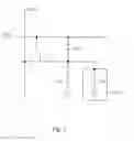
FIG. 1 is a circuit diagram of the conventional pixel cell circuit. The pixel cell circuit includes the TFT (T1). The gate of the TFT (T1) electrically connects with the scanning line G(m) corresponding to row of the pixel cell, the source of the TFT (T1) electrically connects with the data line D(n) corresponding to the column of the pixel cell, and the drain electrically connects with the pixel electrode (P). Two ends of the parasitic capacitance (Cgs) electrically connects with the gate and the drain of the TFT (T1). One end of a storage capacitance (Cst) electrically connects with the drain of the TFT (T1), and the other end of the storage capacitance (Cst) connects with a constant voltage. One end of the liquid crystal capacitor (Clc) electrically connect to the drain of the TFT (T1), and the other end of the liquid crystal capacitor (Clc) connects with the constant voltage.
The voltage of the pixel electrode (P) may be interfered by the level of the gate of the TFT (T1) due to the parasitic capacitance (Cgs). Also referring to FIG. 2, when the pixel electrode (P) has been charged fully, the level of the gate of the TFT (T1) is pulled down instantly. The voltage of the pixel electrode (P) may also be pulled down due to the capacitance coupling effect. As such, one feedthrough voltage (Vft_1) is generated, and the magnitude of the feedthrough voltage (Vft1) may be represented by the equation below:
Vft1=(Vgh−Vgl)×Cgs/Ctotal
Wherein Vgh represents the high level of the scanning signals transmitted by the scanning line G(m), Vgl represents the low level of the scanning signals transmitted by the scanning line G(m), Ctotal represents a sum of the capacitance connected by the pixel electrode (P), including the liquid crystal capacitor (Clc), the storage capacitance (Cst), and the parasitic capacitance (Cgs).
The voltage of the positive and negative frames of the pixel electrode (P) may be affected by the parasitic capacitance (Cgs), which results in asymmetric voltage of the positive and negative frames. This may cause problems such as flicker and image sticking, and thus the display performance may be affected. In addition, the RC delay with respect to different areas of the panel may also cause the difference of the feedback voltage. This may result in non-uniform voltage of the common electrode (Vcom), and may cause serious flicker.
SUMMARY
The object of the invention is to provide a pixel cell circuit of compensation feedback voltage for compensating the feedback voltage resulting from the parasitic capacitance. This configuration not only decreases the flickers, but also the image sticking. In brief, the display uniformity and the display performance are enhanced.
In one aspect, a pixel cell circuit of the compensation feedback voltage includes: a TFT, a gate of the TFT electrically connecting to a scanning line corresponding to a row of the pixel cell, a source of the TFT electrically connecting to a data line corresponding to a column of the pixel cell, and a drain of the TFT electrically connecting to a pixel electrode; the pixel electrode electrically connecting to the drain of the TFT; a parasitic capacitance, one end of the parasitic capacitance electrically connecting to the gate of the TFT, and the other end of the parasitic capacitance electrically connecting to the drain of the TFT and the pixel electrode; a compensation capacitance, one end of the compensation capacitance electrically connecting to the compensation level wirings, and the other end of the compensation capacitance electrically connecting to the drain of the TFT and the pixel electrode; and compensation level wirings, a level of the compensation signals transmitted by the compensation level wirings being opposite to the level of the scanning signals transmitted by the scanning lines.
Wherein the pixel cell circuit further includes an inverter, an input end of the inverter electrically connects to the scanning line, and the output end of the inverter electrically connects to the compensation level wirings.
Wherein the pixel cell circuit further includes a storage capacitance and a liquid crystal capacitor, one end of the storage capacitance electrically connects to the drain of the TFT, and the other end of the storage capacitance connects to a constant voltage, and one end of the liquid crystal capacitor electrically connects to the drain of the TFT, and the other end of the liquid crystal capacitor electrically connects to the constant voltage.
Wherein the compensation level wirings, the gate of the TFT, and the scanning line are on the same layer, and the compensation capacitance is constituted by compensation level wirings and a drain of the TFT.
Wherein the compensation level wirings, the gate of the TFT, and the scanning line are on the same layer, and the compensation capacitance is constituted by compensation level wirings and a drain of the TFT.
Wherein the pixel electrode is ITO electrode.
Wherein C_co×V_co=(Vgh−Vgl)×Cgs;
wherein C_co represents a compensation capacitance, V_co represents a voltage difference between the high and low level of the compensation signals transmitted by the compensation level wirings, Vgh represents the high level of the scanning signals transmitted by the signal line, Vgl represents the low level of the scanning signals transmitted by the signal lines, and Cgs represents parasitic capacitance.
Wherein:
V_co=Vgh−Vgl; and C_co=Cgs.
Wherein:
V_co<Vgh−Vgl; and C_co>Cgs.
In another aspect, a pixel cell circuit of the compensation feedback voltage includes: a TFT, a gate of the TFT electrically connecting to a scanning line corresponding to a row of the pixel cell, a source of the TFT electrically connecting to a data line corresponding to a column of the pixel cell, and a drain of the TFT electrically connecting to a pixel electrode; the pixel electrode electrically connecting to the drain of the TFT; a parasitic capacitance, one end of the parasitic capacitance electrically connecting to the gate of the TFT, and the other end of the parasitic capacitance electrically connecting to the drain of the TFT and the pixel electrode; a compensation capacitance, one end of the compensation capacitance electrically connecting to the compensation level wirings, and the other end of the compensation capacitance electrically connecting to the drain of the TFT and the pixel electrode; compensation level wirings, a level of the compensation signals transmitted by the compensation level wirings being opposite to the level of the scanning signals transmitted by the scanning lines; an inverter, an input end of the inverter electrically connecting to the scanning line, and the output end of the inverter electrically connecting to the compensation level wirings; a storage capacitance and a liquid crystal capacitor, one end of the storage capacitance electrically connecting to the drain of the TFT, and the other end of the storage capacitance connecting to a constant voltage, and one end of the liquid crystal capacitor electrically connecting to the drain of the TFT, and the other end of the liquid crystal capacitor electrically connecting to the constant voltage;
C_co×V_co=(Vgh−Vgl)×Cgs; and wherein C_co represents a compensation capacitance, V_co represents a voltage difference between the high and low level of the compensation signals transmitted by the compensation level wirings, Vgh represents the high level of the scanning signals transmitted by the signal line, Vgl represents the low level of the scanning signals transmitted by the signal lines, and Cgs represents parasitic capacitance.
In view of the above, the pixel cell circuit of compensation feedback voltage is configured with the compensation capacitance. One end of the compensation capacitance electrically connects with the wiring of the compensation level, and the other end of the compensation capacitance electrically connects with the pixel electrode. The level of the compensation signals transmitted by the compensation level wiring is opposite to the level of the scanning signals transmitted by the signal lines. When the pixel electrode has been fully charged, the compensation capacitance generates a pull-up feedback voltage for compensating the pull-down voltage caused by the parasitic capacitance so as to eliminate the effects toward the pixel electrodes caused by the scanning signals transmitted by the scanning lines. This configuration not only decreases the flickers, but also the image sticking. In brief, the display uniformity and the display performance are enhanced.
In order to further understand the characteristics of the invention as well as technical content, see the following detailed description of the present invention and the accompanying drawings, drawings, however, for reference purposes only and description of use is not intended to limit the present invention.
BRIEF DESCRIPTION OF THE DRAWINGS
Below in conjunction with the accompanying drawings, through a specific embodiment of the present invention is described in detail, and will make apparent the technical solution of the present invention, and other beneficial effects.
FIG. 1 is a circuit diagram of the conventional pixel cell circuit.
FIG. 2 is a sectional view showing the voltage waveform of the pixel electrode within the conventional pixel cell circuit.
FIG. 3 is a circuit diagram of the pixel cell circuit of the compensation feedback voltage in accordance with one embodiment.
FIG. 4 is a sectional view of the compensation capacitance within the pixel cell circuit of the compensation feedback voltage in accordance with one embodiment.
FIG. 5 is a waveform diagram of the compensation signals transmitted by the compensation level wirings and the scanning signals transmitted by the signal lines of the pixel cell circuit of the compensation feedback voltage in accordance with one embodiment.
FIG. 6 is a sectional view of the voltage waveform of the pixel electrode of the pixel cell circuit of the compensation feedback voltage in accordance with one embodiment.
DETAILED DESCRIPTION OF THE EMBODIMENTS
Embodiments of the invention will now be described more fully hereinafter with reference to the accompanying drawings, in which embodiments of the invention are shown.
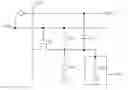
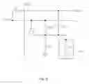
FIG. 3 is a circuit diagram of the pixel cell circuit of the compensation feedback voltage in accordance with one embodiment. The pixel cell circuit includes a TFT (T1), a pixel electrode (P), a parasitic capacitance (Cgs), a compensation capacitance (C_co), and compensation level wirings G(m)_co.
A gate of the TFT (T1) electrically connects to the scanning line G(m) corresponding to a row of the pixel cell, a source of the TFT (T1) electrically connects to the data line D(n) corresponding to a column of the pixel cell, and a drain of the TFT (T1) electrically connects to the pixel electrode (P).
The pixel electrode (P) electrically connects to the drain of the TFT (T1).
One end of the parasitic capacitance (Cgs) electrically connects to the gate of the TFT (T1), and the other end of the parasitic capacitance (Cgs) electrically connects to the drain of the TFT (T1) and the pixel electrode (P).
One end of the compensation capacitance (C_co) electrically connects to the compensation level wirings G(m)_co, and the other end of the compensation capacitance (C_co) electrically connects to the drain of the TFT (T1) and the pixel electrode (P).
In addition, the level of the compensation level wirings G(m)_co and the level of the compensation signals transmitted by the compensation level wirings G(m)_co are opposite to the level of the scanning signals transmitted by the scanning lines G(m).
In addition, an inverter (F) is configured such that the level of the compensation signals transmitted by the compensation level wirings G(m)_co is opposite to that of the scanning signals transmitted by the scanning line G(m). The input end of the inverter (F) electrically connects to the scanning line G(m), and the output end of the inverter (F) electrically connects to the compensation level wirings G(m)_co. As shown in FIG. 5, when the scanning signals transmitted by the scanning line G(m) is at high level (Vgh), after being inverted by the inverter (F), the compensation signals transmitted by the compensation level wirings G(m)_co is at low level (Vgl). Correspondingly, when the scanning signals transmitted by the scanning line G(m) is at low level (Vgl), after being inverted by the inverter (F), the compensation signals transmitted by the compensation level wirings G(m)_co is at high level (Vgh).
In the embodiment, the pixel cell circuit of the compensation feedback voltage also includes a storage capacitance (Cst) and a liquid crystal capacitor (Clc). One end of the storage capacitance (Cst) electrically connects to the drain of the TFT (T1), and the other end of the storage capacitance (Cst) connects to a constant voltage. One end of the liquid crystal capacitor (Clc) electrically connects to the drain of the TFT (T1), and the other end of the liquid crystal capacitor (Clc) electrically connects to the constant voltage.
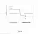
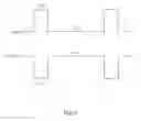
In the embodiment, the compensation level wirings G(m)_co, the gate of the TFT (T1), and the scanning line G(m) are on the same layer. That is, the above are covered by the gate insulation layer. With respect to the manufacturing process, the compensation level wirings G(m)_co, the gate of the TFT (T1), and the scanning line G(m) are manufactured by patterning the first metallic layer. The source and the drain of the TFT (T1) are manufactured by patterning the second metallic layer. The pixel electrode (P) is the ITO electrode.
As shown in FIG. 4, the compensation capacitance (C_co) may be constituted by compensation level wirings G(m)_co and the drain 4 of the TFT (T1). A gate insulation layer 2 and a source layer 3 are provided between the compensation level wirings G(m)_co and the TFT (T1).
The compensation capacitance (C_co) may be constituted by the compensation level wirings G(m)_co and the pixel electrode (P).
Referring to FIGS. 2, 5 and 6, after the pixel electrode (P) is fully charged, the scanning signals transmitted by the scanning line G(m) transits from the high level (Vgh) to the low level (Vgl). The gate level of the TFT (T1) is pulled down. The voltage of the pixel electrode (P) is also pulled down due to the parasitic capacitance (Cgs) so as to generate a pull-down feedback voltage (Vft1). At the same time, due to the operations of the inverter (F), the level of the compensation signals transmitted by the compensation level wirings G(m)_co transits from the low level (Vgl) to the high level (Vgh). The voltage of the pixel electrode (P) generates a pull-up feedback voltage (Vft2) as being affected by the compensation capacitance (C_co). The magnitude of the pull-up feedback voltage (Vft2) equals to the pull-down feedback voltage (Vft1) such that the voltage of the pixel electrode (P) remains the same. That is, the pull-up feedback voltage (Vft2) generated by the compensation capacitance (C_co) compensates the pull-down feedback voltage (Vft1) caused by the parasitic capacitance (Cgs), which prevents the pixel electrode (P) from being affected by the scanning signals transmitted by the scanning line G(m). This configuration not only decreases the flickers, but also the image sticking. In brief, the display uniformity and the display performance are enhanced
Further, the magnitude of the compensation capacitance (C_co) may be configured to be the same with the parasitic capacitance (Cgs). At the same time, the voltage difference (V_Co) between the high and low level of the compensation signals transmitted by the compensation level wirings G(m)_co equals to the voltage difference between the high level (Vgh) and the low level (Vgl) of the scanning signals transmitted by the scanning line G(m). That is:
V_co=Vgh−Vgl; and
C_co=Cgs;
In order to decrease the loading of the scanning line G(m), the voltage difference (V_Co) between the high and low level of the compensation signals transmitted by the compensation level wirings G(m)_co may be configured to be smaller than the voltage difference between the high level (Vgh) and the low level (Vgl) of the scanning signals transmitted by the scanning line G(m), which may be accomplished by increasing the compensation capacitance (C_co).
V_co<Vgh−Vgl;
C_co>Cgs;
As long as the equation below is guaranteed.
C_co×V_co=(Vgh−Vgl)×Cgs
In view of the above, the pixel cell circuit of compensation feedback voltage is configured with the compensation capacitance. One end of the compensation capacitance electrically connects with the wiring of the compensation level, and the other end of the compensation capacitance electrically connects with the pixel electrode. The level of the compensation signals transmitted by the compensation level wiring is opposite to the level of the scanning signals transmitted by the signal lines. When the pixel electrode has been fully charged, the compensation capacitance generates a pull-up feedback voltage for compensating the pull-down voltage caused by the parasitic capacitance so as to eliminate the effects toward the pixel electrodes caused by the scanning signals transmitted by the scanning lines. This configuration not only decreases the flickers, but also the image sticking. In brief, the display uniformity and the display performance are enhanced.
It is believed that the present embodiments and their advantages will be understood from the foregoing description, and it will be apparent that various changes may be made thereto without departing from the spirit and scope of the invention or sacrificing all of its material advantages, the examples hereinbefore described merely being preferred or exemplary embodiments of the invention.
Claims
What is claimed is:1. A pixel cell circuit of the compensation feedback voltage, comprising:
a TFT, a gate of the TFT electrically connecting to a scanning line corresponding to a row of the pixel cell, a source of the TFT electrically connecting to a data line corresponding to a column of the pixel cell, and a drain of the TFT electrically connecting to a pixel electrode;
the pixel electrode electrically connecting to the drain of the TFT;
a parasitic capacitance, one end of the parasitic capacitance electrically connecting to the gate of the TFT, and the other end of the parasitic capacitance electrically connecting to the drain of the TFT and the pixel electrode;
a compensation capacitance, one end of the compensation capacitance electrically connecting to the compensation level wirings, and the other end of the compensation capacitance electrically connecting to the drain of the TFT and the pixel electrode; and
compensation level wirings, a level of the compensation signals transmitted by the compensation level wirings being opposite to the level of the scanning signals transmitted by the scanning lines.
2. The pixel cell circuit of the compensation feedback voltage as claimed in claim 1, wherein the pixel cell circuit further comprises an inverter, an input end of the inverter electrically connects to the scanning line, and the output end of the inverter electrically connects to the compensation level wirings.
3. The pixel cell circuit of the compensation feedback voltage as claimed in claim 1, wherein the pixel cell circuit further comprises a storage capacitance and a liquid crystal capacitor, one end of the storage capacitance electrically connects to the drain of the TFT, and the other end of the storage capacitance connects to a constant voltage, and one end of the liquid crystal capacitor electrically connects to the drain of the TFT, and the other end of the liquid crystal capacitor electrically connects to the constant voltage.
4. The pixel cell circuit of the compensation feedback voltage as claimed in claim 2, wherein the compensation level wirings, the gate of the TFT, and the scanning line are on the same layer, and the compensation capacitance is constituted by compensation level wirings and a drain of the TFT.
5. The pixel cell circuit of the compensation feedback voltage as claimed in claim 1, wherein the compensation level wirings, the gate of the TFT, and the scanning line are on the same layer, and the compensation capacitance is constituted by compensation level wirings and a drain of the TFT.
6. The pixel cell circuit of the compensation feedback voltage as claimed in claim 5, wherein the pixel electrode is ITO electrode.
7. The pixel cell circuit of the compensation feedback voltage as claimed in claim 1, wherein
C_co×V_co=(Vgh−Vgl)×Cgs
wherein C_co represents a compensation capacitance, V_co represents a voltage difference between the high and low level of the compensation signals transmitted by the compensation level wirings, Vgh represents the high level of the scanning signals transmitted by the signal line, Vgl represents the low level of the scanning signals transmitted by the signal lines, and Cgs represents parasitic capacitance.
8. The pixel cell circuit of the compensation feedback voltage as claimed in claim 7, wherein:
V_co=Vgh−Vgl; and
C_co=Cgs;
9. The pixel cell circuit of the compensation feedback voltage as claimed in claim 7, wherein:
V_co<Vgh−Vgl; and
C_co>Cgs;
10. A pixel cell circuit of the compensation feedback voltage, comprising:
a TFT, a gate of the TFT electrically connecting to a scanning line corresponding to a row of the pixel cell, a source of the TFT electrically connecting to a data line corresponding to a column of the pixel cell, and a drain of the TFT electrically connecting to a pixel electrode;
the pixel electrode electrically connecting to the drain of the TFT;
a parasitic capacitance, one end of the parasitic capacitance electrically connecting to the gate of the TFT, and the other end of the parasitic capacitance electrically connecting to the drain of the TFT and the pixel electrode;
a compensation capacitance, one end of the compensation capacitance electrically connecting to the compensation level wirings, and the other end of the compensation capacitance electrically connecting to the drain of the TFT and the pixel electrode;
compensation level wirings, a level of the compensation signals transmitted by the compensation level wirings being opposite to the level of the scanning signals transmitted by the scanning lines;
an inverter, an input end of the inverter electrically connecting to the scanning line, and the output end of the inverter electrically connecting to the compensation level wirings;
a storage capacitance and a liquid crystal capacitor, one end of the storage capacitance electrically connecting to the drain of the TFT, and the other end of the storage capacitance connecting to a constant voltage, and one end of the liquid crystal capacitor electrically connecting to the drain of the TFT, and the other end of the liquid crystal capacitor electrically connecting to the constant voltage;
C_co×V_co=(Vgh−Vgl)×Cgs; and
wherein C_co represents a compensation capacitance, V_co represents a voltage difference between the high and low level of the compensation signals transmitted by the compensation level wirings, Vgh represents the high level of the scanning signals transmitted by the signal line, Vgl represents the low level of the scanning signals transmitted by the signal lines, and Cgs represents parasitic capacitance.
11. The pixel cell circuit of the compensation feedback voltage as claimed in claim 10, wherein the compensation level wirings, the gate of the TFT, and the scanning line are on the same layer, and the compensation capacitance is constituted by compensation level wirings and a drain of the TFT.
12. The pixel cell circuit of the compensation feedback voltage as claimed in claim 10, wherein the compensation level wirings, the gate of the TFT, and the scanning line are on the same layer, and the compensation capacitance is constituted by compensation level wirings and at least one pixel electrode.
13. The pixel cell circuit of the compensation feedback voltage as claimed in claim 12, wherein the pixel electrode is ITO electrode.
14. The pixel cell circuit of the compensation feedback voltage as claimed in claim 10, wherein:
V_co=Vgh−Vgl; and
C_co=Cgs.
15. The pixel cell circuit of the compensation feedback voltage as claimed in claim 10, wherein:
V_co<Vgh−Vgl; and
C_co>Cgs;
Images & Drawings included:

Sources:
- United States Patent and Trademark Office - verify current appl. status at the USPTO↗
Recent applications in this class:
- » 20250232741 2025-07-17
PULSE WIDTH MODULATION FOR PHASE-MODULATING DISPLAY - » 20250225949 2025-07-10
CHOLESTEROL LIQUID CRYSTAL DISPLAY AND DRIVING METHOD THEREOF - » 20250210007 2025-06-26
ELECTRO-OPTICAL DEVICE AND DISPLAY DEVICE - » 20250191550 2025-06-12
POWER MANAGEMENT DEVICE - » 20250182714 2025-06-05
DUAL-VOLTAGE PIXEL CIRCUITRY FOR LIQUID CRYSTAL DISPLAY - » 20250166583 2025-05-22
ARRAY SUBSTRATE, DISPLAY APPARATUS AND CONTROL METHOD THEREOF - » 20250124891 2025-04-17
COMPENSATION CIRCUIT AND DISPLAY DEVICE - » 20250095604 2025-03-20
DIMMING DEVICE ANGULAR UNIFORMITY CORRECTION - » 20250095603 2025-03-20
PIXEL DRIVING METHOD, PIXEL DRIVING CIRCUIT AND DISPLAY DEVICE - » 20250078775 2025-03-06
DISPLAY PANEL, DRIVING METHOD THEREOF, AND ELECTRONIC DEVICE THEREOF
Recent applications for this Assignee:
- » 20190086746 2019-03-21
Array substrate and display panel - » 20180342541 2018-11-29
TFT substrate manufacturing method - » 20180268769 2018-09-20
Driving method for display panel, timing controller and liquid crystal display - » 20180259800 2018-09-13
Liquid crystal display panel and liquid crystal display - » 20170155082 2017-06-01
Encapsulating structure of flexible OLED device and flexible display device - » 20160286207 2016-09-29
3D shutter glasses and 3D display system - » 20140312341 2014-10-23
Transistor, the Preparation Method Therefore, and Display Panel - » 20140218002 2014-08-07
Power system and control method thereof - » 20140184979 2014-07-03
Slim bezel liquid crystal display device - » 20130094241 2013-04-18
LED back light module and liquid crystal display device