Method of manufacturing semiconductor device including forming protective film within recess in substrate
US20170040171A1
2017-02-09
15/304,558
2014-07-31
✅ Patent granted
US 9,947,544 B2
2018-04-17
WO; PCT/JP2014/070246; 20140731
WO; WO2016/017007; 20160204
Jay C Chang
Studebaker & Brackett PC
2034-07-31
Abstract:
An n-type layer (3) is formed by implanting an n-type impurity in a back surface of a Si substrate (1). A recess (4) is formed in the back surface of the Si substrate (1). After forming the n-type layer (3), an oxide film (5) is formed on the back surface and in the recess (4). The oxide film (5) on the back surface is removed while the oxide film (5) in the recess (4) is left. After removing the oxide film (5), an Al—Si film (6) is formed on the back surface, A metal electrode (7) is formed on the Al—Si film (6). The oxide film (5) in the recess (4) prevents Al from diffusing from the Al—Si film (6) into the Si substrate (1) through the recess (4).
Assignee:
- MITSUBISHI ELECTRIC CORPORATION 16,560 🇯🇵 TOKYO, Japan
Applicant:
Interested in similar patents?
Get notified when new applications in this technology area are published.
Classification:
H01L21/324 » CPC further
Processes or apparatus adapted for the manufacture or treatment of semiconductor or solid state devices or of parts thereof; Manufacture or treatment of semiconductor devices or of parts thereof the devices having at least one potential-jump barrier or surface barrier, e.g. PN junction, depletion layer or carrier concentration layer the devices having semiconductor bodies comprising elements of Group IV of the Periodic System or AB compounds with or without impurities, e.g. doping materials; Treatment of semiconductor bodies using processes or apparatus not provided for in groups - Thermal treatment for modifying the properties of semiconductor bodies, e.g. annealing, sintering
H01L21/265 IPC
Processes or apparatus adapted for the manufacture or treatment of semiconductor or solid state devices or of parts thereof; Manufacture or treatment of semiconductor devices or of parts thereof the devices having at least one potential-jump barrier or surface barrier, e.g. PN junction, depletion layer or carrier concentration layer the devices having semiconductor bodies comprising elements of Group IV of the Periodic System or AB compounds with or without impurities, e.g. doping materials; Bombardment with radiation with high-energy radiation producing ion implantation
H01L21/283 » CPC main
Processes or apparatus adapted for the manufacture or treatment of semiconductor or solid state devices or of parts thereof; Manufacture or treatment of semiconductor devices or of parts thereof the devices having at least one potential-jump barrier or surface barrier, e.g. PN junction, depletion layer or carrier concentration layer the devices having semiconductor bodies comprising elements of Group IV of the Periodic System or AB compounds with or without impurities, e.g. doping materials; Manufacture of electrodes on semiconductor bodies using processes or apparatus not provided for in groups - Deposition of conductive or insulating materials for electrodes conducting electric current
H01L29/456 » CPC further
Semiconductor devices adapted for rectifying, amplifying, oscillating or switching, or capacitors or resistors with at least one potential-jump barrier or surface barrier, e.g. PN junction depletion layer or carrier concentration layer; Details of semiconductor bodies or of electrodes thereof; Multistep manufacturing processes therefor; Electrodes ; Multistep manufacturing processes therefor characterised by the materials of which they are formed; Ohmic electrodes on silicon
H01L21/76841 » CPC further
Processes or apparatus adapted for the manufacture or treatment of semiconductor or solid state devices or of parts thereof; Manufacture or treatment of devices consisting of a plurality of solid state components formed in or on a common substrate or of parts thereof; Manufacture of integrated circuit devices or of parts thereof; Manufacture of specific parts of devices defined in group; Applying interconnections to be used for carrying current between separate components within a device comprising conductors and dielectrics characterised by the formation and the after-treatment of the conductors Barrier, adhesion or liner layers
H01L29/45 IPC
Semiconductor devices adapted for rectifying, amplifying, oscillating or switching, or capacitors or resistors with at least one potential-jump barrier or surface barrier, e.g. PN junction depletion layer or carrier concentration layer; Details of semiconductor bodies or of electrodes thereof; Multistep manufacturing processes therefor; Electrodes ; Multistep manufacturing processes therefor characterised by the materials of which they are formed Ohmic electrodes
H01L21/285 IPC
Processes or apparatus adapted for the manufacture or treatment of semiconductor or solid state devices or of parts thereof; Manufacture or treatment of semiconductor devices or of parts thereof the devices having at least one potential-jump barrier or surface barrier, e.g. PN junction, depletion layer or carrier concentration layer the devices having semiconductor bodies comprising elements of Group IV of the Periodic System or AB compounds with or without impurities, e.g. doping materials; Manufacture of electrodes on semiconductor bodies using processes or apparatus not provided for in groups -; Deposition of conductive or insulating materials for electrodes conducting electric current from a gas or vapour, e.g. condensation
H01L21/768 IPC
Processes or apparatus adapted for the manufacture or treatment of semiconductor or solid state devices or of parts thereof; Manufacture or treatment of devices consisting of a plurality of solid state components formed in or on a common substrate or of parts thereof; Manufacture of integrated circuit devices or of parts thereof; Manufacture of specific parts of devices defined in group Applying interconnections to be used for carrying current between separate components within a device comprising conductors and dielectrics
H01L21/28 » CPC further
Processes or apparatus adapted for the manufacture or treatment of semiconductor or solid state devices or of parts thereof; Manufacture or treatment of semiconductor devices or of parts thereof the devices having at least one potential-jump barrier or surface barrier, e.g. PN junction, depletion layer or carrier concentration layer the devices having semiconductor bodies comprising elements of Group IV of the Periodic System or AB compounds with or without impurities, e.g. doping materials Manufacture of electrodes on semiconductor bodies using processes or apparatus not provided for in groups -
Description
FIELD
The present invention relates to a method of manufacturing a semiconductor device wherein a metal electrode is formed on a back surface of a Si substrate.
BACKGROUND
In a power semiconductor device for driving a large current, a metal electrode k formed on a back surface of a Si substrate (see, for example, PTL 1). An Al—Si film is formed between the Si substrate and the metal electrode for the purpose, of inhibiting separation therebetween.
CITATION LIST
Patent Literature
PTL 1: JP 2006-074024 A
SUMMARY
Technical Problem
A recess is formed in the back surface of the Si substrate due to mechanical stress at the time of wafer manufacturing, Al diffuses from the Al—Si film into the Si substrate through this recess, thereby forming a p-type layer, There is a problem that a depletion layer reaches this p-type layer to cause a leak current and a reduction in withstand voltage of the device.
The present invention has been achieved to solve the above-described problem, and an object of the present invention is to provide a method of manufacturing a semiconductor device capable of inhibiting a leak current and a reduction in withstand voltage even in a case where a recess exists in a back surface of a Si substrate.
Solution to Problem
A method of manufacturing a semiconductor device according to the present invention includes: forming an n-type layer by implanting an n-type impurity in a back surface of a Si substrate wherein a recess is formed in the back surface; after forming the n-type layer, forming a protective film on the back surface and in the recess; removing the protective film on the hack surface while the protective film in the recess is left; after removing the protective film, forming an Al—Si film on the hack surface; and forming a metal electrode on the Al—Si film, wherein the protective film in the recess prevents Al from diffusing from the Al—Si film into the Si substrate through the recess.
Advantageous Effects of Invention
In the present invention, the protective film in the recess prevents Al from diffusing from the Al—Si film into the Si substrate through the recess. Thus, although the recess exists in the back surface of the Si substrate, a teak current and a reduction in withstand voltage can be inhibited.
BRIEF DESCRIPTION OF THE DRAWINGS
FIGS. 1 to 4 are sectional views showing the method of manufacturing a semiconductor device according to Embodiment 1 of the present invention.
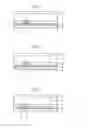
FIG. 5 is a sectional view showing a method of manufacturing a semiconductor device according to a comparative example.
FIG. 6 is a sectional view showing a method of manufacturing a semiconductor device according to Embodiment 2 of the present invention.
FIG. 7 is a sectional view showing a method of manufacturing a semiconductor device according to Embodiment 3 of the present invention.
FIG. 8 is a sectional view showing a method of manufacturing a semiconductor device according to Embodiment 4 of the present invention.
FIG. 9 is a sectional view showing a method of manufacturing a semiconductor device according to Embodiment 5 of the present invention.
FIGS. 10 and 11 are sectional views showing a method of manufacturing a semiconductor device according to Embodiment 6 of the present invention.
FIG. 12 is a sectional view showing a modified example of the method of manufacturing a semiconductor device according to Embodiment 6 of the present invention.
DESCRIPTION OF EMBODIMENTS
A method of manufacturing a semiconductor device according to the embodiments of the present invention will be described with reference to the drawings. The same components will be denoted by the same symbols, and the repeated description thereof may be omitted.
Embodiment 1
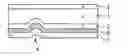
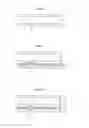
A method of manufacturing a semiconductor device according to Embodiment 1 of the present invention will be described with reference to the drawings. FIGS. 1 to 4 are sectional views showing the method of manufacturing a semiconductor device according to Embodiment 1 of the present invention.
First, as shown in FIG. 1, a p-type layer 2 is formed by implanting a p-type impurity into a front surface of an n−-type Si substrate 1, and an n-type layer 3 is formed by implanting an n-type impurity in a back surface of the substrate 1. A recess 4 (flaw) is formed in the back surface of the Si substrate 1. Subsequently, as shown in FIG. 2, an oxide film 5 is formed on the back surface and in the recess 4. Subsequently, as shown in FIG. 3, the oxide film 5 on the back surface is removed by sputter-etching while the oxide film 5 in the recess 4 is left. It is necessary that at this time part of the oxide film 5 be left at least in an innermost portion of the recess 4. Subsequently, as shown in FIG. 4, an Al—Si film 6 is formed on the back surface. Subsequently, a metal electrode 7 is formed on the Al—Si film 6. The metal electrode 7 is a multilayer electrode.
The advantageous effect of the present embodiment will be described through comparison with a comparative example. FIG. 5 is a sectional view showing a method of manufacturing a semiconductor device according to a comparative example. in the comparative example, the Al—Si film 6 is in direct contact with the Si substrate 1 in an innermost portion of the recess 4. When a reverse voltage is applied to the device, therefore, Al diffuses from the Al—Si film 6 into the Si substrate 1 through the recess 4 to form a p-type layer. Because a depletion layer reaches this p-type layer, a leak current is generated and the withstand voltage of the device is reduced.
On the other hand, in the present embodiment, the oxide film 5 in the recess 4 functions as a protective film for preventing Al from diffusing from the Al—Si film 6 into the Si substrate 1 through the recess 4. Thus, although the recess 4 exists in the back surface of the Si substrate 1, a leak current and a reduction in withstand voltage can be inhibited. Also, separation between the Si substrate 1 and the metal electrode 7 can be inhibited with the Al—Si film 6.
Embodiment 2
FIG. 6 is a sectional view showing a method of manufacturing a semiconductor device according to Embodiment 2 of the present invention. In the present embodiment, an n-type doped polysilicon 8 is formed as a protective film in place of the oxide film 5 in Embodiment 1. In this case, the n-type doped polysilicon S in the recess 4 prevents Al from diffusing the Al—Si film 6 into the Si substrate 1 through the recess 4, thus obtaining the same advantage as in Embodiment 1. Since the n-doped polysilicon 8 is of the n-type, there is a margin for Al that activates the Si substrate 1 into the p-type and energization can be effected even through the recess 4.
Embodiment 3
FIG. 7 is a sectional view showing a method of manufacturing a semiconductor device according to Embodiment 3 of the present invention. In the present embodiment, a phosphosilicate glass 9 is formed as a protective film in place of the oxide film 5 in Embodiment 1. Also in this case, the same advantage as that in Embodiment 1 can be obtained. Since the phosphosilicate glass 9 is of the n-type, there is a margin for Al that activates the Si substrate 1 into the p-type and energization can be effected even through the recess 4.
Embodiment 4
FIG. 8 is a sectional view showing a method of manufacturing a semiconductor device according to Embodiment 4 of the present invention. In the present embodiment, a metal simple substance 10 (titanium) not silicidized is formed as a protective film in place of the oxide film 5 in Embodiment 1.Because the metal simple substance 10 in the recess 4 functions as a barrier metal for preventing diffusion of Al, the same advantage as that in Embodiment 1 can be obtained. The metal simple substance 10 has a good ohmic characteristic with respect to the n-type.
Embodiment 5
FIG. 9 is a sectional view showing a method of manufacturing a semiconductor device according to Embodiment 5 of the present invention. In the present embodiment, a metal film (titanium, cobalt, tungsten or molybdenum) is formed on the back surface and in the recess 4 after the n-type layer 3 is formed. Thereafter, metal suicide 11 (titanium suicide, cobalt suicide, tungsten suicide or molybdenum suicide) is formed by performing annealing. Subsequently, the metal suicide 11 on the back surface is removed by sputter-etching while the metal silicide 11 in the recess 4 is left. Al—Si film 6 and a metal electrode 7 are thereafter formed, as are those in Embodiment 1.
The metal silicide 11 in the recess 4 functions as a protective film for preventing Al from diffusing from the Al—Si film 6 into the Si substrate 1 through the recess 4. The same advantage as that in Embodiment 1 can therefore be obtained. The metal suicide 11 is higher in ohmic characteristic with respect to the n-type layer 3 than the metal simple substance 10 and functions as a barrier metal for preventing diffusion of Al.
Embodiment 6
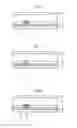
FIGS. 10 and 11 are sectional views showing a method of manufacturing a semiconductor device according to Embodiment 6 of the present invention. First, in the same way as in Embodiment 1, and as shown in FIG. 1, the p-type layer 2 is formed by implanting a p-type impurity into a front surface of the n−-type Si substrate 1, and the n-type layer 3 is formed by implanting an n-type impurity in the back surface of the substrate 1. The recess 4 is formed in the back surface of the Si substrate 1. Subsequently, as shown in FIG. 10, the back surface is recrystallized by laser annealing the back surface while the recess 4 is left, thereby re-forming the n-type layer 3. Subsequently, as shown in FIG. 11, the Al—Si film 6 is formed on the back surface. The metal electrode 7 is formed on the Al—Si film 6.
Prevention of diffusion of Al from the Al—Si film 6 into the Si substrate 1 through the recess 4 is thus enabled. The same advantage as that in Embodiment 1 can therefore be obtained. Also, since the n-type layer 3 can be re-formed, a change in characteristic can be inhibited. While the method of eliminating the recess 4 by melting the back surface by laser application requires a long processing time, the recess 4 is left in the present embodiment to enable shortening the laser annealing processing time and, hence, reducing the manufacturing cost.
FIG. 12 is a sectional view showing a modified example of the method of manufacturing a semiconductor device according to Embodiment 6 of the present invention. Laser annealing is selectively performed only on the recess 4. Recrystallization of a portion including and around the recess 4 can be performed in this way and the advantage of Embodiment 6 can therefore be obtained. Since laser annealing is selectively performed, the laser annealing processing time can be further reduced and a reduction in manufacturing cost can therefore be achieved.
REFERENCE SIGNS LIST
1 Si substrate; 3 n-type layer; 4 recess; 5 oxide film; 6 Al—Si film; 7 metal electrode; 8 n-type doped polysilicon; 9 phosphosilicate glass; 10 metal simple substance; 11 metal suicide
Claims
1. A method of manufacturing a semiconductor device comprising:
forming an n-type layer by implanting an n-type impurity in a back surface of a Si substrate wherein a recess is formed in the back surface;
after forming the n-type layer, forming a protective film on the back surface and in the recess;
removing the protective film on the back surface while the protective film in the recess is left;
after removing the protective film, forming an Al—Si film on the back surface; and
forming a metal electrode on the Al—Si film,
wherein the protective film in the recess prevents Al from diffusing from the Al—Si film into the Si substrate through the recess.
2. The method of manufacturing a semiconductor device according to claim 1, wherein the protective film is an oxide film.
3. The method of manufacturing a semiconductor device according to claim 1, wherein the protective film is an n-type doped polysilicon or a phosphosilicate glass.
4. The method of manufacturing a semiconductor device according to claim 1, wherein the protective film is a metal simple substance.
5. The method of manufacturing a semiconductor device according to claim 1, wherein the protective film is metal silicide.
6. A method of manufacturing a semiconductor device comprising:
forming an n-type layer by implanting an n-type impurity in a back surface of a Si substrate wherein a recess is formed in the back surface;
recrystallizing the back surface by laser annealing the back surface while the recess is left, thereby re-forming the n-type layer;
after the laser annealing, forming an Al—Si film on the back surface; and
forming a metal electrode on the Al—Si film.
7. The method of manufacturing a semiconductor device according to claim 6, wherein the laser annealing is selectively performed on the recess.
Images & Drawings included:
Sources:
- United States Patent and Trademark Office - verify current appl. status at the USPTO↗
Similar patent applications:
Recent applications in this class:
- » 20250239452 2025-07-24
DIRECT NITRATION FOR BACKSIDE POWER DELIVER NETWORK ISOLATION MODULE - » 20240194486 2024-06-13
BACKSIDE AND SIDEWALL METALLIZATION OF SEMICONDUCTOR DEVICES - » 20230187211 2023-06-15
Backside and sidewall metallization of semiconductor devices - » 20210050217 2021-02-18
Method for manufacturing nickel silicide - » 20200388497 2020-12-10
Loading effect reduction through multiple coat-etch processes - » 20190252193 2019-08-15
Loading effect reduction through multiple coat-etch processes - » 20190181010 2019-06-13
Semiconductor device - » 20190088483 2019-03-21
Process of forming electron device having gate electrode - » 20190006182 2019-01-03
Process for producing an intermetallic contact based on Ni on InGaAs - » 20180315606 2018-11-01
Gate cut with high selectivity to preserve interlevel dielectric layer
Recent applications for this Assignee:
- » 20250294680 2025-09-18
POWER MODULE - » 20250293740 2025-09-18
WIRELESS COMMUNICATION SYSTEM - » 20250293196 2025-09-18
SEMICONDUCTOR DEVICE AND MANUFACTURING METHOD THEREOF - » 20250291113 2025-09-18
OPTICAL TERMINATOR, OPTICAL WAVELENGTH FILTER, AND EXTERNAL CAVITY LASER LIGHT SOURCE - » 20250290867 2025-09-18
SEMICONDUCTOR INSPECTION APPARATUS AND METHOD OF MANUFACTURING SEMICONDUCTOR DEVICE - » 20250290765 2025-09-18
INFORMATION PROCESSING DEVICE, INFORMATION PROCESSING METHOD, AND IMAGE PROJECTING SYSTEM - » 20250289592 2025-09-18
SPACE SITUATIONAL AWARENESS BUSINESS DEVICE AND SPACE TRAFFIC BUSINESS DEVICE - » 20250287683 2025-09-11
SEMICONDUCTOR DEVICE - » 20250287624 2025-09-11
POWER SEMICONDUCTOR DEVICE - » 20250287098 2025-09-11
DETECTION DEVICE, CAMERA SYSTEM, DETECTION METHOD, AND STORAGE MEDIUM STORING DETECTION PROGRAM