Method for making contact with a component embedded in a printed circuit board
US20170048984A1
2017-02-16
15/122,114
2015-02-26
✅ Patent granted
US 10,187,997 B2
2019-01-22
WO; PCT/AT2015/050052; 20150226
WO; WO2015/127489; 20150903
Yuriy Semenenko
KPPB LLP
2035-02-26
Abstract:
The invention pertains to a method for the bonding of a component embedded into a printed circuit board exhibiting the following steps:
-
- Provision of a core exhibiting at least one insulating layer and at least one conductor layer applied to the insulating layer,
- Embedding of at least one component into a recess of the insulating layer, wherein the contacts of the component are essentially situated in the plane of an outer surface of the core exhibiting the at least one conductor layer,
- Application of a photoimageable resist onto the one outer surface of the core on which the component is arranged, while filling the spaces between the contacts of the component,
- Clearing of end faces of the contacts and of the areas of the conductor layer covered by the photoimageable resist by exposing and developing the photoimageable resist,
- by application of a semi-additive process, deposition of a layer of conductor material onto the cleared end faces of the contacts and the cleared areas of the conductor layer and formation of a conductor pattern on at least the one outer surface of the core on which the component is arranged, as well as the interconnecting paths between the contacts and the conductor pattern, and
- Removal of the areas of the conductor layer not belonging to the conductor pattern.
Inventors:
- Gerald Weidinger 31 🇦🇹 Leoben, Austria
- Andreas Zluc 35 🇦🇹 Leoben, Austria
- Johannes Stahr 29 🇦🇹 St. Lorenzen, Austria
Assignee:
- AT&S Austia Technologie & Systemtechnik Aktiengesellschaft 1 🇦🇹 Leoben, Austria
- AT&S Austria Technologie & Systemtechnik Aktiengesellschaft 151 🇦🇹 Leoben, Austria
Applicant:
Interested in similar patents?
Get notified when new applications in this technology area are published.
Classification:
H05K1/188 » CPC main
Printed circuits; Printed circuits structurally associated with non-printed electric components associated with components mounted in the printed circuit board, e.g. insert mounted components [IMC]; Components encapsulated in the insulating substrate of the printed circuit or incorporated in internal layers of a multilayer circuit manufactured by mounting on or attaching to a structure having a conductive layer, e.g. a metal foil, such that the terminals of the component are connected to or adjacent to the conductive layer before embedding, and by using the conductive layer, which is patterned after embedding, at least partially for connecting the component
H05K3/064 » CPC further
Apparatus or processes for manufacturing printed circuits in which the conductive material is applied to the surface of the insulating support and is thereafter removed from such areas of the surface which are not intended for current conducting or shielding the conductive material being removed chemically or electrolytically, e.g. by photo-etch process; Etching masks Photoresists
H05K1/18 IPC
Printed circuits Printed circuits structurally associated with non-printed electric components
H05K1/18 IPC
Printed circuits Printed circuits structurally associated with non-printed electric components
H05K3/06 IPC
Apparatus or processes for manufacturing printed circuits in which the conductive material is applied to the surface of the insulating support and is thereafter removed from such areas of the surface which are not intended for current conducting or shielding the conductive material being removed chemically or electrolytically, e.g. by photo-etch process
H05K3/30 » CPC further
Apparatus or processes for manufacturing printed circuits Assembling printed circuits with electric components, e.g. with resistor
H05K3/30 » CPC further
Apparatus or processes for manufacturing printed circuits Assembling printed circuits with electric components, e.g. with resistor
H01L23/5389 » CPC further
Details of semiconductor or other solid state devices; Arrangements for conducting electric current within the device in operation from one component to another, i.e. interconnections, e.g. wires, lead frames the interconnection structure between a plurality of semiconductor chips being formed on, or in, insulating substrates the chips being integrally enclosed by the interconnect and support structures
H01L23/00 IPC
Details of semiconductor or other solid state devices
H01L24/19 » CPC further
Arrangements for connecting or disconnecting semiconductor or solid-state bodies; Methods or apparatus related thereto; Means for bonding being attached to, or being formed on, the surface to be connected, e.g. chip-to-package, die-attach, "first-level" interconnects; Manufacturing methods related thereto; High density interconnect [HDI] connectors; Manufacturing methods related thereto Manufacturing methods of high density interconnect preforms
H01L24/20 » CPC further
Arrangements for connecting or disconnecting semiconductor or solid-state bodies; Methods or apparatus related thereto; Means for bonding being attached to, or being formed on, the surface to be connected, e.g. chip-to-package, die-attach, "first-level" interconnects; Manufacturing methods related thereto; High density interconnect [HDI] connectors; Manufacturing methods related thereto Structure, shape, material or disposition of high density interconnect preforms
H01L2224/73267 » CPC further
Indexing scheme for arrangements for connecting or disconnecting semiconductor or solid-state bodies and methods related thereto as covered by; Means for bonding being of different types provided for in two or more of groups; Location after the connecting process on different surfaces Layer and HDI connectors
H01L2924/15153 » CPC further
Indexing scheme for arrangements or methods for connecting or disconnecting semiconductor or solid-state bodies as covered by; Details of package parts other than the semiconductor or other solid state devices to be connected; Die mounting substrate; Shape the die mounting substrate comprising a recess for hosting the device
H05K3/108 » CPC further
Apparatus or processes for manufacturing printed circuits in which conductive material is applied to the insulating support in such a manner as to form the desired conductive pattern by semi-additive methods; masks therefor
H05K3/108 » CPC further
Apparatus or processes for manufacturing printed circuits in which conductive material is applied to the insulating support in such a manner as to form the desired conductive pattern by semi-additive methods; masks therefor
H05K2201/10674 » CPC further
Indexing scheme relating to printed circuits covered by; Details of components or other objects attached to or integrated in a printed circuit board; Details of electrical connections of non-printed components, e.g. special leads; Components characterised by their electrical contacts Flip chip
H01L23/538 IPC
Details of semiconductor or other solid state devices; Arrangements for conducting electric current within the device in operation from one component to another, i.e. interconnections, e.g. wires, lead frames the interconnection structure between a plurality of semiconductor chips being formed on, or in, insulating substrates
H01L23/13 » CPC further
Details of semiconductor or other solid state devices; Mountings, e.g. non-detachable insulating substrates characterised by the shape
H05K3/10 IPC
Apparatus or processes for manufacturing printed circuits in which conductive material is applied to the insulating support in such a manner as to form the desired conductive pattern
H05K3/10 IPC
Apparatus or processes for manufacturing printed circuits in which conductive material is applied to the insulating support in such a manner as to form the desired conductive pattern
H01L2224/04105 » CPC further
Indexing scheme for arrangements for connecting or disconnecting semiconductor or solid-state bodies and methods related thereto as covered by; Means for bonding being attached to, or being formed on, the surface to be connected, e.g. chip-to-package, die-attach, "first-level" interconnects; Manufacturing methods related thereto; Bonding areas; Manufacturing methods related thereto; Structure, shape, material or disposition of the bonding areas prior to the connecting process Bonding areas formed on an encapsulation of the semiconductor or solid-state body, e.g. bonding areas on chip-scale packages
H01L2224/92244 » CPC further
Indexing scheme for arrangements for connecting or disconnecting semiconductor or solid-state bodies and methods related thereto as covered by; Methods for connecting semiconductor or solid state bodies including different methods provided for in two or more of groups - ; Specific sequence of method steps; Connecting different surfaces of the semiconductor or solid-state body with connectors of different types; Sequential connecting processes the first connecting process involving a layer connector the second connecting process involving a build-up interconnect
Description
The invention pertains to a method for the bonding of a component embedded in a printed circuit board.
The invention furthermore pertains to a printed circuit board with at least one insulated layer and at least one structured conductor layer with conductor paths, with at least one component, which, by means of an adhesive layer, is embedded into a recess of the printed circuit board, with its contacts essentially being situated in the plane of an outer surface of the printed circuit board exhibiting the at least one conductor layer, and with conductive connections between the contacts of the components and the conductor paths of the conductor layer.
The embedding of components, in particular of semiconductor chips, in printed circuit board structures is familiar to the professional, wherein within the scope of the invention, structures are contemplated in which the contacts of the component are essentially situated within one plane at the outer surface of the printed circuit board, also called “surface embedded components”. The electrical contacts of the component must be bonded with a conductor pattern, for which various methods have been applied.
DE 10 2006 009 723 A1, for example, describes a method of embedding a component in a circuit board and of its contacts, in which a first insulating layer with a conductor pattern is applied to a metallic substrate. This is followed by the creation of a window or cut-out for the chip in the first layer, into which the chip—while leaving a gap—is inserted and, using an adhesive, is fixated to the substrate. In doing so, the contacts of the chip are situated on a bonding side facing away from the substrate. Applied on top of this configuration is a photoimageable second insulating layer, which leaves the contact points of the chip cleared, followed by electrical bonding by means of galvanic deposition of a conductor material between the contacts of the chip and the conductor pattern on the first layer. The known method and the resulting product have the disadvantage that in the spacing area between the chip and the adjacent layers a cavity remains, which during the buildup of additional layers may lead to delamination issues.
One objective of this invention is to establish a method with the use of which a conductor pattern in the plane of the contacts, including the respective bondings, can be produced easily and cost-efficiently without the risk of detaching layers.
This objective is achieved with a method of the type referred to above, which according to the invention exhibits the following steps:
-
- a) Provision of a core exhibiting at least one insulating layer and at least one conductor layer applied to the insulating layer,
- b) Embedding of at least one component into a recess of the insulating layer, wherein the contacts of the component are essentially situated within the plane of an outer surface of the printed circuit board exhibiting the at least one conductor layer,
- c) Application of a photoimageable lacquer on the one outer surface of the core on which the component is arranged while filling the spaces between the contacts of the component,
- d) Clearing of end faces of the contacts and of the regions covered by the photoimageable lacquer of the conductor layer by means of exposing and developing the photoimageable lacquer,
- e) using a semi-additive process, deposition of conductor material onto the cleared end faces of the contacts and the cleared regions of the conductor layer and forming of a conductor pattern at least on the one outer surface of the core on which the component is arranged, was well as the interconnecting paths between the contacts and the conductor pattern, and
- f) Removal of the sections of the conductor layer not belonging to the conductor pattern.
Thanks to the invention, embedded components can be “wired” in the same position or plane as the embedding, such that the printed circuit boards can be designed to be thinner and the aforementioned problems of the risk of detachment do not arise.
In doing so, it is recommended for the removal of the sections of the conductor layer in step f) is carried out by flash-etching.
Regarding the additional function of the photoimageable lacquer as a part of the finished printed circuit board, it is advantageous for the photoimageable lacquer used in step c) to be epoxy-based lacquer.
In a particularly advantageous variation of the method according to the invention it may be provided that in step b) the component is embedded into an recess of the core using an adhesive layer, wherein the adhesive layer fully envelops all surfaces of the component—with the exception of those with the contacts—and essentially extends to the plane of the surface of the printed circuit board in which the end faces of the contacts are situated.
In a particularly expedient manner, the recess of the core extends through the conductor layer into the insulating layer.
The stated objectives will also be achieved with a printed circuit board of the above stated type, in which according to the present invention the connections and the conductor paths of the conductor layer are situated in one plane, where the adhesive layer completely envelops all surfaces of the component, except those with the contacts, where the spaces between the contacts of the component are filled with a cured, photoimageable lacquer, and an additional conductor layer is applied to the end faces of the contacts as well as to a conductor layer of the printed circuit board in the area of the conductor paths.
In a preferred embodiment, it is provided that the cured, photoimageable lacquer covers the cleared end faces of the adhesive layer between the outer wall of the component and the inner wall of the recess of the printed circuit board.
In one advanced embodiment of the invention, the printed circuit board again comprises a core exhibiting at least one insulating layer and at least one conductor layer having been applied to the insulating layer, wherein one outer surface of the core having been provided with at least one conductor layer exhibits a recess which extends through the conductor layer into the insulating layer, whereby the component is embedded into the recess of the core by means of an adhesive layer, and wherein the contacts of the component are essentially situated in the plane of the outer surface exhibiting the at least one conductor layer and the recess.
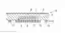
The invention and its further advantages is described in greater detail below based on a sample embodiment of the method and the circuit board, which is illustrated in the drawing. In this drawing show
FIG. 1 in a section through a partial section a core made in the first steps of the method with an embedded component,
FIG. 2 the structure of FIG. 1 after application of a photoimageable lacquer,
FIG. 3 the structure after exposure and development of the photoimageable lacquer,
FIG. 4 the structure after deposition of additional conductive material by application of a semi-additive process and
FIG. 5 the structure of the finished printed circuit board after part of the conductive coatings have been etched away.
The method according to the invention and the inventive printed circuit board will now be explained in reference to the figures. Therein, the term “core” used in the following in the context of the representational description shall be understood to mean a cured prepreg with a conductor layer (copper layer) on at least one surface.
FIG. 1 shows a section of a core 1 consisting of an insulating layer 2, for example consisting of a prepreg material commonly used in the printed circuit board industry, like FR 4, and an upper conductor layer 3 as well as a lower conductor layer 4. At this point it shall be noted that the terms “upper” and “lower” refer to the representation in the drawings only, and are being used for an easier description. Layer thicknesses, for example, are 100 microns for the insulating layer 2 and 1 to 5 microns, typically 2 microns, for upper and lower conductor layer 3 and 4 respectively.
In the core 1, a recess 5 is formed, into which—using an adhesive layer 7—a component 6 is embedded, whereby the layer thickness of this adhesive layer, for example, is 20 to 200 microns. The component 6, a semiconductor chip, for example, carries on an outer surface contacts 8, e.g. copper pads, whereby the adhesive layer 7 envelops all surfaces of the component 6 with the exception of those with the contacts 8, and essentially extends to the plane of the surface of the core 1, in which the end faces of the contacts 8 are situated, in this case, therefore the bottom surface. One possible adhesive, for example, is a solvent-free or low-solvent epoxy resin adhesive with a glass softening point of typically between 120° and 150° C., which will be pressed, filled or injected into the recess 5. After placement of the component 6, this adhesive will be hardened at temperatures of 110° to 150° C.
In a next step, an epoxy-based photoimageable resist 9 is applied at least to the outer surface of the core 1 with the end faces of the contacts 8, with reference being made to FIG. 2. Examples of products and materials suitable for this purpose are the XB7081 lacquer with the trade name Probelec® of the Huntsman Co. or the photoresist SU-8 from Microchem® Corp known from lithographic galvanoplasty (LIGA). As can be seen, the resist 9 is filling all spaces between the contacts 8 of the component 6, and also extends across the lower conductor layer 4.
Thereafter, a photolithographic process commonly used in printed circuit board manufacturing can be used to create the pattern (structuring), starting with exposure using film masking or LDI (Laser Direct Imaging). This is followed by development, obtainment of the patterns after washing-off with suitable chemicals, and the complete curing of the material. Curing is performed by means of conventional curing methods like thermal curing, UV- or IR-curing, application of laser radiation etc. The structuring and the exposure is performed in such manner that the contacts 8, more specifically their end faces, will be cleared, for which purpose reference is made to FIG. 3. This structuring/imaging process is performed such that the cured, photoimageable resist 9 covers the clear end faces of the adhesive layer 7 between the outer wall of the component 6 and the inner wall of the recess 5 of the core 1, and that the lower conductor layer 4 is cleared again.
After this exposure and development, a semi-additive process for applying conductor material, among others, copper is applied according to the desired pattern.
In doing so, a layer 10 of conductor material is applied in the desired areas, in particular for conductor paths, which is deposited also under formation of interconnecting paths 11 starting at the end faces 8 to the desired conductor pattern. The lower conductor layer 4, on the other hand, is amplified in the area of the desired conductor paths or conductor pattern. This result is shown in FIG. 4.
Since bridges 4b continue to exist between the thickened sections of the lower conductor layer 4 through layer 10, which are to form the conductor paths, these bridges 4b and any other undesirable conductor material is removed in an additional step. This is preferably done using so-called “flash etching”, meaning the etching-off of the base copper foil and low-grade removal of the galvanically deposited copper layers. This etching process is performed, for example, with an acidic medium, e.g. HCl with the addition of H2O2 and of stabilizers, wherein the small crystallites of the base film are dissolved significantly faster than the electro-deposited layers, and selective etching is achieved. After this process of removing and etching, the surfaces and spaces between the contacts 9 are cleaned as well and the final conductor paths 12 have emerged and are completely formed, as referenced in FIG. 5, which shows the finished printed circuit board 13 with the embedded and bonded component 6.
In the example shown, only the structuring of the lower conductor layer 4 is described, but it should be clear that the upper conductor layer 3 may also be patterned in the same way. Also possible is the formation of vias (conductive feed-throughs) between the two conductor layers, just as additional insulating and conductor layers may be formed.
Finally, it should be understood that the representations in FIGS. 1 to 5 generally only show detail sections of a larger printed circuit board pattern, and that in practice, a plurality of components may be embedded and connected to conductor patterns at different locations on a printed circuit board.
Claims
1. Method for the bonding of a component embedded into a printed circuit board:
characterized by the following steps:
providing a core exhibiting at least one insulating layer and at least one conductor layer applied to the insulating layer,
embedding at least one component into a recess of the insulating layer, wherein the contacts of the component are essentially situated in the plane of an outer surface of the core exhibiting the at least one conductor layer,
applying a photoimageable resist onto the one outer surface of the core on which the component is arranged, while filling the spaces between the contacts of the component,
clearing end faces of the contacts and of the areas of the conductor layer covered by the photoimageable resist by exposing and developing the photoimageable resist,
depositing a layer of conductor material onto the cleared end faces of the contacts and the cleared areas of the conductor layer and forming a conductor pattern on at least the one outer surface of the core on which the component is arranged, as well as the interconnecting paths between the contacts and the conductor pattern by applying a semi-additive process, and
removing the areas of the conductor layer not belonging to the conductor pattern.
2. Method according to claim 1 characterized in that the removal of the areas of the conductor layer occurs by flash-etching.
3. Method according to claim 1 characterized in that the applied photoimageable resist is an epoxy-based lacquer.
4. Method according to claim 1 characterized in that the embedding of the component using an adhesive layer is embedded into a recess of the core, wherein the adhesive layer fully encloses all surfaces of the component, except for those with the contacts and essentially extends to the plane on the surface of the printed circuit board, in which the end faces of the contacts are situated.
5. Method according to claim 4 characterized in that the recess of the core extends through the conductor layer into the insulating layer.
6. Printed circuit board with at least one insulating layer and at least one patterned conductor layer with conductor paths with at least one component embedded into the insulating layer using an adhesive layer into a recess of the printed circuit board, whose contacts are essentially situated in the plane of an outer surface of the printed circuit board exhibiting the at least one conductor layer and the recess, and with conductive connections between the contacts of the component and conductor paths of the patterned conductor layer, characterized in that
the surfaces of the conductive connections and the conductor paths of the structured conductor layer lie in one plane,
the adhesive layer fully encloses all surfaces of the component, other than those having the contacts,
the spaces between the contacts of the component are filled with a cured, photoimageable resist, and
applied onto the end faces of the contacts and to a conductor layer of the circuit board in the area of the conductor paths is an additional conductor layer.
7. Printed circuit board according to claim 6 characterized in that the cured, photoimageable resist covers the free end faces of the adhesive layer between the outer wall of the component and the inner wall of the recess.
8. Printed circuit board according to claim 6, further comprising a core exhibiting at least one insulating layer and at least one conductor layer applied onto the insulating layer, wherein one outer layer of the core provided with at least one conductor layer exhibits a recess extending through the conductor layer into the insulating layer characterized in that the component, using an adhesive layer, is embedded in the recess of the core, wherein the contacts of the component are essentially situated in the plane of the outer surface of the core exhibiting the at least one conductor layer and the recess.
Images & Drawings included:
Sources:
- United States Patent and Trademark Office - verify current appl. status at the USPTO↗
Similar patent applications:
Recent applications in this class:
- » 20240244755 2024-07-18
Metal Foil for Circuit Board, Metal Foil with Carrier, Copper-Clad Laminate and Printed Circuit Board - » 20240090135 2024-03-14
ELECTRONIC COMPONENT EMBEDDED SUBSTRATE - » 20230397338 2023-12-07
ELECTRONIC COMPONENT - » 20230337363 2023-10-19
METHOD FOR PRODUCING A PRINTED CIRCUIT BOARD, AND PRINTED CIRCUIT BOARD HAVING AT LEAST ONE EMBEDDED ELECTRONIC COMPONENT - » 20230140708 2023-05-04
Electronic component embedded substrate - » 20230038270 2023-02-09
Protection Structure for an Aperture for an Optical Component Embedded Within a Component Carrier - » 20220022323 2022-01-20
Driver board assemblies and methods of forming a driver board assembly - » 20220015238 2022-01-13
Embedded circuit board and method of manufacturing same - » 20220007512 2022-01-06
Processor interposer and electronic system including the processor interposer - » 20210329788 2021-10-21
Method for manufacturing an electronic module and electronic module
Recent applications for this Assignee:
- » 20250227850 2025-07-10
Method for Embedding a Component in a Printed Circuit Board - » 20250081350 2025-03-06
COMPONENT CARRIER - » 20230189448 2023-06-15
Printed circuit board having embedded component - » 20230135105 2023-05-04
Component Embedded in Component Carrier and Having an Exposed Side Wall - » 20230134610 2023-05-04
Component carrier for microwave applications with stack pieces interconnected at an electrically conductive connection interface - » 20230035496 2023-02-02
Component carrier having dielectric layer with conductively filled through holes tapering in opposite directions - » 20220377896 2022-11-24
Component carrier with a magnetic element and a manufacturing method - » 20220346229 2022-10-27
Component carrier - » 20220319943 2022-10-06
Embedding methods for fine-pitch components and corresponding component carriers - » 20220310428 2022-09-29
Component carrier with gap around component core and filled with first material in bottom portion and with second material in top portion