Stacked modular architecture high-resolution thermal chip camera
US20170070685A1
2017-03-09
14/845,861
2015-09-04
✅ Patent granted
US 9,787,914 B2
2017-10-10
-
-
David Porta | Gisselle Gutierrez
Maine Cernota & Rardin
2036-06-14
Abstract:
An uncooled high-resolution 12 micron pixel pitch 3D-stacked component thermal camera including an electronics board, a camera circuit card assembly (CCA) with an application-specific integrated circuit (ASIC), a synchronous dynamic random access memory (SDRAM), flash memory, a spacer, a wafer level packaged Focal Plane Array (FPA) wafer with a lens housing attach ring on the FPA, and a window.
Inventors:
- Louise C. Sengupta 41 🇺🇸 Ellicott City, MD, United States
- Richard J. Blackwell, JR. 4 🇺🇸 Dracut, MA, United States
- Mihir D. Boal 4 🇺🇸 Nashua, NH, United States
- Pierre-Alain S. Auroux 10 🇺🇸 Rockville, MD, United States
- Don A. HARRIS 8 🇺🇸 Columbia, MD, United States
- Evan A. Binkerd 1 🇺🇸 Merrimack, NH, United States
- Jeffrey F. Bryant 2 🇺🇸 Amherst, NH, United States
- Donald D. McManus 1 🇺🇸 Bedford, NH, United States
Assignee:
- BAE Systems Information and Electronic Systems Integration Inc. 1,774 🇺🇸 Nashua, NH, United States
Applicant:
Interested in similar patents?
Get notified when new applications in this technology area are published.
Classification:
H01L27/115 IPC
Devices consisting of a plurality of semiconductor or other solid-state components formed in or on a common substrate including semiconductor components specially adapted for rectifying, oscillating, amplifying or switching and having at least one potential-jump barrier or surface barrier; including integrated passive circuit elements with at least one potential-jump barrier or surface barrier the substrate being a semiconductor body including a plurality of individual components in a repetitive configuration including field-effect components; Read-only memory structures [ROM] and multistep manufacturing processes therefor Electrically programmable read-only memories; Multistep manufacturing processes therefor
H01L21/78 » CPC further
Processes or apparatus adapted for the manufacture or treatment of semiconductor or solid state devices or of parts thereof; Manufacture or treatment of devices consisting of a plurality of solid state components formed in or on a common substrate or of parts thereof; Manufacture of integrated circuit devices or of parts thereof; Manufacture or treatment of devices consisting of a plurality of solid state components or integrated circuits formed in, or on, a common substrate with subsequent division of the substrate into plural individual devices
H01L27/10805 » CPC further
Devices consisting of a plurality of semiconductor or other solid-state components formed in or on a common substrate including semiconductor components specially adapted for rectifying, oscillating, amplifying or switching and having at least one potential-jump barrier or surface barrier; including integrated passive circuit elements with at least one potential-jump barrier or surface barrier the substrate being a semiconductor body including a plurality of individual components in a repetitive configuration including field-effect components; Dynamic random access memory structures with one-transistor one-capacitor memory cells
H01L27/1469 » CPC further
Devices consisting of a plurality of semiconductor or other solid-state components formed in or on a common substrate including semiconductor components sensitive to infra-red radiation, light, electromagnetic radiation of shorter wavelength or corpuscular radiation and specially adapted either for the conversion of the energy of such radiation into electrical energy or for the control of electrical energy by such radiation; Devices controlled by radiation; Imager structures; Processes or apparatus peculiar to the manufacture or treatment of these devices or parts thereof Assemblies, i.e. hybrid integration
H01L27/14618 » CPC further
Devices consisting of a plurality of semiconductor or other solid-state components formed in or on a common substrate including semiconductor components sensitive to infra-red radiation, light, electromagnetic radiation of shorter wavelength or corpuscular radiation and specially adapted either for the conversion of the energy of such radiation into electrical energy or for the control of electrical energy by such radiation; Devices controlled by radiation; Imager structures; Structural or functional details thereof Containers
H01L27/14625 » CPC further
Devices consisting of a plurality of semiconductor or other solid-state components formed in or on a common substrate including semiconductor components sensitive to infra-red radiation, light, electromagnetic radiation of shorter wavelength or corpuscular radiation and specially adapted either for the conversion of the energy of such radiation into electrical energy or for the control of electrical energy by such radiation; Devices controlled by radiation; Imager structures; Structural or functional details thereof Optical elements or arrangements associated with the device
H01L27/14632 » CPC further
Devices consisting of a plurality of semiconductor or other solid-state components formed in or on a common substrate including semiconductor components sensitive to infra-red radiation, light, electromagnetic radiation of shorter wavelength or corpuscular radiation and specially adapted either for the conversion of the energy of such radiation into electrical energy or for the control of electrical energy by such radiation; Devices controlled by radiation; Imager structures; Structural or functional details thereof Wafer-level processed structures
H01L27/14634 » CPC further
Devices consisting of a plurality of semiconductor or other solid-state components formed in or on a common substrate including semiconductor components sensitive to infra-red radiation, light, electromagnetic radiation of shorter wavelength or corpuscular radiation and specially adapted either for the conversion of the energy of such radiation into electrical energy or for the control of electrical energy by such radiation; Devices controlled by radiation; Imager structures; Structural or functional details thereof Assemblies, i.e. Hybrid structures
H01L27/14636 » CPC further
Devices consisting of a plurality of semiconductor or other solid-state components formed in or on a common substrate including semiconductor components sensitive to infra-red radiation, light, electromagnetic radiation of shorter wavelength or corpuscular radiation and specially adapted either for the conversion of the energy of such radiation into electrical energy or for the control of electrical energy by such radiation; Devices controlled by radiation; Imager structures; Structural or functional details thereof Interconnect structures
H01L27/14685 » CPC further
Devices consisting of a plurality of semiconductor or other solid-state components formed in or on a common substrate including semiconductor components sensitive to infra-red radiation, light, electromagnetic radiation of shorter wavelength or corpuscular radiation and specially adapted either for the conversion of the energy of such radiation into electrical energy or for the control of electrical energy by such radiation; Devices controlled by radiation; Imager structures; Processes or apparatus peculiar to the manufacture or treatment of these devices or parts thereof Process for coatings or optical elements
H01L27/14687 » CPC further
Devices consisting of a plurality of semiconductor or other solid-state components formed in or on a common substrate including semiconductor components sensitive to infra-red radiation, light, electromagnetic radiation of shorter wavelength or corpuscular radiation and specially adapted either for the conversion of the energy of such radiation into electrical energy or for the control of electrical energy by such radiation; Devices controlled by radiation; Imager structures; Processes or apparatus peculiar to the manufacture or treatment of these devices or parts thereof Wafer level processing
H04N5/2257 » CPC further
Details of television systems; Studio circuitry; Studio devices; Studio equipment ; Cameras comprising an electronic image sensor, e.g. digital cameras, video cameras, TV cameras, video cameras, camcorders, webcams, camera modules for embedding in other devices, e.g. mobile phones, computers or vehicles; Television cameras ; Cameras comprising an electronic image sensor, e.g. digital cameras, video cameras, camcorders, webcams, camera modules specially adapted for being embedded in other devices, e.g. mobile phones, computers or vehicles Mechanical and electrical details of cameras or camera modules for embedding in other devices
H01L27/146 IPC
Devices consisting of a plurality of semiconductor or other solid-state components formed in or on a common substrate including semiconductor components sensitive to infra-red radiation, light, electromagnetic radiation of shorter wavelength or corpuscular radiation and specially adapted either for the conversion of the energy of such radiation into electrical energy or for the control of electrical energy by such radiation; Devices controlled by radiation Imager structures
H01L27/108 IPC
Devices consisting of a plurality of semiconductor or other solid-state components formed in or on a common substrate including semiconductor components specially adapted for rectifying, oscillating, amplifying or switching and having at least one potential-jump barrier or surface barrier; including integrated passive circuit elements with at least one potential-jump barrier or surface barrier the substrate being a semiconductor body including a plurality of individual components in a repetitive configuration including field-effect components Dynamic random access memory structures
H04N5/225 IPC
Details of television systems; Studio circuitry; Studio devices; Studio equipment ; Cameras comprising an electronic image sensor, e.g. digital cameras, video cameras, TV cameras, video cameras, camcorders, webcams, camera modules for embedding in other devices, e.g. mobile phones, computers or vehicles Television cameras ; Cameras comprising an electronic image sensor, e.g. digital cameras, video cameras, camcorders, webcams, camera modules specially adapted for being embedded in other devices, e.g. mobile phones, computers or vehicles
H04N5/33 » CPC main
Details of television systems; Transforming light or analogous information into electric information Transforming infra-red radiation
Description
STATEMENT OF GOVERNMENT INTEREST
The invention was made with United States Government support under Contract No. HR0011-11-C-0126 awarded by the Defense Advanced Research Projects Agency (DARPA). The United States Government has certain rights in this invention.
FIELD OF THE INVENTION
The invention relates to uncooled thermal imagers and more particularly relates to high-resolution thermal chip cameras.
BACKGROUND OF THE INVENTION
Traditional uncooled thermal imager cost is prohibitive for mass-production. In addition, the size, weight, power requirements (and cost) of these imagers may not be well-suited for Unmanned Arial Vehicles (UAV) and man-portable applications.
A need exists for uncooled cameras which are small, light-weight, power efficient, and inexpensive enough to be well-suited for UAV and man portable applications.
SUMMARY OF THE INVENTION
An embodiment provides an uncooled high-resolution 12 micron pixel pitch 3D-stacked component thermal camera device comprising a camera circuit card assembly (CCA) comprising an application-specific integrated circuit (ASIC); a synchronous dynamic random access memory (SDRAM); a flash memory wafer; and a wafer level packaged Focal Plane Array (FPA) wafer. In embodiments, the CCA comprises a small circuit board with the FPA on one side, the ASIC, the SDRAM memory and the flash memory and other supporting circuits and output connector on the back side of the CCA. In other embodiments, the configuration of the camera comprises the FPA and electronics adjacent to each other on a same side of a circuit board of the CCA. In subsequent embodiments, the wafer level packaged FPA comprises a focal plane and a window, a lens integrated with the camera by a lens housing attach ring on the FPA, and a spacer between the SDRAM memory and flash memory. For additional embodiments, the CCA comprises Surface Mount Technology (SMT) devices. In another embodiment, the camera operates at 15 Hz, 30 Hz, and 60 Hz with a slow frame rate of about 7.5 Hz to about 8.33 Hz. For a following embodiment, the ASIC, the SDRAM, and the flash memory wafers comprise full thickness substrates. In subsequent embodiments, the ASIC, the SDRAM, and the flash memory wafers are thinned. In additional embodiments, at least one of the ASIC, the SDRAM, and the flash memory has a full thickness substrate and at least one is thinned.
Another embodiment provides a method for preparing a bare die for a 12 micron pixel pitch uncooled high-resolution thermal camera using 3D-stacking implementation comprising dicing an application-specific integrated circuit (ASIC) wafer; dicing synchronous dynamic random access memory (SDRAM) wafer; dicing flash wafer; dicing a wafer level packaged Focal Plane Array (FPA) wafer; assembling a circuit card assembly (CCA); die attaching the ASIC; die attaching the SDRAM; die attaching a spacer; die attaching the flash; wire bonding the SDRAM to the ASIC; wire bonding the flash to the ASIC; wire bonding the ASIC to the CCA; wire bonding the SDRAM to the CCA; wire bonding the flash to the CCA; die attaching the FPA; wire bonding the FPA to the CCA; and filling backside whereby the ASIC stack wire bonds are protected. In included embodiments, the CCA assembly comprises attaching standard Surface Mount Technology (SMT) devices. In yet further embodiments, the camera operates at 15 Hz, 30 Hz, and 60 Hz. In related embodiments, the diced ASIC wafer, the diced SDRAM wafer, and the diced flash wafer are full thickness substrates. For further embodiments, the diced ASIC wafer, the diced SDRAM wafer, and the diced flash wafer are thinned. In ensuing embodiments, at least one of the diced ASIC wafer, the diced SDRAM wafer, and the diced flash wafer has a full thickness substrate and at least one is thinned. For yet further embodiments, the CCA comprises a small circuit board with the FPA on one side, the ASIC, the SDRAM memory and the flash memory and other supporting circuits and output connector on a back side of the CCA. For more embodiments, a configuration of the camera comprises the FPA and electronics adjacent to each other on a same side of a circuit board of the CCA. In continued embodiments, the wafer level packaged FPA comprises a focal plane and a window, a lens integrated with the camera by a lens housing attach ring on the FPA, and a spacer between the SDRAM memory and flash memory. For additional embodiments, the camera operates with a slow frame rate of about 7.5 Hz to about 8.33 Hz.
A yet further embodiment provides an uncooled 12 micron pixel pitch high-resolution thermal camera system using 3D-stacking comprising a camera circuit card assembly (CCA); an application-specific integrated circuit (ASIC), the ASIC comprising an imaging engine to operate a Focal Plane Array (FPA) and provide pixel corrections and calibration; a synchronous dynamic random access memory (SDRAM); a flash memory wafer, wherein the SDRAM memory and the flash memory are stacked on the ASIC; and a wafer level packaged FPA wafer comprising the FPA, wherein the FPA comprises alignment pixels and buffer pixels and a partition architecture; a lens comprising an f-number of about 1.2, a Field Of View (FOV) of about 42°×26°, and an Instantaneous Field Of View (IFOV) of about 400 μrad; a Cameralink input output adapter; a Mobile Industry Processor Interface (MIPI) format adapter; and dual row biasing for large arrays whereby adequate pulse time and sensitivity are maintained.
BRIEF DESCRIPTION OF THE DRAWINGS
FIG. 1 is a perspective view of a VGA FPA configured in accordance with an embodiment of the invention.
FIG. 2 shows perspective and exploded views of a Stacked Modular Architecture High-Resolution Thermal (SMART) chip camera configured in accordance with an embodiment of the invention.
FIG. 3 shows front and rear elevational views of the circuit card assembly (CCA) board configured in accordance with an embodiment of the invention.
FIG. 4 shows front and rear views of the CCA board and a perspective view of the lens mount configured in accordance with an embodiment of the invention.
FIG. 5 shows views of the integration of the chip camera with a cell phone configured in accordance with an embodiment of the invention.
FIG. 6 shows front and rear views of the integration of the chip camera with a flex cable configured in accordance with an embodiment of the invention.
FIG. 7 depicts a CHIP camera method configured in accordance with an embodiment of the invention.
DETAILED DESCRIPTION
The features and advantages described herein are not all-inclusive and, in particular, many additional features and advantages will be apparent to one of ordinary skill in the art in view of the drawings, specification, and claims. Moreover, it should be noted that the language used in the specification has been selected principally for readability and instructional purposes, and not to limit in any way the scope of the inventive subject matter. The invention is susceptible of many embodiments. What follows is illustrative, but not exhaustive, of the scope of the invention.
In one embodiment of the invention, the SMART chip camera costs less than $500, presents a volume smaller than 3.5 cubic centimeters, weighs less than 25 grams, and consumes less than 500 milliwatts. Wafer-level technologies are leveraged at multiple levels to accomplish superior achievements such as packaging of the bolometers and calibration of the units. In addition, the electronics board is rendered more compact and less power consumptive by using 3D-stacking implementation. Finally, the IR camera is compatible with Android-based cell phones.
FIG. 1 shows a perspective view 100 of the Low Cost Thermal Imager-Manufacturing (LCTI-M) sensor (without lens). For comparison, penny 105 is shown beside sensor 110. The top side is the wafer level packaged VGA FPA. The back side contains an ASIC imaging engine, memory, supporting electronics, and system flex connector. This module, with a very compact wafer-scale compatible f/1.2 lens, has been demonstrated and integrated into a commercial cell phone displaying the IR image on the cell phone display using a custom Android application. The basic VGA FPA was available early in the LCTI-M program and has seen early insertions into several applications requiring uncooled cameras which are small, light-weight, power efficient, and inexpensive.
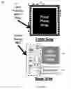
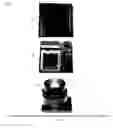
FIG. 2 shows perspective and exploded views of a SMART chip camera 200. Depicted are flash 205, spacer 210, SDRAM 215, ASIC 220, focal plane 225, window 230, lens housing 235, and perspective view 240. In a camera embodiment, significant components include 1) wafer level packaged FPA (focal plane and window), 2) ASIC for imaging engine to operate FPA and provide pixel corrections/calibration, 3) memory (SDRAM and flash) stacked on ASIC (or in close proximity), 4) small circuit board with FPA on one side and ASIC/memory and other supporting circuits and output connector on back side, 5) lens integrated with 1-4, 6) an alternate configuration with FPA and electronics adjacent to each other on the same side of the circuit board.
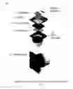
FIG. 3 shows front and rear elevation views 300 of the circuit card assembly (CCA) board. Depicted components include lens housing attach ring 305, focal plane array 310 on front side, and power supply SMT 315, ASIC memory stack 320, and connector 325 on back side.
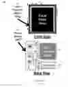
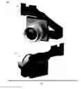
FIG. 4 shows the assembly of a prototype 400. Depicted are front side of the wafer level packaged FPA circuit board 405; back side of the circuit board with stacked ASIC/memory, connector, and supporting circuits 410; and compact lens for mounting on the front side of the CCA 415. Embodiments have other lens mount methods.
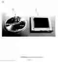
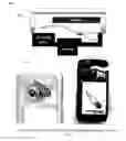
FIG. 5 shows the physical integration of the SMART chip camera with a cell phone 500. Depicted are component arrangement 505; lens-side perspective view 510; and cell phone device internals 515.
FIG. 6 shows views 600 of the integration of the SMART chip camera with a flex cable showing a service loop. Depicted are view from the lens front side 605 and view from the lens rear side 610. The flex cable has a chip to convert sensor output to Mobile Industry Processor Interface (MIPI) format (to interface with phone processors or other MIPI devices).
FIG. 7 presents device manufacturing steps 700. CCA manufacturing steps comprise bare die preparation 705; ASIC wafer diced 710; SDRAM wafer diced 715; flash wafer diced 720 (these may be thinned or full thickness substrates); wafer level packaged Focal Plane Array wafer diced 725; CCA Assembly 730 comprising: attach standard Surface Mount Technology (SMT) devices 735 (i.e. power supply and decoupling capacitors); die attach ASIC 740; die attach SDRAM 745; die attach spacer 750; and die attach flash 755; wire bond SDRAM to ASIC 760; wire bond flash to ASIC 765; die attach FPA 770; wire bond FPA to CCA 775; and fill back side to protect ASIC stack wirebonds 780.
The foregoing description of the embodiments of the invention has been presented for the purposes of illustration and description. It is not intended to be exhaustive or to limit the invention to the precise form disclosed. Each and every page of this submission, and all contents thereon, however characterized, identified, or numbered, is considered a substantive part of this application for all purposes, irrespective of form or placement within the application. This specification is not intended to be exhaustive or to limit the invention to the precise form disclosed. Many modifications and variations are possible in light of this disclosure. Other and various embodiments will be readily apparent to those skilled in the art, from this description, figures, and the claims that follow. It is intended that the scope of the invention be limited not by this detailed description, but rather by the claims appended hereto.
Claims
What is claimed is:1. An uncooled high-resolution 12 micron pixel pitch 3D-stacked component thermal camera device comprising:
a camera circuit card assembly (CCA) comprising:
an application-specific integrated circuit (ASIC);
a synchronous dynamic random access memory (SDRAM);
a flash memory wafer; and
a wafer level packaged Focal Plane Array (FPA) wafer.
2. The system of claim 1, wherein said CCA comprises a small circuit board with said FPA on one side, said ASIC, said SDRAM memory and said flash memory and other supporting circuits and output connector on a back side of said CCA.
3. The system of claim 1, wherein configuration of said camera comprises said FPA and electronics adjacent to each other on a same side of a circuit board of said CCA.
4. The system of claim 1, wherein said wafer level packaged FPA comprises a focal plane and a window, a lens integrated with said camera by a lens housing attach ring on said FPA, and a spacer between said SDRAM memory and flash memory.
5. The system of claim 1, wherein said CCA comprises Surface Mount Technology (SMT) devices.
6. The system of claim 1, wherein said camera operates at 15 Hz, 30 Hz, and 60 Hz with a slow frame rate of about 7.5 Hz to about 8.33 Hz.
7. The system of claim 1, wherein said ASIC, said SDRAM, and said flash memory wafers comprise full thickness substrates.
8. The system of claim 1, wherein said ASIC, said SDRAM, and said flash memory wafers are thinned.
9. The system of claim 1, wherein at least one of said ASIC, said SDRAM, and said flash memory has a full thickness substrate and at least one is thinned.
10. A method for preparing a bare die for a 12 micron pixel pitch uncooled high-resolution thermal camera using 3D-stacking implementation comprising:
dicing an application-specific integrated circuit (ASIC) wafer;
dicing synchronous dynamic random access memory (SDRAM) wafer;
dicing flash wafer;
dicing a wafer level packaged Focal Plane Array (FPA) wafer;
assembling a circuit card assembly (CCA);
die attaching said ASIC;
die attaching said SDRAM;
die attaching a spacer;
die attaching said flash;
wire bonding said SDRAM to said ASIC;
wire bonding said flash to said ASIC;
wire bonding said ASIC to said CCA;
wire bonding said SDRAM to said CCA;
wire bonding said flash to said CCA;
die attaching said FPA;
wire bonding said FPA to said CCA; and
filling backside whereby said ASIC stack wire bonds are protected.
11. The method of claim 10, wherein said CCA assembly comprises:
attaching standard Surface Mount Technology (SMT) devices.
12. The method of claim 10, wherein said camera operates at 15 Hz, 30 Hz, and 60 Hz.
13. The method of claim 10, wherein said diced ASIC wafer, said diced SDRAM wafer, and said diced flash wafer are full thickness substrates.
14. The method of claim 10, wherein said diced ASIC wafer, said diced SDRAM wafer, and said diced flash wafer are thinned.
15. The method of claim 10, wherein at least one of said diced ASIC wafer, said diced SDRAM wafer, and said diced flash wafer has a full thickness substrate and at least one is thinned.
16. The method of claim 10, wherein said CCA comprises a small circuit board with said FPA on one side, said ASIC, said SDRAM memory and said flash memory and other supporting circuits and output connector on a back side of said CCA.
17. The method of claim 10, wherein a configuration of said camera comprises said FPA and electronics adjacent to each other on a same side of a circuit board of said CCA.
18. The method of claim 10, wherein said wafer level packaged FPA comprises a focal plane and a window, a lens integrated with said camera by a lens housing attach ring on said FPA, and a spacer between said SDRAM memory and flash memory.
19. The method of claim 10, wherein said camera operates with a slow frame rate of about 7.5 Hz to about 8.33 Hz.
20. An uncooled 12 micron pixel pitch high-resolution thermal camera system using 3D-stacking comprising:
a camera circuit card assembly (CCA);
an application-specific integrated circuit (ASIC), said ASIC comprising an imaging engine to operate a Focal Plane Array (FPA) and provide pixel corrections and calibration;
a synchronous dynamic random access memory (SDRAM);
a flash memory wafer, wherein said SDRAM memory and said flash memory are stacked on said ASIC; and
a wafer level packaged FPA wafer comprising said FPA, wherein said ii FPA comprises alignment pixels and buffer pixels and a partition architecture;
a lens comprising an f-number of about 1.2, a Field Of View (FOV) of about 42°×26°, and an Instantaneous Field Of View (IFOV) of about 400 μrad;
a Cameralink input output adapter;
a Mobile Industry Processor Interface (MIPI) format adapter; and
dual row biasing for large arrays whereby adequate pulse time and sensitivity are maintained.
Images & Drawings included:

Sources:
- United States Patent and Trademark Office - verify current appl. status at the USPTO↗
Recent applications in this class:
- » 20250211705 2025-06-26
Thermal Imaging Camera - » 20250088604 2025-03-13
IMAGING AND DISPLAY SYSTEM COMBINING IR AND COLOR VIDEO STREAMS - » 20250071233 2025-02-27
Light-Folded Projector - » 20240430380 2024-12-26
SYSTEM AND METHOD FOR PROVISIONING A FACIAL RECOGNITION-BASED SYSTEM FOR CONTROLLING ACCESS TO A BUILDING - » 20240333866 2024-10-03
EVENT-BASED IR CAMERA - » 20240314266 2024-09-19
METHOD FOR DETERMINING HEAT AND REFLECTED HEAT IN THERMAL IMAGE - » 20240236261 2024-07-11
OPTICAL SENSOR HAVING OPAQUE LAYER - » 20240223719 2024-07-04
Mobile gas and chemical imaging camera - » 20240214514 2024-06-27
REFRIGERATION SYSTEM WITH TEMPERATURE MONITORING - » 20240187546 2024-06-06
Uncooled thermal imager
Recent applications for this Assignee:
- » 20250293737 2025-09-18
RECONFIGURABLE SPACE TIME AND SPACE FREQUENCY ADAPTIVE PROCESSING - » 20250291062 2025-09-18
GLOBAL NAVIGATION SATELLITE SYSTEM (GNSS) SPOOFER PROTECTION - » 20250290801 2025-09-18
COMPACT APPARATUS FOR NON-CONTACT TEMPERATURE SENSING OF ROTATING ELEMENTS - » 20250283245 2025-09-11
TRANSPARENT HORIZONTAL GRADIENT FREEZE APPARATUS WITH REGULATED GROWTH RATE - » 20250277910 2025-09-04
MULTI-STAGE MULTI-BURST SIGNAL ACQUISITION - » 20250277652 2025-09-04
EXTENDED FIRE MUX CONTROL WITH POLLING SOURCE - » 20250277640 2025-09-04
DUAL USE MAGAZINE IDENTIFICATION WIRE WITH POWER ROUTING - » 20250273862 2025-08-28
INTEGRATED ANTENNA AND TETHER - » 20250271578 2025-08-28
IONOSPHERIC DELAY MEASUREMENT FOR REDUCED GPS POWER CONSUMPTION - » 20250271546 2025-08-28
ELECTRONIC WARFARE SYSTEM HAVING OPTIMIZED MULTIPLE SCAN SCHEDULES