Display panel
US20170123264A1
2017-05-04
15/009,547
2016-01-28
✅ Patent granted
US 9,857,619 B2
2018-01-02
-
-
Tan N Tran
Andrew C. Cheng
2036-01-28
Abstract:
The present disclosure discloses a display panel, including a color filter plate substrate and an array substrate; the color filter plate substrate includes a black matrix and a protective layer; the color filter plate substrate and the array substrate are disposed opposite; the protective layer is disposed on a side of the black matrix oriented to the array substrate in a laser incidence region during laser repair. The protective layer is disposed on a side of the black matrix oriented to the array substrate in a laser incidence region during laser repair according to the disclosure, therefore, the preventive layer can protect the black matrix during laser repair from forming a through-hole on the black matrix that can leak light.
Inventors:
- Yafeng LI 5 🇨🇳 Shenzhen, China
- Xiangyi PENG 1 🇨🇳 Shenzhen, China
- Yafeng Li 6 🇨🇳 Guangdong, China
- Xiangyi Peng 1 🇨🇳 Guangdong, China
Assignee:
- Wuhan China Star Optoelectronics Technology Co., Ltd. 1,118 🇨🇳 Wuhan, Hubei, China
- WUHAN CHINA STAR OPTOELECTRONICS TECHNOLOGY CO., LTD. 817 🇨🇳 Wuhan, China
Applicant:
Interested in similar patents?
Get notified when new applications in this technology area are published.
Classification:
G02F1/13394 » CPC further
Devices or arrangements for the control of the intensity, colour, phase, polarisation or direction of light arriving from an independent light source, e.g. switching, gating or modulating; Non-linear optics for the control of the intensity, phase, polarisation or colour based on liquid crystals, e.g. single liquid crystal display cells; Constructional arrangements; Operation of liquid crystal cells; Circuit arrangements; Constructional arrangements; Manufacturing methods; Gaskets; Spacers; Sealing of cells spacers regularly patterned on the cell subtrate, e.g. walls, pillars
G02F1/136259 » CPC further
Devices or arrangements for the control of the intensity, colour, phase, polarisation or direction of light arriving from an independent light source, e.g. switching, gating or modulating; Non-linear optics for the control of the intensity, phase, polarisation or colour based on liquid crystals, e.g. single liquid crystal display cells; Constructional arrangements; Operation of liquid crystal cells; Circuit arrangements; Liquid crystal cells structurally associated with a semi-conducting layer or substrate, e.g. cells forming part of an integrated circuit; Active matrix addressed cells Repairing; Defects
G02F1/136286 » CPC further
Devices or arrangements for the control of the intensity, colour, phase, polarisation or direction of light arriving from an independent light source, e.g. switching, gating or modulating; Non-linear optics for the control of the intensity, phase, polarisation or colour based on liquid crystals, e.g. single liquid crystal display cells; Constructional arrangements; Operation of liquid crystal cells; Circuit arrangements; Liquid crystal cells structurally associated with a semi-conducting layer or substrate, e.g. cells forming part of an integrated circuit; Active matrix addressed cells Wiring, e.g. gate line, drain line
H01L27/14 IPC
Devices consisting of a plurality of semiconductor or other solid-state components formed in or on a common substrate including semiconductor components sensitive to infra-red radiation, light, electromagnetic radiation of shorter wavelength or corpuscular radiation and specially adapted either for the conversion of the energy of such radiation into electrical energy or for the control of electrical energy by such radiation
G02F1/1335 IPC
Devices or arrangements for the control of the intensity, colour, phase, polarisation or direction of light arriving from an independent light source, e.g. switching, gating or modulating; Non-linear optics for the control of the intensity, phase, polarisation or colour based on liquid crystals, e.g. single liquid crystal display cells; Constructional arrangements; Operation of liquid crystal cells; Circuit arrangements; Constructional arrangements; Manufacturing methods Structural association of cells with optical devices, e.g. polarisers or reflectors
G02F1/1362 IPC
Devices or arrangements for the control of the intensity, colour, phase, polarisation or direction of light arriving from an independent light source, e.g. switching, gating or modulating; Non-linear optics for the control of the intensity, phase, polarisation or colour based on liquid crystals, e.g. single liquid crystal display cells; Constructional arrangements; Operation of liquid crystal cells; Circuit arrangements; Liquid crystal cells structurally associated with a semi-conducting layer or substrate, e.g. cells forming part of an integrated circuit Active matrix addressed cells
G02F1/1339 IPC
Devices or arrangements for the control of the intensity, colour, phase, polarisation or direction of light arriving from an independent light source, e.g. switching, gating or modulating; Non-linear optics for the control of the intensity, phase, polarisation or colour based on liquid crystals, e.g. single liquid crystal display cells; Constructional arrangements; Operation of liquid crystal cells; Circuit arrangements; Constructional arrangements; Manufacturing methods Gaskets; Spacers; Sealing of cells
G02F1/1368 » CPC further
Devices or arrangements for the control of the intensity, colour, phase, polarisation or direction of light arriving from an independent light source, e.g. switching, gating or modulating; Non-linear optics for the control of the intensity, phase, polarisation or colour based on liquid crystals, e.g. single liquid crystal display cells; Constructional arrangements; Operation of liquid crystal cells; Circuit arrangements; Liquid crystal cells structurally associated with a semi-conducting layer or substrate, e.g. cells forming part of an integrated circuit; Active matrix addressed cells in which the switching element is a three-electrode device
Description
FIELD OF THE INVENTION
The present disclosure relates to a display technology field, and more particularly to a display panel.
BACKGROUND OF THE INVENTION
As well known, laser technology is the most common technique in low temperature poly-silicon (LTPS) technology, which is widely applied in point repair, line repair and laser annealing, however, during repair, the laser can penetrate an array substrate due to high intensity of the laser and impact on a black matrix on a color filter plate substrate, which makes a through-hole on the black matrix that can leak light.
SUMMARY OF THE INVENTION
The technical issue that the embodiment of the present invention solves is to provide a display panel that can prevent light leakage of a black matrix due to laser repair.
The present disclosure provides a display panel to solve the technical problem above, including: a color filter plate substrate and an array substrate;the color filter plate substrate includes a black matrix and a protective layer; the color filter plate substrate and the array substrate are disposed opposite;the protective layer is disposed on a side of the black matrix oriented to the array substrate in a laser incidence region during laser repair.
The protective layer is an organic material layer.
The protective layer is formed by a plurality of alternate spacer disposed on the black matrix layer.
The array substrate includes a thin film transistor (TFT) and a metal wire, the spacer is disposed on a black matrix of a position corresponding to the TFT and metal wire.
The spacer is also disposed on a black matrix of a position corresponding to a peripheral region of the array substrate, a contact area of the spacer corresponding to the TFT and metal wire, and the black matrix is larger than a contact area of the spacer corresponding to the peripheral region of the array substrate and the black matrix.
Distribution of the each spacer corresponding to the TFT and metal wire is more compact than that of the each spacer corresponding to the peripheral region of the array substrate.
A contact area of the spacer corresponding to the TFT and metal wire, and the black matrix is larger than a contact area of the spacer corresponding to the peripheral region of the array substrate and the black matrix.
Advantages of the disclosure: distinguishing from a conventional technique, a protective layer is disposed on a side of the black matrix oriented to the array substrate in a laser incidence region during laser repair according to the disclosure, therefore, the preventive layer can protect the black matrix during laser repair from forming a through-hole on the black matrix that can leak light.
BRIEF DESCRIPTION OF THE DRAWINGS
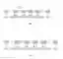
FIG. 1 is a structural diagram of a display panel according to a first embodiment of the present disclosure;
FIG. 2 is a structural diagram of a display panel according to a second embodiment of the present disclosure.
DETAILED DESCRIPTION OF PREFERRED EMBODIMENTS
Referring to FIG. 1, a display panel 100 according to a first embodiment of the disclosure includes a color filter plate substrate 10 and an array substrate 30, the color filter plate substrate 10 is formed on one side of a base substrate, the color filter plate substrate 10 and the array substrate 30 are disposed opposite. The display panel 100 is a liquid crystal display panel.
Similarly, the color filter plate substrate 10 includes light resistors 11, a black matrix 13 and a protective layer 15.The light resistors 11 includes at least resistors of three colors, in the embodiment, the resistance includes resistors of three colors, respectively are a red light resistor 111, a green light resistor 112, a blue light resistor 113. The red light resistor 111, the green light resistor 112, the blue light resistor 113 need to be formed on a corresponding region respectively, and the red light resistor 111, the green light resistor 112, the blue light resistor 113 are disposed alternately, therefore, a gap 115 is formed between two adjacent resistors 11.
Black matrixes 13 are formed alternately in the gap 115, therefore, the black matrixes 13 are disposed between two adjacent resistors 11.
Similarly, the black matrixes 13 can partially overlapped regions with contact areas of the red light resistor 111, the green light resistor 112, and the blue light resistor 113 along directions of the color filter plate substrate 10 respectively.
A protective layer 15 is disposed on a side of the black matrix 13 oriented to the array substrate 30 in a laser incidence region during laser repair., therefore, during repair process of the display panel 100, the laser is incident along a path from the array substrate 30 oriented to the color filter plate substrate 10, when intensity of the laser is excessive, the laser impacts on the protective layer 15 directly, which can prevent light leakage of the black matrixes 13 due to a through-hole defined by the powerful laser.
The protective layer 15 is an organic material layer.
The protective layer 15 is formed by a plurality of alternate spacer disposed on the black matrix 13. Similarly, a height of the plurality of spacer is the same, which can support the color filter plate substrate 10 and the array substrate 30 and ensure an equal distance between the color filter plate substrate 10 and the array substrate 30.
The array substrate 30 includes a thin film transistor (TFT) 31 and a metal wire 33, the spacer is disposed on a black matrix 13 of a position corresponding to the TFT 31 and metal wire 33.
The spacer is also disposed on a black matrix 13 of a position corresponding to a peripheral region of the array substrate 30, a contact area of the spacer corresponding to the TFT 31 and metal wire 33, and the black matrixes 13 is larger than a contact area of the spacer corresponding to the peripheral region of the array substrate 30 and the black matrixes 13. Therefore, a contact area of the spacer and the black matrixes 13 is enlarged merely in a laser radiation region, which can protect the black matrixes 13 from leakage formation due to the laser, as well as consuming less materials of the protective layer 15.
In the embodiment, distribution of the each spacer corresponding to the TFT 31 and metal wire 33 is more compact than that of the each spacer corresponding to the peripheral region of the array substrate 30.
Distinguishing from a conventional technique, the protective layer 15 is disposed on a side of the black matrix 13 oriented to the array substrate 30 in a laser incidence region during laser repair according to the disclosure, therefore, during repair process of the display panel 100, the preventive layer 15 can protect the black matrixes 13 during laser repair from forming a through-hole on the black matrix that can leak light. Meanwhile, distribution density of the spacer only in the laser radiation region is reduced to increase contact area of the spacer and the black matrixes 13, the black matrixes 13 can be protected from leakage due to laser and materials of the protective layer 15 are less consumed.
Referring to FIG. 2, difference of a display panel 200 according to a second embodiment of the disclosure and that according to the first embodiment is: a contact area of each spacer corresponding to a TFT 61 and a metal wire 63, and black matrixes 53 is larger than a contact area of the each spacer corresponding to the peripheral region of array substrate 60 and the black matrixes 53.
Distinguishing from a conventional technique, a protective layer 75 is disposed on a side of the black matrix 53 oriented to the array substrate 60 in a laser incidence region during laser repair according to the disclosure, therefore, during repair process of the display panel 200, the preventive layer 75 can protect the black matrixes 53 during laser repair from forming a through-hole on the black matrix 53 that can leak light. Meanwhile, distribution density of the spacer only in the laser radiation region is reduced to increase contact area of the spacer and the black matrixes 53, the black matrixes 53 can be protected from leakage due to laser and materials of the protective layer 75 are less consumed.
Above are embodiments of the present invention, which does not limit the scope of the present invention. Any modifications, equivalent replacements or improvements within the spirit and principles of the embodiment described above should be covered by the protected scope of the invention.
Claims
1. A display panel, wherein the display panel comprises:
a color filter plate substrate and an array substrate;
the color filter plate substrate comprises a black matrix and a protective layer;
the color filter plate substrate and the array substrate are disposed opposite;
the protective layer is disposed on a side of the black matrix oriented to the array substrate in a repairing laser incidence region.
2. The display panel according to claim 1, wherein the protective layer is an organic material layer.
3. The display panel according to claim 1, wherein the protective layer is formed by a plurality of alternate disposed on the black matrix layer.
4. The display panel according to claim 3, wherein the array substrate comprises a thin film transistor (TFT) and a metal wire, the spacer is disposed on the black matrix of a position corresponding to the TFT and metal wire.
5. The display panel according to claim 4, wherein the spacer is disposed between the black matrix and the array substrate, and a contact area of the spacer and the black matrix which corresponding to the position of the TFT and the metal wire are larger than a contact area of the spacer and the black matrix which corresponding to the position of the array substrate exposure area.
6. The display panel according to claim 5, wherein distribution of the each spacer corresponding to the TFT and metal wire is more compact than that of the each spacer corresponding to the peripheral region of the array substrate.
7. The display panel according to claim 5, wherein a contact area of the spacer corresponding to the TFT and metal wire, and the black matrix is larger than a contact area of the spacer corresponding to the peripheral region of the array substrate and the black matrix.
Images & Drawings included:

Sources:
- United States Patent and Trademark Office - verify current appl. status at the USPTO↗
Similar patent applications:
- » 20070258023
Dual-panel display panel, flat-panel display employing a dual-panel display panel, and method of showing images after the flat-panel display is turned off - » 20120300141
Lens panel, method for manufacturing the lens panel, display apparatus having the lens panel, display panel, a method for manufacturing the display panel and a display apparatus having the display panel - » 10446825
Display panel assembly, display panel case, display panel module, projection display device, and cooling method for the display panel module - » 20090225103
Driving device for display panel, display panel, display device including the driving device, and method for driving display panel - » 20230116030
Method of reducing color breakup of reflection of ambient light in display panel, display panel, display apparatus, and method of fabricating display panel - » 20110147751
DISPLAY PANEL SUBSTRATE, DISPLAY PANEL, METHOD FOR MANUFACTURING DISPLAY PANEL SUBSTRATE, AND METHOD FOR MANUFACTURING DISPLAY PANEL - » 20070126339
Method of manufacturing anode panel for flat-panel display device, method of manufacturing flat-panel display device, anode panel for flat-panel display device, and flat-panel display device - » 20080081533
METHOD OF MANUFACTURING ANODE PANEL FOR FLAT-PANEL DISPLAY DEVICE, METHOD OF MANUFACTURING FLAT-PANEL DISPLAY DEVICE, ANODE PANEL FOR FLAT-PANEL DISPLAY DEVICE, AND FLAT-PANEL DISPLAY DEVICE - » 20170084244
DISPLAY PANEL DRIVING APPARATUS, A METHOD OF DRIVING A DISPLAY PANEL USING THE DISPLAY PANEL DRIVING APPARATUS AND A DISPLAY APPARATUS HAVING THE DISPLAY PANEL DRIVING APPARATUS - » 20170186395
Display panel driving apparatus, a method of driving a display panel using the display panel driving apparatus and a display apparatus including the display panel driving apparatus
Recent applications in this class:
- » 20250284158 2025-09-11
OPTICAL SYSTEM - » 20250284157 2025-09-11
OPTICAL PATH CONTROL MEMBER AND DISPLAY DEVICE COMPRISING SAME - » 20250264752 2025-08-21
DISPLAY DEVICE AND ELECTRONIC APPARATUS - » 20250258404 2025-08-14
DISPLAY DEVICE - » 20250237903 2025-07-24
LIQUID CRYSTAL DISPLAY DEVICE - » 20250208463 2025-06-26
OPTICAL LAMINATE AND SUNROOF INCLUDING THE SAME - » 20250208462 2025-06-26
OPTICAL LAMINATE AND SUNROOF INCLUDING THE SAME - » 20250208461 2025-06-26
OPTICAL LAMINATE AND SUNROOF INCLUDING THE SAME - » 20250208460 2025-06-26
DISPLAY DEVICE - » 20250155746 2025-05-15
ELECTRONIC DEVICE
Recent applications for this Assignee:
- » 20250292712 2025-09-18
DISPLAY APPARATUS AND ELECTRONIC DEVICE - » 20250264763 2025-08-21
BACKLIGHT MODULE INCLUDING ANGULAR DEFLECTION FILM AND DISPLAY DEVICE INCLUDING THE SAME - » 20250252896 2025-08-07
PIXEL DRIVING CIRCUIT AND DISPLAY PANEL - » 20250248193 2025-07-31
DISPALY PANEL AND DISPLAY MODULE - » 20250244850 2025-07-31
TOUCH DISPLAY DEVICES AND TOUCH METHODS THEREOF - » 20250244577 2025-07-31
DISPLAY MODULE AND FIELD-OF-VIEW DISPLAY DEVICE FOR VEHICLE - » 20250225913 2025-07-10
LIGHT BOARDS AND DISPLAY PANELS - » 20250221126 2025-07-03
DISPLAY BACKPLANE AND DISPLAY DEVICE - » 20250218352 2025-07-03
Display Panel - » 20250212512 2025-06-26
DISPLAY PANEL