Pixels
US20170125465A1
2017-05-04
14/931,569
2015-11-03
✅ Patent granted
US 10,529,753 B2
2020-01-07
-
-
Dzung Tran
Locke Lord LLP | Scott D. Wofsy | Alicia J. Carroll
2035-11-03
Abstract:
A photodiode has an absorption layer and a cap layer operatively connected to the absorption layer. A pixel is formed in the cap layer and extends into the absorption layer to receive charge generated from photons therefrom. The pixel defines an annular diffused area to reduce dark current and capacitance. A photodetector includes the photodiode. The photodiode includes includes an array of pixels formed in the cap layer. At least one of the pixels extends into the absorption layer to receive charge generated from photons therefrom. At least one of the pixels defines an annular diffused area to reduce dark current and capacitance.
Inventors:
- Prabhu Mushini 3 🇺🇸 Annandale, NJ, United States
- Wei Huang 2 🇺🇸 Plainsboro, NJ, United States
Assignee:
- Sensors Unlimited, Inc. 131 🇺🇸 Princeton, NJ, United States
Applicant:
Interested in similar patents?
Get notified when new applications in this technology area are published.
Classification:
H01L27/14605 » CPC main
Devices consisting of a plurality of semiconductor or other solid-state components formed in or on a common substrate including semiconductor components sensitive to infra-red radiation, light, electromagnetic radiation of shorter wavelength or corpuscular radiation and specially adapted either for the conversion of the energy of such radiation into electrical energy or for the control of electrical energy by such radiation; Devices controlled by radiation; Imager structures; Structural or functional details thereof; Special geometry or disposition of pixel-elements, address-lines or gate-electrodes Structural or functional details relating to the position of the pixel elements, e.g. smaller pixel elements in the center of the imager compared to pixel elements at the periphery
H01L31/102 » CPC further
Semiconductor devices sensitive to infra-red radiation, light, electromagnetic radiation of shorter wavelength or corpuscular radiation and specially adapted either for the conversion of the energy of such radiation into electrical energy or for the control of electrical energy by such radiation; Processes or apparatus specially adapted for the manufacture or treatment thereof or of parts thereof; Details thereof in which radiation controls flow of current through the device, e.g. photoresistors characterised by at least one potential-jump barrier or surface barrier, e.g. phototransistors; Devices sensitive to infra-red, visible or ultra-violet radiation characterised by only one potential barrier or surface barrier
H01L27/14649 » CPC further
Devices consisting of a plurality of semiconductor or other solid-state components formed in or on a common substrate including semiconductor components sensitive to infra-red radiation, light, electromagnetic radiation of shorter wavelength or corpuscular radiation and specially adapted either for the conversion of the energy of such radiation into electrical energy or for the control of electrical energy by such radiation; Devices controlled by radiation; Imager structures; Photodiode arrays; MOS imagers Infra-red imagers
H01L27/146 IPC
Devices consisting of a plurality of semiconductor or other solid-state components formed in or on a common substrate including semiconductor components sensitive to infra-red radiation, light, electromagnetic radiation of shorter wavelength or corpuscular radiation and specially adapted either for the conversion of the energy of such radiation into electrical energy or for the control of electrical energy by such radiation; Devices controlled by radiation Imager structures
H01L31/0216 IPC
Semiconductor devices sensitive to infra-red radiation, light, electromagnetic radiation of shorter wavelength or corpuscular radiation and specially adapted either for the conversion of the energy of such radiation into electrical energy or for the control of electrical energy by such radiation; Processes or apparatus specially adapted for the manufacture or treatment thereof or of parts thereof; Details thereof; Details Coatings
H01L31/02161 » CPC further
Semiconductor devices sensitive to infra-red radiation, light, electromagnetic radiation of shorter wavelength or corpuscular radiation and specially adapted either for the conversion of the energy of such radiation into electrical energy or for the control of electrical energy by such radiation; Processes or apparatus specially adapted for the manufacture or treatment thereof or of parts thereof; Details thereof; Details; Coatings for devices characterised by at least one potential jump barrier or surface barrier
H01L31/03529 » CPC further
Semiconductor devices sensitive to infra-red radiation, light, electromagnetic radiation of shorter wavelength or corpuscular radiation and specially adapted either for the conversion of the energy of such radiation into electrical energy or for the control of electrical energy by such radiation; Processes or apparatus specially adapted for the manufacture or treatment thereof or of parts thereof; Details thereof characterised by their semiconductor bodies characterised by their shape or by the shapes, relative sizes or disposition of the semiconductor regions characterised by at least one potential jump barrier or surface barrier Shape of the potential jump barrier or surface barrier
H01L31/1035 » CPC further
Semiconductor devices sensitive to infra-red radiation, light, electromagnetic radiation of shorter wavelength or corpuscular radiation and specially adapted either for the conversion of the energy of such radiation into electrical energy or for the control of electrical energy by such radiation; Processes or apparatus specially adapted for the manufacture or treatment thereof or of parts thereof; Details thereof in which radiation controls flow of current through the device, e.g. photoresistors characterised by at least one potential-jump barrier or surface barrier, e.g. phototransistors; Devices sensitive to infra-red, visible or ultra-violet radiation characterised by only one potential barrier or surface barrier the potential barrier being of the PN homojunction type the devices comprising active layers formed only by AB compounds
H01L31/0352 IPC
Semiconductor devices sensitive to infra-red radiation, light, electromagnetic radiation of shorter wavelength or corpuscular radiation and specially adapted either for the conversion of the energy of such radiation into electrical energy or for the control of electrical energy by such radiation; Processes or apparatus specially adapted for the manufacture or treatment thereof or of parts thereof; Details thereof characterised by their semiconductor bodies characterised by their shape or by the shapes, relative sizes or disposition of the semiconductor regions
H01L31/103 IPC
Semiconductor devices sensitive to infra-red radiation, light, electromagnetic radiation of shorter wavelength or corpuscular radiation and specially adapted either for the conversion of the energy of such radiation into electrical energy or for the control of electrical energy by such radiation; Processes or apparatus specially adapted for the manufacture or treatment thereof or of parts thereof; Details thereof in which radiation controls flow of current through the device, e.g. photoresistors characterised by at least one potential-jump barrier or surface barrier, e.g. phototransistors; Devices sensitive to infra-red, visible or ultra-violet radiation characterised by only one potential barrier or surface barrier the potential barrier being of the PN homojunction type
H01L31/0224 IPC
Semiconductor devices sensitive to infra-red radiation, light, electromagnetic radiation of shorter wavelength or corpuscular radiation and specially adapted either for the conversion of the energy of such radiation into electrical energy or for the control of electrical energy by such radiation; Processes or apparatus specially adapted for the manufacture or treatment thereof or of parts thereof; Details thereof; Details Electrodes
H01L31/022416 » CPC further
Semiconductor devices sensitive to infra-red radiation, light, electromagnetic radiation of shorter wavelength or corpuscular radiation and specially adapted either for the conversion of the energy of such radiation into electrical energy or for the control of electrical energy by such radiation; Processes or apparatus specially adapted for the manufacture or treatment thereof or of parts thereof; Details thereof; Details; Electrodes for devices characterised by at least one potential jump barrier or surface barrier comprising ring electrodes
Description
BACKGROUND OF THE INVENTION
1. Field of the Invention
The present disclosure relates to photodiode arrays (PDAs), and more particularly to a unit pixel construction for photodiode arrays.
2. Description of Related Art
Traditional pixels made up of diodes (PN, PiN, Avalanche diodes, etc.), such as those used in photodiode arrays, contribute to the dark current and capacitance of the overall PDA. Pixel dark current and capacitance are key factors in determining the pixel performance. Lower values tend to indicate better pixel performance which ultimately translates to better signal to noise ratios at the overall camera and system levels. Pixel dark current and capacitance are significant contributors to the overall camera level noise. The unit pixel design plays a significant role in defining these contributing parameters to system level noise.
Such conventional pixel designs have generally been considered satisfactory for their intended purpose. However, there is still a need in the art for improved designs.
SUMMARY OF THE DISCLOSURE
A photodiode has an absorption layer and a cap layer operatively connected to the absorption layer. A pixel is formed in the cap layer and extends into the absorption layer to receive charge generated from photons therefrom. The pixel has an annular diffused area to reduce dark current and capacitance.
In accordance with some embodiments, the pixel includes a p-type material. The pixel can be generated through diffusion, implantation, epitaxial growth or the like. The absorption layer can be a semiconductor material able to detect optical signals from a light source through wavelengths ranging from the ultraviolet region to the long-wave infrared region. The cap layer can be a nominally doped semiconductor layer. The cap layer can be matched to the absorption layer and can have a wider bandgap material lattice than the absorption layer to provide passivation of the absorption layer.
The annular diffused area can define an inner diameter and an outer diameter. A portion of the cap layer can be within the inner diameter of the annular diffused area and a portion of the cap layer can be outside of the outer diameter of the annular diffused area. The absorption layer can be an indium gallium arsenide (InGaAs) absorption layer. The cap layer can be an indium phosphate (InP) cap layer. The photodiode can include a dielectric material layer overlaid on the cap layer opposite from the absorption layer. The dielectric material layer can cover the portion of the cap layer within the inner diameter of the annular diffused area.
In another aspect, a photodetector includes the photodiode as described above. The photodiode includes an absorption layer and a cap layer and operatively connected to the absorption layer. An array of pixels is formed in the cap layer. At least one of the pixels extends into the absorption layer to receive charge generated from photons therefrom. At least one of the pixels has an annular diffused area to reduce dark current and capacitance. In accordance with some embodiments, the photodetector includes a read-out integrated circuit (ROIC) operatively connected to the photodiode. The photodiode can include the dielectric material layer, described above, overlaid on the cap layer opposite from the absorption layer, between the cap layer and the ROIC.
These and other features of the systems and methods of the subject disclosure will become more readily apparent to those skilled in the art from the following detailed description of the preferred embodiments taken in conjunction with the drawings.
BRIEF DESCRIPTION OF THE DRAWINGS
So that those skilled in the art to which the subject disclosure appertains will readily understand how to make and use the devices and methods of the subject disclosure without undue experimentation, preferred embodiments thereof will be described in detail herein below with reference to certain figures, wherein:
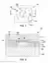
FIG. 1 is a schematic depiction of a top view of an exemplary embodiment of a portion of a photodiode constructed in accordance with the present disclosure, showing the pixel formed in the cap layer having an annular diffused area; and
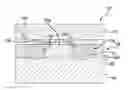
FIG. 2 is schematic depiction of a cross-sectional view of a photodetector constructed in accordance with the present disclosure, showing the ROIC operatively connected to the photodiode to form the photodetector.
DETAILED DESCRIPTION OF THE PREFERRED EMBODIMENTS
Reference will now be made to the drawings wherein like reference numerals identify similar structural features or aspects of the subject disclosure. For purposes of explanation and illustration, and not limitation, a top view of an exemplary embodiment of a photodiode in accordance with the disclosure is shown in FIG. 1 and is designated generally by reference character 100. Other embodiments of photodiodes in accordance with the disclosure, or aspects thereof, are provided in FIG. 2, as will be described. The photodiodes described have reduced dark current and capacitance as compared with traditional photodiodes, resulting in lower noise characteristics.
As shown in FIG. 1, a photodiode 100 has a cap layer 102. A pixel 106 is formed in cap layer 102 through one of diffusion, implantation, epitaxial growth, or the like. Pixel 106 has an annular diffused area 108 to reduce dark current and capacitance as compared to traditional pixels. It is contemplated that pixel 106 can be made from an acceptor material, e.g. zinc, or the like. Annular diffused area 108 defines an inner diameter 113 and an outer diameter 117. A portion 103a of cap layer 102 is within inner diameter 113 of annular diffused area 108 and a portion 103b of cap layer 102 is outside of outer diameter 117 of annular diffused area 108.
With reference now to FIG. 2, a photodetector 101 includes photodiode 100. Photodetector 101 includes a ROIC 116 operatively connected to a top metal layer 119 of photodiode 100 through bump bonding. Photodiode 100 includes an absorption layer 104 operatively connected to cap layer 102. Absorption layer 104 has specific absorption characteristics that allow it to absorb photons and generate electron hole pairs in that layer. Those skilled in the art will readily appreciate that absorption layer 104 is typically epitaxially grown on a highly doped substrate (not shown). It is contemplated that absorption layer 104 can be lattice matched to the substrate and in cases is also strained with stress with respect to the substrate.
With continued reference to FIG. 2, cap layer 102, a semiconductor layer usually of the same or larger bandgap material as absorption layer, is epitaxially grown on top of absorption layer 104. Cap layer 102 resists and/or prevents the exposure of absorption layer 104 to the natural elements and from oxidation or change to its semiconductor characteristics. It is contemplated that absorption layer 104 can be a semiconductor material able to detect optical signals from a light source through wavelengths ranging from the ultraviolet region to the long-wave infrared region, e.g. from 0.1-10 microns. Those skilled in the art will readily appreciate that cap layer 102 can be a nominally doped semiconductor layer. Cap layer 102 is matched to absorption layer 104 and has a wider bandgap material lattice than absorption layer 104 to provide passivation of absorption layer 104.
As shown in FIGS. 1 and 2, photodiode 100 includes a dielectric material layer 118 overlaid on cap layer 102 opposite from absorption layer 104. Dielectric material layer 118 covers portion 103a of cap layer 102 within inner diameter 113 of annular diffused area 108. Dielectric material layer 118 provides isolation for metal layer 119 from directly making contact with the undoped region of the semiconductor (e.g. portions 103a and 103b of cap layer 102). Metal layer 119 on top of pixel 106 only contacts the doped regions, e.g. annular diffused area 108, of pixel 106 to provide optimal ohmic contact and the subsequent diode characteristics such reverse leakage and capacitance. Those skilled in the art will readily appreciate that absorption layer 104 can have metal or semiconductor layers on top, bottom or both, e.g. cap layer 102, to form collection regions where the generated electron hole pairs are collected under bias to generate charge which is then collected by ROIC 116. Those skilled in the art will readily appreciate that absorption layer 104 can be an InGaAs absorption layer 104, or any other suitable semiconductor which can detect optical signals. It is also contemplated that cap layer 102 can be an InP cap layer 102, or the like.
Typically, collection regions in a photodiode that form the pixels (they can be anode or cathode) are fabricated by diffusing, implanting or epitaxially growing dopants to form P+0 or N+ regions on either side of an absorption layer through a cap layer. These P+ or N+ regions determine area and size of a pixel. In embodiments of the present disclosure, pixel 106 is formed by diffusing an acceptor or dopant species into the absorption layer through cap layer 102. Pixel 106 extends through cap layer 102 into absorption layer 104 to receive photons therefrom. Pixel 106 has an annular cylindrically shaped diffusion area 115 that extends into cap layer 102. Pixel 106 is defined by the area between the annular rings that includes the dopant species, e.g. between inner diameter 113 and outer diameter 117. The area of pixel 106 thus defined has lower area and volume of dopant species that traditional pixels, which leads to a smaller depletion region than a traditional pixel generally defined by a fully enclosed circular area. The lower depletion region created by the annular pixel design of pixel 106 yields lower dark current and capacitance both of which are also dependent on the pixel area.
The annular shape of pixel 106 reduces diffused area 108 as compared with traditional pixels thereby reducing the overall diffused, implanted or epitaxially grown charge to form the junction diode, thereby reducing the depletion region of the diode without reducing the absorption capability of pixel 106. This leads to lower dark current and capacitance, reducing noise and improving the signal to noise ratio in the camera in which photodiode 100 is being used.
The methods and systems of the present disclosure, as described above and shown in the drawings, provide for discharge systems having superior properties including the ability to reduce dark current and capacitance, without reducing absorption capabilities of the pixel. While the apparatus and methods of the subject disclosure have been shown and described with reference to embodiments, those skilled in the art will readily appreciate that changes and/or modifications may be made thereto without departing from the spirit and scope of the subject disclosure.
Claims
What is claimed is:1. A photodiode comprising:
an absorption layer;
a cap layer operatively connected to the absorption layer; and
a pixel formed in the cap layer and extending into the absorption layer to receive charge generated from photons therefrom, wherein the pixel defines an annular diffused area.
2. The photodiode as recited in claim 1, wherein the pixel includes a p-type material.
3. The photodiode as recited in claim 1, wherein the pixel is generated through at least one of diffusion, implantation or epitaxial growth.
4. The photodiode as recited in claim 1, wherein the absorption layer is a semiconductor material able to detect optical signals from a light source through wavelengths ranging from the ultraviolet region to the long-wave infrared region.
5. The photodiode as recited in claim 1, wherein the cap layer is a nominally doped semiconductor layer, wherein the cap layer is matched to the absorption layer, and wherein the cap layer has a wider bandgap material lattice than the absorption layer to provide passivation of the absorption layer.
6. The photodiode as recited in claim 1, wherein the annular diffused area defines an inner diameter and an outer diameter, wherein a portion of the cap layer is within the inner diameter of the annular diffused area and a portion of the cap layer is outside of the outer diameter of the annular diffused area.
7. The photodiode as recited in claim 6, wherein the photodiode includes a dielectric material layer overlaid on the cap layer opposite from the absorption layer, wherein the dielectric material layer covers the portion of the cap layer within the inner diameter of the annular diffused area.
8. A photodetector comprising:
a photodiode, wherein the photodiode includes:
an absorption layer;
a cap layer operatively connected to the absorption layer; and
an array of pixels formed in the cap layer, wherein at least one of the pixels extends into the absorption layer to receive charge generated from photons therefrom, wherein at least one of the pixels has an annular diffused area.
9. The photodetector as recited in claim 8, wherein at least one of the pixels includes a p-type material.
10. The photodetector as recited in claim 8, wherein the pixels are generated through at least one of diffusion, implantation or epitaxial growth.
11. The photodetector as recited in claim 8, wherein the absorption layer is a semiconductor material able to detect optical signals from a light source through wavelenghths ranging from ultraviolet region to long-wave infrared region.
12. The photodetector as recited in claim 8, wherein the cap layer is a nominally doped semiconductor layer, wherein the cap layer is matched to the absorption layer, and wherein the cap layer has a wider bandgap material lattice than the absorption layer to provide passivation of the absorption layer.
13. The photodetector as recited in claim 8, further comprising a read-out integrated circuit (ROIC) operatively connected to the photodiode.
14. The photodetector as recited in claim 8, wherein the annular diffused area defines an inner diameter and an outer diameter, wherein a portion of the cap layer is within the inner diameter of the annular diffused area and a portion of the cap layer is outside of the outer diameter of the annular diffused area.
15. The photodetector as recited in claim 14, further comprising a read-out integrated circuit (ROIC) operatively connected to the photodiode, wherein the photodiode includes a dielectric material layer overlaid on the cap layer opposite from the absorption layer, between the cap layer and the ROIC, wherein the dielectric material layer covers the portion of the cap layer within the inner diameter of the annular diffused area.
Images & Drawings included:
Sources:
- United States Patent and Trademark Office - verify current appl. status at the USPTO↗
Similar patent applications:
- » 20210382360
Pixel structure comprising two red sub-pixels having equal areas, two green sub-pixels having equal areas, and a blue sub-pixel having a greater area than the two green sub-pixels and a smaller area than the two red sub-pixels - » 20090225371
Image forming apparatus and method calculating a deviation between a) a representative point of threshold information I) nearest to the coordinate of a pixel of interest or II) in dither space nearest to the address coordinate of the pixel of interest in dither space, and b) the address coordinate in dither space corresponding to a pixel coordinate of an integer in pixel space or a pixel coordinate of an integer in pixel space nearest to the representative point - » 20170316291
Information processing apparatus for setting an attribute of a pixel based on a conformity between pixel values of objects, information processing method for setting an attribute of a pixel based on a conformity between pixel values of objects, and non-transitory computer readable medium for setting an attribute of a pixel based on a conformity between pixel values of objects - » 20230007198
Solid-state imaging device and electronic apparatus with a charge storage unit electrically connected to each of a lower electrode of a phase difference detection pixel, an adjacent pixel and a normal pixel via a capacitance, wherein the capacitance connected to the adjacent pixel is greater than a capacitance connected to the normal pixel - » 20210003893
Reflective LCD panel by disposing a white sub-pixel unit in the pixel unit and using the while sub-pixel unit in collaboration with the pixel electrode to increase brightness of the pixel unit - » 20060028233
Pixel testing method, method of correcting output voltage of pixel, defect pixel processing device, defect pixel processing program, defect pixel processing method, and recording medium having program - » 20100128202
Pixel structure having red sub-pixel, green sub-pixel, blue sub-pixel and white sub-pixel - » 20160366357
Image sensing device comprising dummy pixel row and active pixel rows coupled to read-out column line, and using a high speed active pixel row read-out method that reduces settling time by precharging the column line during a dummy pixel row selection time between active pixel row selection times - » 20200006445
Display device including a first pixel, a second pixel and a third pixel at least partially separated from each of the first pixel and the second pixel - » 20080013632
Integer pixel motion estimation system, motion estimation system for quarter-pixel luminance, motion estimation system for quarter-pixel chrominance, motion estimation system for combined luminance, motion estimation system for combined luminance and chrominance, and motion estimation system for quarter-pixel luminance and chrominance
Recent applications in this class:
- » 20250056905 2025-02-13
PHOTONIC STRUCTURE AND METHODS OF MANUFACTURING - » 20250040271 2025-01-30
IMAGE SENSOR AND IMAGE CAPTURE APPARATUS - » 20250040270 2025-01-30
IMAGE SENSOR WITH SHARED EXTRINSIC REGION - » 20250040269 2025-01-30
PHOTODETECTION DEVICE AND DISTANCE MEASURING SYSTEM - » 20250015101 2025-01-09
COLOR ROUTER BASED PHOTODIODES AND INTEGRATED PIXEL CIRCUIT - » 20250006750 2025-01-02
PHOTOELECTRIC CONVERSION APPARATUS, MANUFACTURING METHOD, AND EQUIPMENT - » 20250006749 2025-01-02
IMAGE SENSING COMPUTING UNIT AND ITS OPERATING METHOD, IMAGE SENSING COMPUTER AND ELECTRONIC DEVICE - » 20240429252 2024-12-26
IMAGE SENSOR AND METHOD OF FABRICATING THE SAME - » 20240413177 2024-12-12
IMAGE SENSOR AND METHOD OF FABRICATING THE SAME - » 20240387569 2024-11-21
MULTISPECTRAL SENSOR AND ELECTRONIC DEVICE
Recent applications for this Assignee:
- » 20240292074 2024-08-29
Neuromorphic compressive sensing in low-light environment - » 20240036176 2024-02-01
DETECTION PIXELS AND PIXEL SYSTEMS - » 20230333221 2023-10-19
TIME-OF-FLIGHT DISTANCE COMPENSATION THRESHOLD RAMP DRIVER - » 20230307481 2023-09-28
PHOTODETECTOR ARRAY (PDA) METALLIZATION - » 20230307398 2023-09-28
Hybridization bumps for fine pitch sensor arrays - » 20230305259 2023-09-28
SYSTEMS AND METHODS FOR ALIGNING IMAGING DEVICES - » 20230299223 2023-09-21
PHOTODIODE STRUCTURES - » 20230050990 2023-02-16
Visible-swir hyper spectral photodetectors with reduced dark current - » 20220079447 2022-03-17
VISUALIZATION FOR FLUORESCENT GUIDED IMAGING - » 20210288100 2021-09-16
Low capacitance photo detectors