High power and high frequency plastic pre-molded cavity package
US20170170102A1
2017-06-15
14/966,636
2015-12-11
✅ Patent granted
US 9,865,528 B2
2018-01-09
-
-
Kimberly Rizkallah | Dilinh Nguyen
Perry + Currier Inc.
2035-12-11
Abstract:
A cavity package is set forth along with a method of manufacturing thereof. According to one embodiment, the method comprises attaching a metal heat sink to a leadframe using an intermediate structure that is thermally conductive and electrically insulating; molding a plastic body around the heat sink and exposed leads of the leadframe to form a cavity, with partially and selectively exposed lead top surfaces, heat sink top surface, and heat sink bottom surface; attaching a semiconductor device die within cavity on to the exposed top surface of the heat sink using a thermal conductive material; wire bonding respective wire bond pads of the semiconductor device die to the exposed lead top surfaces and to the heat sink for grounding; and attaching a lid to the plastic molded body to protect the wire bonded device within cavity.
Assignee:
- UBOTIC COMPANY LIMITED 2 🇭🇰 Tsuen Wan, Hong Kong
Applicant:
Interested in similar patents?
Get notified when new applications in this technology area are published.
Classification:
H01L23/293 » CPC further
Details of semiconductor or other solid state devices; Encapsulations, e.g. encapsulating layers, coatings, e.g. for protection characterised by the material, e.g. carbon Organic, e.g. plastic
H01L21/563 » CPC further
Processes or apparatus adapted for the manufacture or treatment of semiconductor or solid state devices or of parts thereof; Manufacture or treatment of semiconductor devices or of parts thereof the devices having at least one potential-jump barrier or surface barrier, e.g. PN junction, depletion layer or carrier concentration layer; Assembly of semiconductor devices using processes or apparatus not provided for in a single one of the subgroups - , e.g. sealing of a cap to a base of a container; Encapsulations, e.g. encapsulation layers, coatings Encapsulation of active face of flip-chip device, e.g. underfilling or underencapsulation of flip-chip, encapsulation preform on chip or mounting substrate
H01L24/43 » CPC further
Arrangements for connecting or disconnecting semiconductor or solid-state bodies; Methods or apparatus related thereto; Means for bonding being attached to, or being formed on, the surface to be connected, e.g. chip-to-package, die-attach, "first-level" interconnects; Manufacturing methods related thereto; Wire connectors; Manufacturing methods related thereto Manufacturing methods
H01L24/46 » CPC further
Arrangements for connecting or disconnecting semiconductor or solid-state bodies; Methods or apparatus related thereto; Means for bonding being attached to, or being formed on, the surface to be connected, e.g. chip-to-package, die-attach, "first-level" interconnects; Manufacturing methods related thereto; Wire connectors; Manufacturing methods related thereto; Structure, shape, material or disposition of the wire connectors prior to the connecting process of a plurality of wire connectors
H01L23/29 IPC
Details of semiconductor or other solid state devices; Encapsulations, e.g. encapsulating layers, coatings, e.g. for protection characterised by the material, e.g. carbon
H01L21/52 » CPC further
Processes or apparatus adapted for the manufacture or treatment of semiconductor or solid state devices or of parts thereof; Manufacture or treatment of semiconductor devices or of parts thereof the devices having at least one potential-jump barrier or surface barrier, e.g. PN junction, depletion layer or carrier concentration layer; Assembly of semiconductor devices using processes or apparatus not provided for in a single one of the subgroups - , e.g. sealing of a cap to a base of a container Mounting semiconductor bodies in containers
H01L21/56 IPC
Processes or apparatus adapted for the manufacture or treatment of semiconductor or solid state devices or of parts thereof; Manufacture or treatment of semiconductor devices or of parts thereof the devices having at least one potential-jump barrier or surface barrier, e.g. PN junction, depletion layer or carrier concentration layer; Assembly of semiconductor devices using processes or apparatus not provided for in a single one of the subgroups - , e.g. sealing of a cap to a base of a container Encapsulations, e.g. encapsulation layers, coatings
H01L23/49568 » CPC main
Details of semiconductor or other solid state devices; Arrangements for conducting electric current to or from the solid state body in operation, e.g. leads, terminal arrangements ; Selection of materials therefor consisting of soldered constructions; Lead-frames or other flat leads specifically adapted to facilitate heat dissipation
H01L23/00 IPC
Details of semiconductor or other solid state devices
H01L23/3675 » CPC further
Details of semiconductor or other solid state devices; Arrangements for cooling, heating, ventilating or temperature compensation ; Temperature sensing arrangements; Selection of materials, or shaping, to facilitate cooling or heating, e.g. heatsinks; Cooling facilitated by shape of device characterised by the shape of the housing
H01L23/495 IPC
Details of semiconductor or other solid state devices; Arrangements for conducting electric current to or from the solid state body in operation, e.g. leads, terminal arrangements ; Selection of materials therefor consisting of soldered constructions Lead-frames or other flat leads
H01L23/3731 » CPC further
Details of semiconductor or other solid state devices; Arrangements for cooling, heating, ventilating or temperature compensation ; Temperature sensing arrangements; Selection of materials, or shaping, to facilitate cooling or heating, e.g. heatsinks; Cooling facilitated by selection of materials for the device or materials for thermal expansion adaptation, e.g. carbon Ceramic materials or glass
H01L24/06 » CPC further
Arrangements for connecting or disconnecting semiconductor or solid-state bodies; Methods or apparatus related thereto; Means for bonding being attached to, or being formed on, the surface to be connected, e.g. chip-to-package, die-attach, "first-level" interconnects; Manufacturing methods related thereto; Bonding areas ; Manufacturing methods related thereto; Structure, shape, material or disposition of the bonding areas prior to the connecting process of a plurality of bonding areas
H01L24/32 » CPC further
Arrangements for connecting or disconnecting semiconductor or solid-state bodies; Methods or apparatus related thereto; Means for bonding being attached to, or being formed on, the surface to be connected, e.g. chip-to-package, die-attach, "first-level" interconnects; Manufacturing methods related thereto; Layer connectors, e.g. plate connectors, solder or adhesive layers; Manufacturing methods related thereto; Structure, shape, material or disposition of the layer connectors after the connecting process of an individual layer connector
H01L24/48 » CPC further
Arrangements for connecting or disconnecting semiconductor or solid-state bodies; Methods or apparatus related thereto; Means for bonding being attached to, or being formed on, the surface to be connected, e.g. chip-to-package, die-attach, "first-level" interconnects; Manufacturing methods related thereto; Wire connectors; Manufacturing methods related thereto; Structure, shape, material or disposition of the wire connectors after the connecting process of an individual wire connector
H01L24/49 » CPC further
Arrangements for connecting or disconnecting semiconductor or solid-state bodies; Methods or apparatus related thereto; Means for bonding being attached to, or being formed on, the surface to be connected, e.g. chip-to-package, die-attach, "first-level" interconnects; Manufacturing methods related thereto; Wire connectors; Manufacturing methods related thereto; Structure, shape, material or disposition of the wire connectors after the connecting process of a plurality of wire connectors
H01L24/73 » CPC further
Arrangements for connecting or disconnecting semiconductor or solid-state bodies; Methods or apparatus related thereto Means for bonding being of different types provided for in two or more of groups , , , , , , ,
H01L24/92 » CPC further
Arrangements for connecting or disconnecting semiconductor or solid-state bodies; Methods or apparatus related thereto; Methods for connecting semiconductor or solid state bodies including different methods provided for in two or more of groups - Specific sequence of method steps
H01L24/97 » CPC further
Arrangements for connecting or disconnecting semiconductor or solid-state bodies; Methods or apparatus related thereto; Batch processes at chip-level, i.e. with connecting carried out on a plurality of singulated devices, i.e. on diced chips the devices being connected to a common substrate, e.g. interposer, said common substrate being separable into individual assemblies after connecting
H01L2224/04042 » CPC further
Indexing scheme for arrangements for connecting or disconnecting semiconductor or solid-state bodies and methods related thereto as covered by; Means for bonding being attached to, or being formed on, the surface to be connected, e.g. chip-to-package, die-attach, "first-level" interconnects; Manufacturing methods related thereto; Bonding areas; Manufacturing methods related thereto; Structure, shape, material or disposition of the bonding areas prior to the connecting process Bonding areas specifically adapted for wire connectors, e.g. wirebond pads
H01L2224/73265 » CPC further
Indexing scheme for arrangements for connecting or disconnecting semiconductor or solid-state bodies and methods related thereto as covered by; Means for bonding being of different types provided for in two or more of groups; Location after the connecting process on different surfaces Layer and wire connectors
H01L2224/92247 » CPC further
Indexing scheme for arrangements for connecting or disconnecting semiconductor or solid-state bodies and methods related thereto as covered by; Methods for connecting semiconductor or solid state bodies including different methods provided for in two or more of groups - ; Specific sequence of method steps; Connecting different surfaces of the semiconductor or solid-state body with connectors of different types; Sequential connecting processes the first connecting process involving a layer connector the second connecting process involving a wire connector
H01L2224/97 » CPC further
Indexing scheme for arrangements for connecting or disconnecting semiconductor or solid-state bodies and methods related thereto as covered by; Batch processes at chip-level, i.e. with connecting carried out on a plurality of singulated devices, i.e. on diced chips the devices being connected to a common substrate, e.g. interposer, said common substrate being separable into individual assemblies after connecting
H01L2924/16195 » CPC further
Indexing scheme for arrangements or methods for connecting or disconnecting semiconductor or solid-state bodies as covered by; Details of package parts other than the semiconductor or other solid state devices to be connected; Cap; Shape Flat cap [not enclosing an internal cavity]
H01L21/44 IPC
Processes or apparatus adapted for the manufacture or treatment of semiconductor or solid state devices or of parts thereof; Manufacture or treatment of semiconductor devices or of parts thereof the devices having at least one potential-jump barrier or surface barrier, e.g. PN junction, depletion layer or carrier concentration layer the devices having semiconductor bodies not provided for in groups, , , and with or without impurities, e.g. doping materials Manufacture of electrodes on semiconductor bodies using processes or apparatus not provided for in groups -
H01L21/48 IPC
Processes or apparatus adapted for the manufacture or treatment of semiconductor or solid state devices or of parts thereof; Manufacture or treatment of semiconductor devices or of parts thereof the devices having at least one potential-jump barrier or surface barrier, e.g. PN junction, depletion layer or carrier concentration layer Manufacture or treatment of parts, e.g. containers, prior to assembly of the devices, using processes not provided for in a single one of the subgroups -
H01L21/50 » CPC further
Processes or apparatus adapted for the manufacture or treatment of semiconductor or solid state devices or of parts thereof; Manufacture or treatment of semiconductor devices or of parts thereof the devices having at least one potential-jump barrier or surface barrier, e.g. PN junction, depletion layer or carrier concentration layer Assembly of semiconductor devices using processes or apparatus not provided for in a single one of the subgroups - , e.g. sealing of a cap to a base of a container
H01L23/373 IPC
Details of semiconductor or other solid state devices; Arrangements for cooling, heating, ventilating or temperature compensation ; Temperature sensing arrangements; Selection of materials, or shaping, to facilitate cooling or heating, e.g. heatsinks Cooling facilitated by selection of materials for the device or materials for thermal expansion adaptation, e.g. carbon
H01L23/367 IPC
Details of semiconductor or other solid state devices; Arrangements for cooling, heating, ventilating or temperature compensation ; Temperature sensing arrangements; Selection of materials, or shaping, to facilitate cooling or heating, e.g. heatsinks Cooling facilitated by shape of device
H01L23/04 » CPC further
Details of semiconductor or other solid state devices; Containers; Seals characterised by the shape of the container or parts, e.g. caps, walls
H01L23/49548 » CPC further
Details of semiconductor or other solid state devices; Arrangements for conducting electric current to or from the solid state body in operation, e.g. leads, terminal arrangements ; Selection of materials therefor consisting of soldered constructions; Lead-frames or other flat leads; Geometry of the lead-frame Cross section geometry
H01L24/29 » CPC further
Arrangements for connecting or disconnecting semiconductor or solid-state bodies; Methods or apparatus related thereto; Means for bonding being attached to, or being formed on, the surface to be connected, e.g. chip-to-package, die-attach, "first-level" interconnects; Manufacturing methods related thereto; Layer connectors, e.g. plate connectors, solder or adhesive layers; Manufacturing methods related thereto; Structure, shape, material or disposition of the layer connectors prior to the connecting process of an individual layer connector
Description
FIELD OF INVENTION
The present invention relates generally to integrated circuits, and more particularly in one aspect to a high power, high frequency plastic pre-molded cavity package and in another aspect to a hermetically sealed high power, high frequency plastic pre-molded cavity package.
BACKGROUND
Ceramic cavity and plastic over-mold with embedded heat sink packages are known in the art for housing high power, high frequency devices such as RF power transistors. Cermaic cavity packages are designed with a cavity (containing air or nitrogen) for housing a semiconductor die (IC), whereas plastic-molded packages contain minimal air in the package. The basic structure of such packages is a die attach pad on which the semiconductor die is mounted, a thermally conductive heat sink or heat spreader for dissipating heat from the die, metal leads for signal input/output with the semiconductor die, and a cap or lid. In cavity packages, the lid is metal whereas in over-mold plastic packages the entire package is over-molded in plastic, but with a portion of the heat sink exposed.
Prior art ceramic cavity packages are expensive in terms of the material used, exhibit poor thermal performance due to the use of ceramic-copper-based laminate material for the heat sink, and are not scalable for mass production.
One reason for the development of plastic over-molded with embedded heat sink packages was to provide improved thermal performance over ceramic cavity packages. Plastic packages use a copper heat sink on which the IC is mounted instead of the copper-based laminate material used in prior art cavity packages, such that when the die is mounted on the copper heat spreader, there is a reduction in the thermal resistance as compared to when the die is mounted on air cavity packages having a ceramic-copper-based laminate heat sink.
Also, prior art ceramic cavity packages are typically assembled individually, whereas plastic packages are assembled in a leadframe configuration as a group. This makes the assembly process faster and results in less manual handling.
However, plastic over-mold with embedded heat sink packages suffer from the disadvantage of not providing a cavity, as well as lacking a good thermal path from the leadframe to the heat sink because the top surface of the heat sink does not in direct contact with the bottom surface of the leads of the leadframe.
SUMMARY
A cavity package and method of fabrication are set forth for ameliorating at least some of the disadvantages of prior art ceramic and plastic over-mold packages. According to a first embodiment of the present invention, a metal heat sink is attached to a leadframe via an intermediate structure that is thermally conductive but electrically insulating. A plastic body is molded onto the integrated heat sink and leadframe to form a cavity, with partially and selectively exposed lead surfaces as well as top and bottom surfaces of the heat sink. The die is attached to the exposed top surface of the heat sink within the cavity and wire bonded to the lead surfaces. Finally, a lid is attached to the plastic molded body to seal the cavity.
In accordance with another aspect of the first embodiment, there is provided a method comprising attaching a metal heat sink to a leadframe using an intermediate structure that is thermally conductive and electrically insulating; molding a plastic body around the heat sink and exposed leads of the leadframe to form a cavity, with partially and selectively exposed lead top surfaces, heat sink top surface, and heat sink bottom surface; attaching a semiconductor device die within cavity on to the exposed top surface of the heat sink using a thermal conductive material; wire bonding respective wire bond pads of the semiconductor device die to the exposed lead top surfaces and to the heat sink for grounding; and attaching a lid to the plastic molded body to protect the wire bonded device within cavity.
According to a second embodiment, a metal heat sink is attached to a leadframe via a first intermediate ring-type structure that is thermally conductive but electrically insulating. A further thermally conductive and electrically insulating ring-type intermediate structure is attached to the top of the leadframe. In one embodiment, each ring-type structure preferably comprises a “sandwich” of thin metal portions bonded to top and bottom surfaces of a ceramic middle portion. Opposite sides of the top thin metal portion of the first ring-type structure are bonded to respective bottom surfaces of the metal leads, while the bottom surface of the first ring-type structure is bonded to the heat sink. Opposite sides of the bottom thin metal portion of the further ring-type structure are bonded to respective top surfaces of the metal leads. A plastic body is molded onto the integrated heat sink and leadframe to form a cavity, with partially and selectively exposed portions of the metal leads as well as top and bottom surfaces of the heat sink and the top thin metal portion of the further ring-type intermediate structure. The die is attached to the exposed top surface of the heat sink within the cavity and wire bonded to the lead surfaces. Finally, a metal lid is attached to the plastic molded body to seal the cavity.
In accordance with a further aspect of the second embodiment, there is provided a method comprising attaching a metal heat sink to a leadframe using an intermediate structure that is thermally conductive and electrically insulating; molding a plastic body around the heat sink and exposed leads of the leadframe to form a cavity, with partially and selectively exposed lead top surfaces, heat sink top surface, and heat sink bottom surface; attaching a semiconductor device die within cavity on to the exposed top surface of the heat sink using a thermal conductive material; wire bonding respective wire bond pads of the semiconductor device die to the exposed lead top surfaces and to the heat sink for grounding; and attaching a metal lid to the plastic molded body to protect the wire bonded device within cavity.
In accordance with an additional aspect the metal heat sink comprises copper (Cu) or other metal alloy.
In a variant of the first embodiment, the intermediate structure is ceramic.
In accordance with an additional aspect, the leadframe preferably includes a rectangular outer frame.
In accordance with an additional aspect of the first embodiment, the thermal conductive material comprises one of either silver epoxy or solder.
In accordance with an additional aspect of the first embodiment, the lid is attached to the plastic molded body by means of epoxy.
In accordance with an additional aspect of the first embodiment, the lid is made of liquid crystal polymer, epoxy mold compound, metal or other suitable material.
In accordance with a further aspect of the first embodiment, a cavity package is provided comprising a plastic body surrounding and partially exposing an integrated heat sink and leads of a leadframe, and a lid.
In accordance with an additional aspect of the first embodiment, the cavity package includes a pair of leads extending from opposite sides of the leadframe.
In accordance with an additional aspect of the first embodiment, the cavity package includes at least two leads extending from each side of the leadframe.
According to a further aspect of the second embodiment, each intermediate “sandwich” structure comprises ceramic with Direct Bond Copper (DBC) in which a thin layer of copper is bonded to the top and bottom surfaces of the ceramic middle portion. The thin layers of copper are electrically isolated from each other by the intermediate ceramic portion. The shape of the ceramic portion as well as the pattern of the thin layers of copper can be designed and fabricated in accordance with methodologies known to persons of skill in the art. The bottom thin layer of copper of the first intermediate structure is bonded to the top side of the heat sink (e.g. using Ag epoxy or soldering). In one embodiment, the pattern of the bottom thin layer of copper is a complete ring pattern. Since the top thin layer of copper is designed to bond to the bottom side of the two leads of the package and since the two leads are eventually electrically isolated after singulation, the pattern of the top thin layer of copper of the first intermediate structure can be a broken ring shape (e.g. a “[ ]” shape, for a two-lead package design).
In accordance with an additional aspect of the second embodiment, the thermal conductive material of both the first and further intermediate structures comprises one of either silver epoxy or solder.
In accordance with an additional aspect of the second embodiment, the lid is attached to the metal ring portion of the further intermediate structure on top of the metal leads, for example via solder.
In accordance with an additional aspect of the second embodiment, the lid may be made of copper, stainless steel plated with nickel and/or Sn to facilitate the soldering process.
The cavity package according to the present invention is small and lightweight, with good thermal and electrical performance that makes it suitable for industrial high power and high frequency applications. The cavity package according to the present invention is more cost effective than ceramic cavity packages because it uses more common materials such as copper and plastic epoxy molding compound, and can be manufactured in high volume due to its multiple leadframe construction.
The cavity package according to the present invention is suitable for high frequency and high power applications (e.g. RF switching transistors) by providing an integrated heat sink for dissipating heat generated by the die and wires through the leadframe and intermediate structure. High frequency operation is made possible due to the air cavity in which the die and bonded wires are disposed (air having the best dielectric constant for high speed).
BRIEF DESCRIPTION OF THE DRAWINGS
Features and advantages of the invention will be apparent from the detailed description which follows, taken in conjunction with the accompanying drawings, which together illustrate, by way of example, features of the invention; and, wherein:
FIGS. 1A and 1B are top and bottom perspective views, respectively, of a cavity package according to an exemplary first embodiment.
FIG. 2 is a flow chart showing steps of a method for fabricating the cavity package of FIGS. 1A and 1B.
FIGS. 3A and 3B are top and bottom perspective views, respectively, showing attachment of a heat sink to the bottom of a leadframe, according to the method of FIG. 2.
FIGS. 4A and 4B are top perspective views taken from the side and end, respectively, showing the molding of a plastic body onto the integrated heat sink and leadframe of FIGS. 3A and 3B, for forming a cavity, according to the method of FIG. 2.
FIG. 4C is a bottom perspective view showing the molding of a plastic body onto the integrated heat sink and leadframe of FIGS. 3A and 3B, according to the method of FIG. 2.
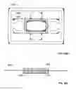
FIGS. 5A and 5B are top perspective and plan views, respectively, showing attachment of a semiconductor die (integrated circuit) onto an exposed portion of the heat sink within the cavity, according to the method of FIG. 2.
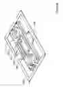
FIGS. 6A and 6B are top perspective detail and full views, respectively, showing wire bonding of the die to exposed lead top surfaces, according to the method of FIG. 2.
FIGS. 7A and 7B are plan and top perspective views, respectively, showing attachment of a lid for covering and sealing the cavity, according to the method of FIG. 2.
FIGS. 8A and 8B are top and bottom perspective views, respectively, of a cavity package according to a second exemplary embodiment.
FIG. 9 is a flow chart showing steps of a method for fabricating the cavity package of FIGS. 8A and 8B.
FIGS. 10A and 10B are top and bottom perspective views, respectively, showing attachment of a heat sink to the bottom of a leadframe via a thermally conductive and electrically insulating ring-type intermediate structure, according to the method of FIG. 9.
FIGS. 10C, 10D and 10E are top perspective, plan and elevation views, respectively, showing attachment of a further thermally conductive and electrically insulating ring-type intermediate structure to the top of the leadframe, according to the method of FIG. 9.
FIGS. 11A and 11B are top and bottom perspective views, respectively, showing the molding of a plastic body onto the integrated heat sink and leadframe of FIGS. 10A and 10B, for forming a cavity, according to the method of FIG. 9.
FIGS. 12A and 12B are top perspective and plan views, respectively, showing attachment of a semiconductor die (integrated circuit) onto an exposed portion of the heat sink within the cavity, according to the method of FIG. 9.
FIGS. 13A and 13B are top perspective detail and full views, respectively, showing wire bonding of the die to exposed lead top surfaces, according to the method of FIG. 9.
FIGS. 14A and 14B are plan and top perspective views, respectively, showing attachment of a metal lid for covering and sealing the cavity, according to the method of FIG. 9.
FIG. 15 is a flow chart showing steps of an alternative method for fabricating the cavity package of FIGS. 1A and 1B.
FIG. 16 is a top perspective view of a leadframe for the cavity package of FIGS. 1A and 1B.
FIG. 17 is a top perspective view showing a pair of leads of the leadframe each bent downwardly to form a step, according to the alternative method for fabricating the cavity package of FIG. 15.
FIG. 18 is a top perspective view showing attachment of a heat sink to the bottom of the leadframe, according to the alternative method of FIG. 15.
Reference will now be made to the exemplary embodiments illustrated, and specific language will be used herein to describe the same. It will nevertheless be understood that no limitation of the scope of the invention is thereby intended.
DETAILED DESCRIPTION OF EXAMPLE EMBODIMENTS
Before the present invention is disclosed and described, it is to be understood that this invention is not limited to the particular structures, process steps, or materials disclosed herein, but is extended to equivalents thereof as would be recognized by those ordinarily skilled in the relevant arts. It should also be understood that terminology employed herein is used for the purpose of describing particular embodiments only and is not intended to be limiting.
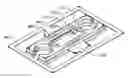
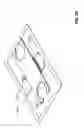
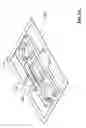
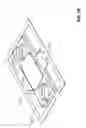
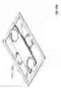
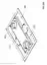
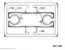
A high power, high frequency plastic pre-molded cavity package 100 is shown in FIGS. 1A and 1B, according to a first exemplary embodiment, comprising a plastic body 110 surrounding and partially exposing an integrated heat sink 120 and leads 130 of a leadframe 300 (see FIGS. 3A and 3B), and a lid 140.
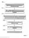
With reference to FIGS. 3A through 7B, construction of cavity package 100 is shown, according to steps of an exemplary method depicted in FIG. 2. It should be noted that whereas FIGS. 3A through 7B set forth construction of a single cavity package, in practice a matrix comprising a plurality of cavity packages is fabricated so that multiple packages are fabricated simultaneously and then singulated into individual packages.
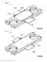
Construction of the cavity package begins at step 200 (FIG. 2) with attachment a metal heat sink (e.g. Cu or other metal alloy) to leadframe 300 using an intermediate structure 310 that is thermally conductive and electrically insulating. In one variant, the intermediate structure 310 is ceramic. As illustrated in FIGS. 3A and 3B, the leadframe 300 preferably includes a rectangular outer frame that forms one of a plurality of repeating units (not shown) to form a matrix for simultaneously fabrication a post-manufacturing singulation, as discussed above. Also, although only a pair of leads 130 are shown extending from opposite sides of the leadframe, it is contemplated that two or more leads may extend from each side, depending on the intended application of the cavity package.
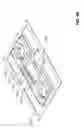
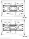
At step 210, plastic body 110 is molded around the integrated heat sink 120 and leads 130 of leadframe 300 to form a cavity 400, with partially and selectively exposed lead top surface 410, heat sink top surface 420, and heat sink bottom surface 430, as shown in FIGS. 4A-4C. The exposed heat sink bottom surface 430 conducts heat from the cavity 400 to be dissipated in a mother board (not shown) to which the cavity package is mounted post-fabrication.
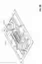
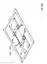
At step 220, a semiconductor device die 500 (i.e. the IC) is placed within cavity 400 on to exposed top surface 420 of the heat sink and attached to the using a thermal conductive material, such as silver epoxy, solder, etc., as shown in FIGS. 5A and 5B.
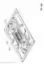
Respective wire bond pads of semiconductor device die 500 are then wire bonded 600 to the exposed lead top surfaces 410 and to the heat sink 120 for grounding, at step 230, as shown in FIGS. 6A and 6B. For example, when used in a high power, high frequency application such as a RF switching transistor, one lead is bonded to the transistor source and the other lead is bonded to the transistor drain, wherein the drain of the transistor chip comprises the entire die back side such that once the die 500 is attached to the heat sink 120, the heat sink becomes the drain. The die top has a source pad as well as the gate pad such that one of the leads can be connected to the source while the other lead is connected to the gate.
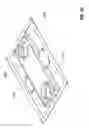
Finally, at step 240, lid 140 is attached 11190 is attached to the plastic molded body 110 by means of epoxy to protect the wire bonded device within cavity 400. The lid may be made of liquid crystal polymer, epoxy mold compound, metal or other suitable material.
As discussed above, in practice a matrix of cavity packages is fabricated (not shown) such that after the lid 140 has been attached, the matrix is singulated (e.g. using saw singulation) to create packages, such as the package shown in FIGS. 1A and 1B.
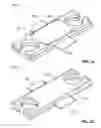
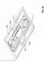
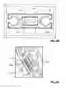
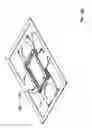
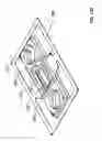
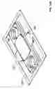
A high power, high frequency plastic pre-molded cavity package 100 is shown in FIGS. 8A and 8B, according to a second exemplary embodiment, comprising a plastic body 110′ surrounding and partially exposing an integrated heat sink 120′ and leads 130′ of a leadframe 300′ (see FIGS. 10A and 10B), and a lid 140′.
With reference to FIGS. 10A through 14B, construction of cavity package 100 is shown, according to steps of an exemplary method depicted in FIG. 9. It should be noted that whereas FIGS. 10A through 14B set forth construction of a single cavity package, in practice a matrix comprising a plurality of cavity packages is fabricated so that multiple packages are fabricated simultaneously and then singulated into individual packages.
Construction of the cavity package begins at step 200′ (FIG. 9) with attachment metal heat sink 120′ (e.g. Cu or other metal alloy) to leadframe 300′ using a first ring-type intermediate structure 310′ that is thermally conductive and electrically insulating. In one embodiment, the intermediate structure 310′ comprises a “sandwich” structure of ceramic and Direct Bond Copper (DBC), wherein a thin layer of copper is bonded to top and bottom surfaces of a ceramic middle portion. The shape of the ceramic portion as well as the pattern of the thin layers of copper can be designed and fabricated in accordance with methodologies known to persons of skill in the art. The bottom thin layer of copper of the first intermediate structure is bonded to the top side of the heat sink (e.g. using Ag epoxy or soldering). In one embodiment, the pattern of the bottom thin layer of copper is a complete ring pattern. Since the top thin layer of copper is designed to bond to the bottom side of the two leads of the package and since the two leads are eventually electrically isolated after singulation, the pattern of the top thin layer of copper of the first intermediate structure can be a broken ring shape (e.g. a “[ ]” shape, for a two-lead package design), as shown in FIG. 10A.
As illustrated in FIGS. 10A and 10B, the leadframe 300′ preferably includes a rectangular outer frame that forms one of a plurality of repeating units (not shown) to form a matrix for simultaneously fabrication a post-manufacturing singulation, as discussed above. Also, although only a pair of leads 130′ are shown extending from opposite sides of the leadframe, it is contemplated that two or more leads may extend from each side, depending on the intended application of the cavity package.
A further thermally conductive and electrically insulating intermediate ring-type structure 320′ is then attached (step 205′) to the top surface of leads 130′ of leadframe 300′. The further intermediate structure 320′ is of similar “sandwich” construction as the first structure 310′. The bottom thin layer of copper is attached to the metal leads 310′ such that the pattern can be either a broken ring (i.e. “[ ]”) or a parallel line pair, whereas the top thin layer of the copper forms a complete ring pattern onto which a lid is attached (see FIGS. 14A and 14B).
At step 210′, plastic body 110′ is molded around the integrated heat sink 120′ and leads 130′ of leadframe 300′ to form a cavity 400′, with partially and selectively exposed lead top surface 410′, heat sink top surface 420′, heat sink bottom surface 430′, and top surface of ring-type structure 320′, as shown in FIGS. 11-11C. The exposed heat sink bottom surface 430′ conducts heat from the cavity 400′ to be dissipated in a mother board (not shown) to which the cavity package is mounted post-fabrication.
At step 220′, a semiconductor device die 500′ (i.e. the IC) is placed within cavity 400′ on to exposed top surface 420′ of the heat sink and attached to the using a thermal conductive material, such as silver epoxy, solder, etc., as shown in FIGS. 12A and 12B.
Respective wire bond pads of semiconductor device die 500′ are then wire bonded 600′ to the exposed lead top surfaces 410′ and to the heat sink 120′ for grounding, at step 230′, as shown in FIGS. 13A and 13B. For example, when used in a high power, high frequency application such as a RF switching transistor, one lead is bonded to the transistor source, the other lead is bonded to the transistor gate, with the entire die back side acting as the drain such that once the die is attached to the heat sink 120′, the heat sink becomes the drain. The top of the die 500′ has both a source pad as well as the gate pad wire bonded respectively to the two leads 130′.
Finally, at step 240′, metal lid 140′ is attached to the plastic molded body 110′ by means of soldering to the top exposed ring on the further (i.e. top) intermediate structure 320′. The metal lid 140′ is stronger than a plastic lid, is cheaper than ceramic, and can be fabricated from a one of many metals such as copper or stainless steel with plated nickel or tin.
As discussed above, in practice a matrix of cavity packages is fabricated (not shown) such that after the lid 140′ has been attached, the matrix is singulated (e.g. using saw singulation) to create packages, such as the package shown in FIGS. 8A and 8B.
FIG. 15 is a flow chart showing steps of an alternative method for fabricating the cavity package of FIGS. 1A and 1B, where steps 210-240 are identical to the method of FIG. 2. The alternative method of claim 15 is a lower cost alternative to the method of FIG. 2 because it eliminates the need for intermediate structure 310.
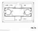
At step 195, a leadframe 300, as depicted in FIG. 16, is prepared for attaching the heatsink 120 thereto, by bending lead tips 160 downwardly by a predetermined amount to form a step, as shown in FIG. 17.
At step 198, the metal heat sink 120 (e.g. Cu or other metal alloy) is attached to the bottom of the leadframe 300 using an electrically insulative interface (e.g. non-conductive epoxy, double sided adhesive tape, etc. . . . )
Following the heat sink attachment step 198, the remaining molding, die attach, wire bonding and lid attachment steps 210-240 are performed, as discussed above with reference to FIG. 2.
The many features and advantages of the invention are apparent from the detailed specification and, thus, it is intended by the appended claims to cover all such features and advantages of the invention that fall within the true spirit and scope of the invention. Further, since numerous modifications and changes will readily occur to those skilled in the art, it is not desired to limit the invention to the exact construction and operation illustrated and described, and accordingly all suitable modifications and equivalents may be resorted to, falling within the scope of the invention.
Claims
1.
2.
3. A method of manufacturing a cavity package comprising:
i) attaching a metal heat sink to a leadframe using a first intermediate ring-type structure that is thermally conductive and electrically insulating;
ii) attaching a further thermally conductive and electrically insulating ring-type intermediate structure to the top of the leadframe;
iii) molding a plastic body around the heat sink and exposed leads of the leadframe to form a cavity, with partially and selectively exposed metal leads, heat sink top surface, heat sink bottom surface, and top metallic portion of the further thermally conductive and electrically insulating ring-type intermediate structure;
iv) attaching a semiconductor device die within cavity on to the exposed top surface of the heat sink using a thermal conductive material;
v) wire bonding respective wire bond pads of the semiconductor device die to the exposed leads and to the heat sink for grounding; and
vi) attaching a metal lid to the plastic molded body by means of soldering to the exposed top metallic portion of the further ring-type intermediate structure to protect the wire bonded device within cavity.
4. A cavity package constructed in accordance with the method of claim 3, wherein each of the first and further ring-type structures comprises a sandwich of thin metal portions bonded to top and bottom surfaces of a ceramic middle portion.
5. The cavity package according to claim 4, wherein opposite sides of the top metallic portion of the first ring-type structure are bonded to respective bottom surfaces of the metal leads, and the bottom surface of the first ring-type structure is bonded to the heat sink.
6. The cavity package according to claim 5, wherein opposite sides of the bottom metallic portion of the further ring-type structure are bonded to respective top surfaces of the metal leads.
7.
Images & Drawings included:
Sources:
- United States Patent and Trademark Office - verify current appl. status at the USPTO↗
Similar patent applications:
Recent applications in this class:
- » 20250273545 2025-08-28
SEMICONDUCTOR DEVICE AND FABRICATING METHOD THEREOF - » 20250253212 2025-08-07
SEMICONDUCTOR PACKAGE HAVING AN ELECTRICAL CONTACT MEMBER FOR DOWN-CONNECTING A CONTACT PAD WITH A SUBSTRATE - » 20250246525 2025-07-31
DUAL COOLED MOSFET FOR LOW RDSON AND LOW THERMAL POWER - » 20250239506 2025-07-24
SEMICONDUCTOR MODULE - » 20250210477 2025-06-26
SEMICONDUCTOR PACKAGING STRUCTURE - » 20250201680 2025-06-19
INTELLIGENT POWER MODULE - » 20250192008 2025-06-12
SEMICONDUCTOR DEVICE AND A METHOD OF MANUFACTURING A SEMICONDUCTOR DEVICE - » 20250174529 2025-05-29
SEMICONDUCTOR DEVICE AND SEMICONDUCTOR PACKAGE INCLUDING THE SAME - » 20250174528 2025-05-29
Methods of packaging high voltage and high current power devices - » 20250157897 2025-05-15
SEMICONDUCTOR MODULE
Recent applications for this Assignee:
- » 20150060116 2015-03-05
Cavity package with pre-molded substrate