Method of improving adhesion
US20170178901A1
2017-06-22
15/383,162
2016-12-19
✅ Patent granted
US 10,096,468 B2
2018-10-09
-
-
Jasmine Clark
2037-01-23
Abstract:
A method is for improving adhesion between a semiconductor substrate and a dielectric layer. The method includes depositing a silicon dioxide adhesion layer onto the semiconductor substrate by a first plasma enhanced chemical vapor deposition (PECVD) process, and depositing the dielectric layer onto the adhesion layer by a second PECVD process. The first PECVD process is performed in a gaseous atmosphere comprising tetraethyl orthosilicate (TEOS) either in the absence of O2 or with O2 introduced into the process at a flow rate of 250 sccm or less.
Inventors:
- ANDREW PRICE 3 🇬🇧 GWENT, United Kingdom
- STEPHEN R. BURGESS 15 🇬🇧 GWENT, United Kingdom
- KATHRINE CROOK 2 🇬🇧 WOTTON-UNDER-EDGE, United Kingdom
Assignee:
- SPTS TECHNOLOGIES LIMITED 76 🇬🇧 NEWPORT, United Kingdom
Applicant:
Interested in similar patents?
Get notified when new applications in this technology area are published.
Classification:
H01L21/02304 » CPC main
Processes or apparatus adapted for the manufacture or treatment of semiconductor or solid state devices or of parts thereof; Manufacture or treatment of semiconductor devices or of parts thereof; Forming layers; Forming insulating materials on a substrate characterised by the treatment performed before or after the formation of the layer pre-treatment formation of intermediate layers, e.g. buffer layers, layers to improve adhesion, lattice match or diffusion barriers
H01L29/0649 » CPC further
Semiconductor devices adapted for rectifying, amplifying, oscillating or switching, or capacitors or resistors with at least one potential-jump barrier or surface barrier, e.g. PN junction depletion layer or carrier concentration layer; Details of semiconductor bodies or of electrodes thereof; Multistep manufacturing processes therefor; Semiconductor bodies ; Multistep manufacturing processes therefor characterised by their shape; characterised by the shapes, relative sizes, or dispositions of the semiconductor regions ; characterised by the concentration or distribution of impurities within semiconductor regions characterised by particular constructional design considerations, e.g. for preventing surface leakage, for controlling electric field concentration or for internal isolations regions; Isolation within the component, i.e. internal isolation Dielectric regions, e.g. SiO regions, air gaps
H01L21/02 IPC
Processes or apparatus adapted for the manufacture or treatment of semiconductor or solid state devices or of parts thereof Manufacture or treatment of semiconductor devices or of parts thereof
H01L29/06 IPC
Semiconductor devices adapted for rectifying, amplifying, oscillating or switching, or capacitors or resistors with at least one potential-jump barrier or surface barrier, e.g. PN junction depletion layer or carrier concentration layer; Details of semiconductor bodies or of electrodes thereof; Multistep manufacturing processes therefor; Semiconductor bodies ; Multistep manufacturing processes therefor characterised by their shape; characterised by the shapes, relative sizes, or dispositions of the semiconductor regions ; characterised by the concentration or distribution of impurities within semiconductor regions
Description
BACKGROUND
This invention relates to a method of improving adhesion between a semiconductor substrate and a dielectric layer. The method relates also to a structure comprising a semiconductor substrate, a dielectric layer and a silicon dioxide adhesion layer.
There are a great many processes, structures and devices of commercial significance which involve the deposition of a dielectric layer onto a surface of a semiconductor substrate. One example is the manufacture of CIS (CMOS Image Sensor) products. In these manufacturing processes, it is necessary to deposit a dielectric layer by plasma enhanced chemical vapour deposition (PECVD) for TSV (Through Silicon Via) isolation and interposer passivation in via reveal applications. Low temperature, high etch rate silicon etch processes produce a significant amount of unwanted polymeric by-product. This is particularly pronounced in TSV and Via Reveal Applications. The polymer by-product needs to be removed before any isolation layers are deposited. One reason for this is that the presence of polymeric by-product compromises the adhesion of subsequently deposited dielectric layers. Removal of the by-product requires multiple cleaning steps, including O2 ashing and an EKC polymer strip. These processes can themselves result in other residues remaining on the silicon surface. These residues can also result in poor adhesion of dielectric layers.
Typically, 300 mm silicon substrates are bonded to glass carrier substrates prior to thinning and etching of the silicon. The adhesive used for the bonding has unstable vacuum properties which necessitate that outgassing is carried out prior to CVD deposition. However, there is potential for the outgas by-products to contaminate the silicon surface. Contamination of the silicon surface by processes such as these is undesirable. One consequence of the contamination is that the adhesion of subsequently deposited dielectric layers is compromised. Therefore, it can be seen that it can be challenging to ensure adequate adhesion of dielectric layers to semiconductor structures as part of commercial fabrication processes.
SUMMARY
It will be appreciated that, in addition to the specific problems described above, there is a general desire and need to improve the adhesion of dielectric layers to semiconductor substrate such as silicon, whether or not the semiconductor surface is contaminated. The present invention, in at least some of its embodiments, addresses these problems, desires and needs.
According to a first aspect of the invention there is provided a method of improving adhesion between a semiconductor substrate and a dielectric layer comprising the steps of:
-
- depositing a silicon dioxide adhesion layer onto the semiconductor substrate by a first Plasma Enhanced Chemical Vapor Deposition (PECVD) process; and
- depositing the dielectric layer onto the adhesion layer by a second PECVD process;
- in which the first PECVD process is performed in a gaseous atmosphere comprising tetraethyl orthosilicate (TEOS) either in the absence of O2 or with O2 introduced into the process at a flow rate of 250 sccm or less.
O2 may be introduced into the process at a flow rate of 100 sccm or less, preferably 10 sccm or less. Most preferably, no O2 is introduced into the process.
The semiconductor substrate may be silicon.
The semiconductor substrate onto which the adhesion layer is deposited may comprise additional non-semiconductor features. The non-semiconductor features may be metal features. For example, the semiconductor substrate may be a partially metallised silicon substrate having copper or tungsten features thereon. Typically, the non-semiconductor features constitute only a small proportion of the available surface area. Generally, the non-semiconductor features constitute less than 10% of the available surface area of the semiconductor substrate.
The semiconductor substrate may comprise a contaminated surface onto which the adhesion layer is deposited.
The semiconductor substrate may comprise a surface onto which the adhesion layer is deposited, wherein the surface is hydrophobic.
The dielectric layer which is deposited onto the adhesion layer may be a silicon-containing material. The dielectric layer may be silicon nitride, a silicon oxide or a silicon carbide. Where the dielectric layer is a silicon oxide, this may be silicon dioxide deposited using a suitable precursor such as TEOS or silane.
The dielectric layer which is deposited onto the adhesion layer may be hydrophilic.
The first PECVD process may use an RF signal to produce a plasma. The RF signal may be of a frequency of less than 400 kHz. Typically, the RF signal is of a frequency of greater than 100 kHz. Particularly advantageous results have been obtained using a single RF signal at these frequencies to produce the plasma.
It is also possible to use dual RF signals to produce the plasma, with one of the RF signals being of a relatively low frequency and the other RF signal being of a relatively high frequency. The RF power can be applied to a showerhead or a showerhead and platen assembly. Thus, the first PECVD process may additionally use a second RF signal to produce the plasma. The second RF signal may be of a frequency of greater than 400 kHz. Preferably, the second RF signal is of a frequency of 13.56 MHz.
The first PECVD process may be performed in a gaseous atmosphere which comprises TEOS, optionally O2, and one or more further components.
The first PECVD process may be performed in a gaseous atmosphere which comprises H2. H2 may be introduced into the first PECVD process at a flow rate in the range 500 to 1200 sccm. The H2 flow rate may be in the range 800-1100 sccm.
The first PECVD process may be performed with TEOS introduced into the process at a flow rate of 1.3 to 1.6 ccm.
The silicon dioxide adhesion layer may have a thickness of 1000 nm or less, preferably 200 nm or less. Thicker adhesion layers are within the scope of the invention. However, in embodiments where the silicon dioxide adhesion layer is a poorer dielectric than the dielectric layer which is deposited onto it, it may be beneficial to utilize a relatively thin adhesion layer, such an adhesion layer having a thickness of 200 nm or less.
The adhesion layer may have a CHx:SiO ratio of at least 0.3%. The CHx:SiO ratio may be at least 3%. The CHx:SiO ratio as described herein is calculated by comparing peak areas obtained by Fourier Transform Infra-Red Spectroscopy (FTIR) which are associated with CHx and SiO absorptions. X may be 1 to 3. The CHx:SiO ratio may be the ratio of the intergrated area of the CHx peaks at about 2900-3000 cm−1 to the integrated area of the SiO peak at about 1800 cm−1, expressed as a percentage.
The first PECVD process may be performed at a pressure in the range 2.0 to 4.0 Torr. The pressure may be in the range 2.0 to 3.5 Torr. The pressure may be in the range 2.0 to 3.0 Torr.
The first PECVD process maybe performed at a temperature in the range 100 to 200° C.
According to a second aspect of the invention there is provided a semiconductor substrate, a dielectric layer and a silicon dioxide adhesion layer formed between the semiconductor substrate and the dielectric layer, the structure being manufactured by a method in accordance with the first aspect of the invention.
According to a third aspect to the invention there is provided a structure comprising a semiconductor substrate, a dielectric layer and a silicon dioxide adhesion layer formed between the semiconductor substrate and the dielectric layer, in which the adhesion layer has a CHx:SiO ratio of at least 0.3%, as calculated by comparing peak areas obtained by FTIR which are associated with CHx and SiO absorptions, wherein x is 1 to 3. The adhesion layer may have a CHx:SiO ratio of at least 3%.
Whilst the invention has been described above, it extends to any inventive combination of the features set out above or in the following description, drawings or claims.
BRIEF DESCRIPTION OF THE DRAWINGS
Embodiments of methods and structures in accordance with the invention will now be described with reference to the accompanying drawings, in which:
FIG. 1 shows I-V curves for three adhesion layers;
FIG. 2 shows I-V curves obtained directly after deposition and after five days;
FIG. 3 shows FTIR spectra of a silicon dioxide layer obtained using a conventional TEOS based PECVD process and using a TEOS based PECVD process with no O2 present; and
FIG. 4 is a schematic representation of a structure of the invention.
DETAILED DESCRIPTIONS OF EMBODIMENTS
FIG. 4 is a schematic representation of the structure 40 of the invention comprising a semiconductor substrate 42, an adhesion layer 44 and a dielectric layer 46. The invention utilises the adhesion layer 44 to improve adhesion between the semiconductor substrate 42 and the dielectric layer 46. The adhesion layer 44 is a silicon dioxide layer which is deposited onto the semiconductor substrate 42 in a PECVD process which utilises a low oxygen flow or no oxygen flow at all. The dielectric layer 46 is deposited onto the adhesion layer 44 by PECVD. Examples of the invention and comparative examples are presented below.
Semiconductor Substrate
In order to replicate a contaminated silicon surface, a low temperature (50-200° C.) in-situ polymer strip plasma was run directly onto bare silicon surfaces. Typical process conditions are shown in Table 1.
| TABLE 1 |
| Polymer strip process (HF = high frequency RF = |
| 13.56 MHz, LF = Low frequency RF = 380 kHz). |
| Process Parameter | Typical Values | |
| Time (sec) | 30 | |
| Temperature (° C.) | 125 | |
| Pressure (Torr) | 3.1 | |
| Gas flows (sccm) | 2300O2, 1000H2 | |
| RF Power (Watts) | 945 HF, 420 LF | |
The contaminated silicon surface is believed to representative of the contaminated surfaces which commonly occur on device wafers.
Numerous PECVD depositions were made onto the contaminated silicon surfaces. The adhesion of the deposited layers was quantified by using a standard tape pull test. In the pull test, a 10×10 1mm grid is diamond scribed through the film into the silicon substrate. Adhesive tape is applied to the surface of the film and pulled off perpendicularly to the silicon surface. A percentage adhesion pass is quoted which refers to how much of the film in the grid remains adhered to the silicon.
Adhesion Layer
Silicon dioxide adhesion layers were deposited in a TEOS PECVD process using little or no oxygen flow into the PECVD process. Table 2 shows typical ranges and preferred (although non-limiting) values for the PECVD process parameters. The low RF frequency utilised was 380 kHz and the high RF frequency utilised was 13.56 MHz. Other frequencies might instead be used. In general, a low RF frequency can be considered to be a frequency of less than 400 kHz, and a high RF frequency can be considered to be a frequency of 400 kHz or more.
| TABLE 2 |
| Process parameters for adhesion layer. |
| Parameter | Range | Preferred | |
| Temperature (° C.) | 100-200 | 125 | |
| Pressure (torr) | 2.5-4.0 | 3 | |
| Oxygen (sccm) | 0-500 | 0 | |
| Hydrogen (sccm) | 500-1200 | 1000 | |
| TEOS (ccm) | 1.35-1.55 | 1.45 | |
| Power (high frequency RF) | 0-600 | 0 | |
| (watts) | |||
| Power (low frequency RF) | 350-600 | 420 | |
| (watts) | |||
Adhesion tests were performed on silicon dioxide adhesion layers deposited under different conditions. The results are shown in Table 3.
| TABLE 3 |
| Adhesion tests of silicon dioxide adhesion layers |
| (low pressure = 2.5 Torr, other processes at pressure of 4.0 Torr). |
| Deposition Conditions | Adhesion Test Result | |
| Low frequency RF, 500 sccm | 90% pass | |
| oxygen flow | ||
| High frequency RF, no oxygen flow | 100% pass | |
| Low frequency RF, no oxygen flow | 100% pass | |
| Low frequency RF, no oxygen flow, | 100% pass | |
| lower pressure | ||
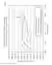
The films described in Table 3 which were deposited with no oxygen flow underwent further tests to investigate their electric characteristics. FIG. 1 shows I-V curves 10, 12, 14 for the high RF frequency, low RF frequency, and low RF frequency and low pressure embodiments, respectively. Table 4 shows leakage current and breakdown voltage.
| TABLE 4 |
| Leakage current at breakdown voltage for various films. |
| Leakage Current | ||
| @ 2 MV/cm | Breakdown Voltage | |
| (A/cm2) | (MV/cm) | |
| High Frequency | 1.09E−05 | >7 | |
| Low Frequency | 2.73E−07 | >8 | |
| Low Frequency and | 2.27E−09 | >9 | |
| Pressure | |||
It can be seen that the electrical current characteristics of the silicon dioxide films deposited using a low RF frequency are superior to those deposited using a high RF frequency. A reduction in the process pressure further improves the electrical characteristics. For a dielectric film, it is desirable to maximise the breakdown voltage and minimise the leakage current at a fixed potential such as 2 MV/cm.
Film stability was investigated by measuring electrical properties directly after deposition and after exposure of the film to ambient conditions for five days. FIG. 2 shows the associated I-V curves. Curves 20, 22 correspond to the low RF frequency deposition measured directly after deposition and after five days, respectively. Curves 24, 26 correspond to the low RF frequency and low pressure deposition measured directly after deposition and after five days, respectively. Table 5 shows leakage current measured directly after deposition and after five days. The films obtained using low RF frequency show only a marginal increase over five days. The films obtained using low RF frequency with low pressure deposition show no increase in leakage current, which indicates minimal reabsorption.
| TABLE 5 |
| Leakage current at breakdown voltage at deposition |
| and after five days. |
| Leakage Current @ 2 MV/cm | ||
| (A/cm2) |
| Deposition conditions | As Deposited | Day 5 | |
| Low Frequency RF | 2.73E−07 | 4.4E−07 | |
| Low Frequency RF and | 2.27E−09 | 1.64E−09 | |
| Pressure | |||
FTIR spectra were also obtained over this period. Table 6 shows normalised FTIR peak areas corresponding to the 3400 cm−1 and 950 cm−1 —OH absorptions. Again, the adhesion layer deposited using low RF frequency and low deposition pressure shows a lower moisture content than the other films. Regarding the films obtained with the higher process pressure conditions, the low RF frequency adhesion layer shows significantly lower moisture content than the high RF frequency adhesion layer.
| TABLE 6 |
| Normalised —OH peak area ratio from FTIR spectra |
| for various films. |
| Normalised —OH Peak Area |
| 3400 cm−1 | 950 cm−1 |
| As | As | |||
| Deposited | 5 Days | Deposited | 5 Days | |
| High Frequency | 0.126 | 0.190 | 0.003 | 0.007 |
| Low Frequency | 0.053 | 0.113 | −0.006 | −0.002 |
| Low | 0.045 | 0.092 | −0.005 | −0.002 |
| Frequency/Pressure | ||||
The carbon content of the silicon dioxide adhesion layers was measured and compared to silicon dioxide layers deposited using conventional TEOS PECVD processes. These results are shown in Table 7. It can be seen that the silicon dioxide adhesion layers of the invention have a higher CHx content than the conventionally obtained silicon dioxide films. The CHx content is expressed as the CHx:SiO ratio. This ratio is obtained by comparing peak areas in FTIR spectra corresponding to CHx and SiO absorptions.
FIG. 3 show FTIR Spectra of a silicon dioxide adhesion layer of the invention and a silicon dioxide layer deposited using a conventional TEOS
PECVD process. The large peak at ca.1080 cm−1 is the SiO stretching absorption. The peaks at ca. 2900-3000 cm−1 are associated with CHx absorptions. The CHx:SiO peak area ratios presented below are obtained by calculating the ratio of the integrated area of the 2900-3000 cm−1 peaks to the integrated area of the 1080 cm−1 peak.
The CHx groups render the silicon dioxide adhesion layer slightly hydrophobic. This is compatible with the hydrophobic contaminated surface of the silicon substrate. It is noted that silicon dioxide layers deposited using silane based PECVD have no carbon bonding and are also hydrophilic in nature.
| TABLE 7 |
| CHx:SiO ratios for TEOS based SiO2 depositions. |
| CHx:SiO | ||
| Film | Peak Area Ratio (%) | |
| TEOS Oxide standard | 0 | |
| TEOS 500 sccm O2 | 0.379 | |
| TEOS No O2 | 4.068 | |
Deposition of Dielectric Layer
A range of dielectric films were deposited including silicon nitrides and silicon dioxide films deposited by TEOS based PECVD and silane based PECVD. Films were deposited at thicknesses ranging from 500 nm to 3 microns and temperatures from 50-400° C. Films were deposited either directly onto the contaminated silicon surface, or onto a silicon dioxide adhesion layer. Representative deposition conditions are shown in Table 8.
| TABLE 8 |
| Deposition conditions use for sample preparation |
| (HF = High frequency RF = 13.56 MHz, LF = Low frequency |
| RF = 380 kHz). |
| O/N | |||||
| reactant | |||||
| Temp | Pressure | flow | RF Power | ||
| Process | (° C.) | (Torr) | Si reactant flow | (sccm) | (Watts) |
| TEOS | 125 | 3.1 | 1.45ccm TEOS | 2300 O2 | 945 HF/ |
| Based SiO2 | 420 LF | ||||
| Silane | 300 | 2.15 | 175 sccm SiH4 | 3000 N2O | 550 HF |
| based SiO2 | |||||
| Si3N4 | 265 | 0.7 | 125 sccm | 245 NH3/ | 57 HF |
| SiH4 | 1800 N2 | ||||
Properties of Deposited Dielectric Layers
Adhesion tests were performed with dielectric films deposited directly onto the contaminated silicon surface. Experiments were also performed depositing a 100 nm silicon dioxide adhesion layer onto the silicon surface and subsequently depositing the dielectric layer onto the adhesion layer by PECVD. The adhesion layer was deposited using the low RF frequency, low pressure PECVD process described above. The thicknesses of the deposited dielectric layers were 3 microns, 600 nm and 500 nm for the TEOS based silicon dioxide, silane based silicon dioxide, and silicon nitride films, respectively. The results of the adhesion tests shown in Table 9.
| TABLE 9 |
| Adhesion tests on dielectric layers deposited onto |
| contaminated silicon surface with and without an |
| intermediate adhesion layer. |
| Adhesion Test | ||
| Dielectric | Results | |
| Comparative | Silicon dioxide (TEOS based | 0% | |
| Example 1 | PECVD) | ||
| Comparative | Silicon dioxide (silane based | 10% pass | |
| Example 2 | PECVD) | ||
| Comparative | Silicon nitride | 5% pass | |
| Example 3 | |||
| Example 1 | Silicon dioxide (TEOS based | 100% pass | |
| PECVD)/ | |||
| Silicon dioxide adhesion | |||
| layer | |||
| Example 2 | Silicon dioxide (silane based | 100% pass | |
| PECVD)/ | |||
| silicon dioxide adhesion layer | |||
| Example 3 | Silicon nitride/silicon dioxide | 100% pass | |
| adhesion layer | |||
Without wishing to be limited by any particular theory or conjecture, the silicon dioxide adhesion layer is thought to act as a bonding layer between the hydrophobic surface of the contaminated silicon and the slightly hydrophilic dielectric layers. Again without wishing to be limited by any particular theory or conjecture, it is believed that with the low or no oxygen flow utilised in the invention to produce the silicon dioxide adhesion layer, the process substantially or even wholly relies on oxygen liberated from TEOS to form the silicon dioxide layer.
The invention can be used to deposit a wide range of dielectric layers onto the adhesion layer by PECVD. It is particularly convenient when the deposited dielectric layer is also silicon dioxide. The strength of the bond is then maximised by allowing the ‘seed’ deposition of the adhesion layer to proceed into the main silicon dioxide dielectric layer without interrupting deposition. This results in a continuous transition between films, promoting excellent adhesion of the composite layer.
Claims
What is claimed is:1. A method of improving adhesion between a semiconductor substrate and a dielectric layer comprising the steps of:
depositing a silicon dioxide adhesion layer onto the semiconductor substrate by a first plasma enhanced chemical vapor deposition (PECVD) process; and
depositing the dielectric layer onto the adhesion layer by a second PECVD process;
in which the first PECVD process is performed in a gaseous atmosphere comprising tetraethyl orthosilicate (TEOS) either in the absence of O2 or with O2 introduced into the process at a flow rate of 250 sccm or less.
2. A method according to claim 1 in which O2 is introduced into the process at a flow rate of 100 sccm or less.
3. A method according to claim 2 in which O2 is introduced into the process at a flow rate of 10 sccm or less.
4. A method according to claim 1 in which the semiconductor substrate is silicon.
5. A method according to claim 1 in which the dielectric layer is a silicon-containing material.
6. A method according to claim 5 in which the dielectric layer is silicon nitride, silicon oxide or silicon carbide.
7. A method according to claim 1 in which the first PECVD process uses first an RF signal to produce a plasma, wherein the first RF signal is of a frequency of less than 400 kHz.
8. A method according to claim 1 in which the first PECVD process is performed in a gaseous atmosphere which comprises H2.
9. A method according to claim 8 in which H2 is introduced into the first PECVD process at a flow rate in the range 500 to 1200 sccm.
10. A method according to any previous claim in which the silicon dioxide adhesion layer has a thickness of 1000 nm or less.
11. A method according to claim 10 in which the silicon dioxide adhesion layer has a thickness of 200 nm or less.
12. A method according to claim 1 in which the adhesion layer has a CHx:SiO ratio of at least 0.3% as calculated by comparing peak areas obtained by FTIR which are associated with CHx and SiO absorptions, wherein x is 1 to 3.
13. A method according to claim 12 in which the CHx:SiO ratio is at least 3%.
14. A method according to claim 1 in which the first PECVD process is performed at a pressure in the range 3.0 to 4.0 Torr.
15. A method according to claim 14 in which the first PECVD process is performed at a pressure in the range 2.5 to 3.5 Torr.
16. A method according to claim 1 in which the first PECVD process is performed at a temperature in the range 100 to 200° C.
17. A structure comprising a semiconductor substrate, a dielectric layer and a silicon dioxide adhesion layer formed between the semiconductor substrate and the dielectric layer, the structure being manufactured by a method according to claim 1.
18. A structure comprising a semiconductor substrate, a dielectric layer and a silicon dioxide adhesion layer formed between the semiconductor substrate and the dielectric layer, in which the adhesion layer has a CHx:SiO ratio of at least 0.3% as calculated by comparing peak areas obtained by FTIR which are associated with CHx and SiO absorptions, wherein x is 1 to 3.
19. A structure according to claim 18 in which the CHx:SiO ratio of the adhesion layer is at least 3%.
Images & Drawings included:


Sources:
- United States Patent and Trademark Office - verify current appl. status at the USPTO↗
Similar patent applications:
- » 10602852
Carbamate-functional resins having improved adhesion, method of making the same, and method of improving intercoat adhesion - » 10348484
Carbamate-functional resins having improved adhesion, method of making the same, and method of improving intercoat adhesion - » 20140024180
Interface adhesion improvement method - » 20050054548
Brown oxide pretreatment composition for cleaning copper surface and improving adhesion of polyimide surface, and method for improving adhesion of polyimide surface by applying the same to brown oxide process - » 20130129274
OPTICAL FIBER HAVING A MODIFIED EXTERIOR PORTION THAT IMPROVES ADHESION TO AN EXTERIOR MATERIAL OR STRUCTURE, AND A METHOD FOR IMPROVING ADHESION CHARACTERISTICS OF AN OPTICAL FIBER - » 20190355735
Methods of improving adhesion of photoresist in a staircase structure and methods of forming a staircase structure - » 10685261
Structure and method for improved adhesion between two polymer films - » 10057474
Method to improve adhesion between pre-cured elastomer and metal surface - » 11245227
Method of improving adhesion between two dielectric films - » 10429141
Coating composition with improved adhesion and method therefor
Recent applications in this class:
- » 20250293021 2025-09-18
FILM FORMING METHOD AND FILM FORMING APPARATUS - » 20250253145 2025-08-07
SUBSTRATE PROCESSING METHOD - » 20250046607 2025-02-06
SUBSTRATE PROCESSING METHOD - » 20250029833 2025-01-23
METHODS FOR CONTROLLING SPIN-ON SELF-ASSEMBLED MONOLAYER (SAM) SELECTIVITY - » 20240321573 2024-09-26
Using A Self-Assembly Layer To Facilitate Selective Formation of An Etching Stop Layer - » 20240170282 2024-05-23
METHOD AND SYSTEM FOR TUNING PHOTORESIST ADHESION LAYER PROPERTIES - » 20240079229 2024-03-07
SEMICONDUCTOR DEVICE INCLUDING WORK FUNCTION LAYER AND METHOD FOR FORMING THE SAME - » 20240030026 2024-01-25
PROCESSING METHOD, METHOD OF MANUFACTURING SEMICONDUCTOR DEVICE, PROCESSING APPARATUS, AND RECORDING MEDIUM - » 20230395370 2023-12-07
SUBSTRATE PROCESSING METHOD - » 20230386831 2023-11-30
SELECTIVE DEPOSITION OF METAL OXIDES USING SILANES AS AN INHIBITOR
Recent applications for this Assignee:
- » 20240011159 2024-01-11
PE-CVD apparatus and method - » 20240006159 2024-01-04
Post-processing of Indium-containing Compound Semiconductors - » 20230197441 2023-06-22
Method of Reducing Surface Roughness - » 20230094699 2023-03-30
Method and apparatus for controlling stress variation in a material layer formed via pulsed DC physical vapor deposition - » 20220208550 2022-06-30
Method and Apparatus for Plasma Etching - » 20220199409 2022-06-23
Method and apparatus - » 20220051881 2022-02-17
Plasma Etching Apparatus and Method - » 20210317592 2021-10-14
Apparatus for electrochemically processing semiconductor substrates - » 20210317565 2021-10-14
Deposition method of a metallic layer on a substrate of a resonator device - » 20210246555 2021-08-12
PE-CVD apparatus and method