Array substrate, method for manufacturing the same, and display device
US20170184892A1
2017-06-29
15/309,499
2016-03-07
✅ Patent granted
US 9,880,439 B2
2018-01-30
WO; PCT/CN2016/075754; 20160307
WO; WO2016/173322; 20161103
Mamadou Diallo
Brooks Kushman P.C.
2036-03-07
Abstract:
A method for manufacturing an array substrate, including steps of forming a semiconductor pattern, a gate electrode and a first insulation pattern sequentially on a base substrate at different layers, an orthogonal projection of the semiconductor pattern onto the base substrate covering an orthogonal projection of the first insulation pattern onto the base substrate, and the orthogonal projection of the first insulation pattern onto the base substrate covering an orthogonal projection of the gate electrode onto the base substrate, and subjecting the semiconductor pattern to ion implantation through a single ion implantation process using the first insulation pattern and the gate electrode as a mask plate, so as to form an active layer, a heavily-doped source electrode region, a lightly-doped source electrode region, a heavily-doped drain electrode region, and a lightly-doped drain electrode region.
Assignee:
- BOE TECHNOLOGY GROUP CO., LTD. 20,350 🇨🇳 Beijing, China
- BOE TECHNOLOGY GROUP CO., LTD 269 🇨🇳 , China
Applicant:
Interested in similar patents?
Get notified when new applications in this technology area are published.
Classification:
H01L27/12 IPC
Devices consisting of a plurality of semiconductor or other solid-state components formed in or on a common substrate including semiconductor components specially adapted for rectifying, oscillating, amplifying or switching and having at least one potential-jump barrier or surface barrier; including integrated passive circuit elements with at least one potential-jump barrier or surface barrier the substrate being other than a semiconductor body, e.g. an insulating body
G02F1/13439 » CPC further
Devices or arrangements for the control of the intensity, colour, phase, polarisation or direction of light arriving from an independent light source, e.g. switching, gating or modulating; Non-linear optics for the control of the intensity, phase, polarisation or colour based on liquid crystals, e.g. single liquid crystal display cells; Constructional arrangements; Operation of liquid crystal cells; Circuit arrangements; Constructional arrangements; Manufacturing methods; Electrodes characterised by their electrical, optical, physical properties; materials therefor; method of making
G02F1/134309 » CPC further
Devices or arrangements for the control of the intensity, colour, phase, polarisation or direction of light arriving from an independent light source, e.g. switching, gating or modulating; Non-linear optics for the control of the intensity, phase, polarisation or colour based on liquid crystals, e.g. single liquid crystal display cells; Constructional arrangements; Operation of liquid crystal cells; Circuit arrangements; Constructional arrangements; Manufacturing methods; Electrodes characterised by their geometrical arrangement
H01L27/127 » CPC further
Devices consisting of a plurality of semiconductor or other solid-state components formed in or on a common substrate including semiconductor components specially adapted for rectifying, oscillating, amplifying or switching and having at least one potential-jump barrier or surface barrier; including integrated passive circuit elements with at least one potential-jump barrier or surface barrier the substrate being other than a semiconductor body, e.g. an insulating body comprising a plurality of TFTs formed on a non-semiconducting substrate, e.g. driving circuits for AMLCDs; Multistep manufacturing methods with a particular formation, treatment or patterning of the active layer specially adapted to the circuit arrangement
H01L27/1255 » CPC further
Devices consisting of a plurality of semiconductor or other solid-state components formed in or on a common substrate including semiconductor components specially adapted for rectifying, oscillating, amplifying or switching and having at least one potential-jump barrier or surface barrier; including integrated passive circuit elements with at least one potential-jump barrier or surface barrier the substrate being other than a semiconductor body, e.g. an insulating body comprising a plurality of TFTs formed on a non-semiconducting substrate, e.g. driving circuits for AMLCDs integrated with passive devices, e.g. auxiliary capacitors
H01L27/1288 » CPC further
Devices consisting of a plurality of semiconductor or other solid-state components formed in or on a common substrate including semiconductor components specially adapted for rectifying, oscillating, amplifying or switching and having at least one potential-jump barrier or surface barrier; including integrated passive circuit elements with at least one potential-jump barrier or surface barrier the substrate being other than a semiconductor body, e.g. an insulating body comprising a plurality of TFTs formed on a non-semiconducting substrate, e.g. driving circuits for AMLCDs; Multistep manufacturing methods employing particular masking sequences or specially adapted masks, e.g. half-tone mask
H01L29/66 IPC
Semiconductor devices adapted for rectifying, amplifying, oscillating or switching, or capacitors or resistors with at least one potential-jump barrier or surface barrier, e.g. PN junction depletion layer or carrier concentration layer; Details of semiconductor bodies or of electrodes thereof; Multistep manufacturing processes therefor Types of semiconductor device ; Multistep manufacturing processes therefor
H01L29/4908 » CPC further
Semiconductor devices adapted for rectifying, amplifying, oscillating or switching, or capacitors or resistors with at least one potential-jump barrier or surface barrier, e.g. PN junction depletion layer or carrier concentration layer; Details of semiconductor bodies or of electrodes thereof; Multistep manufacturing processes therefor; Electrodes ; Multistep manufacturing processes therefor characterised by the materials of which they are formed; Metal-insulator-semiconductor electrodes, e.g. gates of MOSFET for thin film semiconductor, e.g. gate of TFT
G02F1/1343 IPC
Devices or arrangements for the control of the intensity, colour, phase, polarisation or direction of light arriving from an independent light source, e.g. switching, gating or modulating; Non-linear optics for the control of the intensity, phase, polarisation or colour based on liquid crystals, e.g. single liquid crystal display cells; Constructional arrangements; Operation of liquid crystal cells; Circuit arrangements; Constructional arrangements; Manufacturing methods Electrodes
G02F1/1368 » CPC main
Devices or arrangements for the control of the intensity, colour, phase, polarisation or direction of light arriving from an independent light source, e.g. switching, gating or modulating; Non-linear optics for the control of the intensity, phase, polarisation or colour based on liquid crystals, e.g. single liquid crystal display cells; Constructional arrangements; Operation of liquid crystal cells; Circuit arrangements; Liquid crystal cells structurally associated with a semi-conducting layer or substrate, e.g. cells forming part of an integrated circuit; Active matrix addressed cells in which the switching element is a three-electrode device
H01L21/265 IPC
Processes or apparatus adapted for the manufacture or treatment of semiconductor or solid state devices or of parts thereof; Manufacture or treatment of semiconductor devices or of parts thereof the devices having at least one potential-jump barrier or surface barrier, e.g. PN junction, depletion layer or carrier concentration layer the devices having semiconductor bodies comprising elements of Group IV of the Periodic System or AB compounds with or without impurities, e.g. doping materials; Bombardment with radiation with high-energy radiation producing ion implantation
H01L29/786 IPC
Semiconductor devices adapted for rectifying, amplifying, oscillating or switching, or capacitors or resistors with at least one potential-jump barrier or surface barrier, e.g. PN junction depletion layer or carrier concentration layer; Details of semiconductor bodies or of electrodes thereof; Multistep manufacturing processes therefor; Types of semiconductor device ; Multistep manufacturing processes therefor controllable by only the electric current supplied, or only the electric potential applied, to an electrode which does not carry the current to be rectified, amplified or switched; Unipolar devices, e.g. field effect transistors; Field effect transistors with field effect produced by an insulated gate Thin film transistors, i.e. transistors with a channel being at least partly a thin film
H01L29/49 IPC
Semiconductor devices adapted for rectifying, amplifying, oscillating or switching, or capacitors or resistors with at least one potential-jump barrier or surface barrier, e.g. PN junction depletion layer or carrier concentration layer; Details of semiconductor bodies or of electrodes thereof; Multistep manufacturing processes therefor; Electrodes ; Multistep manufacturing processes therefor characterised by the materials of which they are formed Metal-insulator-semiconductor electrodes, e.g. gates of MOSFET
H01L29/423 IPC
Semiconductor devices adapted for rectifying, amplifying, oscillating or switching, or capacitors or resistors with at least one potential-jump barrier or surface barrier, e.g. PN junction depletion layer or carrier concentration layer; Details of semiconductor bodies or of electrodes thereof; Multistep manufacturing processes therefor; Electrodes ; Multistep manufacturing processes therefor characterised by their shape, relative sizes or dispositions not carrying the current to be rectified, amplified or switched
H01L29/167 » CPC further
Semiconductor devices adapted for rectifying, amplifying, oscillating or switching, or capacitors or resistors with at least one potential-jump barrier or surface barrier, e.g. PN junction depletion layer or carrier concentration layer; Details of semiconductor bodies or of electrodes thereof; Multistep manufacturing processes therefor; Semiconductor bodies ; Multistep manufacturing processes therefor characterised by the materials of which they are formed including, apart from doping materials or other impurities, only elements of Group IV of the Periodic System further characterised by the doping material
Description
CROSS-REFERENCE TO RELATED APPLICATIONS
The present application claims a priority of the Chinese patent application No. 201510220042.0 filed on Apr. 30, 2015, which is incorporated herein by reference in its entirety.
TECHNICAL FIELD
The present disclosure relates to the field of manufacture of a liquid crystal display device, in particular to an array substrate, a method for manufacturing the same, and a display device.
BACKGROUND
For a liquid crystal display (LCD) or an organic light-emitting diode (OLED) display, each pixel is driven by a thin film transistor (TFT) arranged behind the pixel, so as to display screen information at a high speed, a high brightness and a high contrast. In the related art, the TFT is usually manufactured by poly silicon (poly-Si) or amorphous silicon (a-Si). The poly-Si has a carrier mobility of 10-200 cm2/V, which is obviously greater than a carrier mobility (1 cm2/V) of the a-Si, so the poly-Si has higher capacitive and storage properties than the a-Si. For the LCD and the OLED display, the TFT is generally formed on a glass substrate. Due to thermodynamic limitations of glass, a crystalline characteristic of the poly-Si TFT and an annealing procedure after ion implantation may not recover effectively. In the case of a reversed bias voltage, a relatively large drain current may occur, and thereby the normal operation of the TFT will be adversely affected.
In order to suppress the drain current of the TFT, usually a lightly-doped region and a heavily-doped region are arranged on a source electrode and a drain electrode of the TFT respectively. A voltage may be partially applied to the lightly-doped region, so a part of the drain current may be cancelled out.
Currently, for the LCD, usually an additional ion implantation process is provided. In other words, after a gate metal layer has been etched, a lightly-doping procedure is performed at first using a gate electrode, and then a heavily-doping procedure is performed through an additional masking process using an image-reversal photoresist (PR) as a mask plate. It is found that, at least two ion implantation processes are required during the manufacture. However, the ion implantation process is time-consuming and expensive, and as a result, the mass production of the array substrate will be adversely affected.
SUMMARY
(1) Technical Problem to be Solved
An object of the present disclosure is to provide an array substrate, a method for manufacturing the same and a display device, so as to form a source electrode and a drain electrode of a TFT each with a lightly-doped region and a heavily-doped region through a single ion implantation process.
(2) Technical Solution
In one aspect, the present disclosure provides in some embodiments a method for manufacturing an array substrate, including steps of: forming a semiconductor pattern, a gate electrode and a first insulation pattern sequentially on a base substrate at different layers, the semiconductor pattern being insulated from the gate electrode, an orthogonal projection of the semiconductor pattern onto the base substrate covering an orthogonal projection of the first insulation pattern onto the base substrate, and the orthogonal projection of the first insulation pattern onto the base substrate covering an orthogonal projection of the gate electrode onto the base substrate; and subjecting the semiconductor pattern to ion implantation through a single ion implantation process using the first insulation pattern and the gate electrode as a mask plate, to form an active layer, a heavily-doped source electrode region, a lightly-doped source electrode region, a heavily-doped drain electrode region, and a lightly-doped drain electrode region. Subsequent to the ion implantation, an orthogonal projection of the active layer onto the base substrate fully overlaps the orthogonal projection of the gate electrode onto the base substrate, orthogonal projections of the lightly-doped source electrode region and the lightly-doped drain electrode region onto the base substrate overlap the orthogonal projection of the first insulation pattern onto the base substrate rather than the orthogonal projection of the gate electrode onto the base substrate, and orthogonal projections of the heavily-doped source electrode region and the heavily-doped drain electrode region onto the base substrate do not overlap the orthogonal projection of the first insulation pattern onto the base substrate and the orthogonal projection of the gate electrode onto the base substrate.
Optionally, the method further includes forming a storage capacitor, which includes an upper polar plate, a lower polar plate, and a second insulation pattern for separating the upper polar plate from the lower polar plate. The lower polar plate is made of an identical material and arranged at an identical layer to the gate electrode, and the first insulation pattern is made of an identical material and arranged at an identical layer to the second insulation pattern.
Optionally, the method further includes: forming the semiconductor pattern on the base substrate; forming a first insulation layer on the base substrate with the semiconductor pattern; forming the gate electrode and the lower polar plate made of an identical material and arranged at an identical layer on the base substrate with the first insulation layer; forming the first insulation pattern and the second insulation pattern made of the second insulation layer on the base substrate with the gate electrode and the lower polar plate, the first insulation pattern covering the gate electrode, and the second insulation pattern covering the lower polar plate; subjecting the semiconductor pattern to ion implantation through a single ion implantation process using the first insulation pattern and the gate electrode as a mask plate, to form the active layer, the heavily-doped source electrode region and the lightly-doped source electrode region, and the heavily-doped drain electrode region and the lightly-doped drain electrode region; and forming the upper polar plate on the second insulation pattern.
Optionally, a patterning process for forming the first insulation pattern and the second insulation pattern and a patterning process for forming the upper polar plate use a same mask plate.
Optionally, the gate electrode is made of molybdenum and/or aluminum, and has a thickness of 1000 Å to 5000 Å. The first insulation layer is made of silicon dioxide and/or silicon nitride, and has a thickness of 500 Å to 2000 Å.
Optionally, the gate electrode has a thickness of 1500 Å to 4000 Å, and the first insulation layer has a thickness of 600 Å to 1500 Å. The ion implantation is performed using a gas containing boron and/or phosphorus as an implantation media, at an implantation energy of 10 to 200 KeV and at an implantation dosage of 1*1011 to 1*1020 atoms/cm3.
In another aspect, the present disclosure provides in some embodiments an array substrate manufactured by the above-mentioned method. The array substrate includes a base substrate, and a TFT formed on the base substrate. The TFT includes a gate electrode, a source electrode, a drain electrode and an active layer. The source electrode includes a heavily-doped source electrode region and a lightly-doped source electrode region, and the drain electrode includes a heavily-doped drain electrode region and a lightly-doped drain electrode region. The array substrate further includes a first insulation pattern arranged above the gate electrode, and an orthogonal projection of the first insulation pattern onto the base substrate covering an orthogonal projection of the gate electrode onto the base substrate. An orthogonal projection of the active layer onto the base substrate fully overlaps the orthogonal projection of the gate electrode onto the base substrate, orthogonal projections of the lightly-doped source electrode region and the lightly-doped drain electrode region onto the base substrate overlap the orthogonal projection of the first insulation pattern onto the base substrate rather than the orthogonal projection of the gate electrode onto the base substrate, and orthogonal projections of the heavily-doped source electrode region and the heavily-doped drain electrode region onto the base substrate do not overlap the orthogonal projection of the first insulation pattern onto the base substrate and the orthogonal projection of the gate electrode onto the base substrate.
Optionally, the array substrate further includes a storage capacitor formed on the base substrate. The storage capacitor includes an upper polar plate, a lower polar plate, and a second insulation pattern for separating the upper polar plate from the lower polar plate. The lower polar plate is made of an identical material and arranged at an identical layer to the gate electrode, and the first insulation pattern is made of an identical material and arranged at an identical layer to the second insulation pattern.
In yet another aspect, the present disclosure provides in some embodiments a display device including the above-mentioned array substrate.
(3) Beneficial Effect
According to the embodiments of the present disclosure, the lightly-doped region and the heavily-doped region may be formed on each of the source electrode and the drain electrode of the TFT merely through a single ion implantation process. In this way, it is able to reduce the manufacturing time, thereby to reduce the manufacture cost. In addition, through the lightly-doped region and the heavily-doped region formed on each of the source electrode and the drain electrode of the TFT, it is able to reduce the drain current, thereby to improve the operation stability of the display device.
BRIEF DESCRIPTION OF THE DRAWINGS
In order to illustrate the technical solutions in the embodiments of the present disclosure or the related art in a clearer manner, the drawings desired for the present disclosure or the related art will be described briefly hereinafter. Obviously, the following drawings merely relate to parts of the embodiments of the present disclosure, and a person skilled in the art may, without any creative effort, acquire the other drawings based on these drawings.
FIGS. 1 and 2 are schematic views showing a method for manufacturing an array substrate according to one embodiment of the present disclosure;
FIGS. 3A to 3F are schematic views showing the method for manufacturing the array substrate according to one embodiment of the present disclosure;
FIG. 4 is a schematic view showing the array substrate according to one embodiment of the present disclosure; and
FIG. 5 is another schematic view showing the array substrate according to one embodiment of the present disclosure.
DETAILED DESCRIPTION OF THE EMBODIMENTS
The present disclosure will be described hereinafter in conjunction with the drawings and embodiments. The following embodiments are for illustrative purposes only, but shall not be used to limit the scope of the present disclosure.
In order to make the objects, the technical solutions and the advantages of the present disclosure more apparent, the present disclosure will be described hereinafter in a clear and complete manner in conjunction with the drawings and embodiments. Obviously, the following embodiments merely relate to a part of, rather than all of, the embodiments of the present disclosure, and based on these embodiments, a person skilled in the art may, without any creative effort, obtain the other embodiments, which also fall within the scope of the present disclosure.
Unless otherwise defined, any technical or scientific term used herein shall have the common meaning understood by a person of ordinary skills. Such words as “first” and “second” used in the specification and claims are merely used to differentiate different components rather than to represent any order, number or importance. Similarly, such words as “one” or “one of” are merely used to represent the existence of at least one member, rather than to limit the number thereof. Such words as “connect” or “connected to” may include electrical connection, direct or indirect, rather than to be limited to physical or mechanical connection. Such words as “on”, “under”, “left” and “right” are merely used to represent relative position relationship, and when an absolute position of the object is changed, the relative position relationship will be changed too.
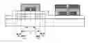
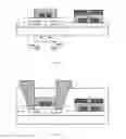
As shown in FIGS. 1 and 2, the present disclosure provides in some embodiments a method for manufacturing an array substrate, which includes steps of: forming a semiconductor pattern 2, a gate electrode 4 and a first insulation pattern 5 sequentially on a base substrate 1 at different layers, the semiconductor pattern 2 being insulated from the gate electrode 4, an orthogonal projection C of the semiconductor pattern 2 onto the base substrate 1 covering an orthogonal projection B of the first insulation pattern 5 onto the base substrate 1, and the orthogonal projection B of the first insulation pattern 5 onto the base substrate 1 covering an orthogonal projection A of the gate electrode 4 onto the base substrate 1; and subjecting the semiconductor pattern 2 to ion implantation through a single ion implantation process using the first insulation pattern 5 and the gate electrode 4 as a mask plate, so as to form an active layer 2C, a heavily-doped source electrode region 2A, a lightly-doped source electrode region 2B, a heavily-doped drain electrode region 2D, and a lightly-doped drain electrode region 2E.
Subsequent to the ion implantation, an orthogonal projection of the active layer 2C onto the base substrate 1 fully overlaps the orthogonal projection A of the gate electrode 4 onto the base substrate 1, orthogonal projections El, E2 of the lightly-doped source electrode region 2B and the lightly-doped drain electrode region 2D onto the base substrate 1 overlaps the orthogonal projection B of the first insulation pattern 5 onto the base substrate 1 rather than the orthogonal projection A of the gate electrode 4 onto the base substrate 1, and orthogonal projections D1, D2 of the heavily-doped source electrode region 2A and the heavily-doped drain electrode region 2E onto the base substrate 1 do not overlap the orthogonal projection B of the first insulation pattern 5 onto the base substrate 1 and the orthogonal projection A of the gate electrode 4 onto the base substrate 1.
According to the method in the embodiments of the present disclosure, a source electrode and a drain electrode each having the lightly-doped region and heavily-doped region may be formed merely through a single ion implantation process. In this way, it is able to reduce the manufacturing time, thereby to reduce the manufacture cost. In addition, through the lightly-doped regions and heavily-doped regions, it is able to reduce the drain current, thereby to improve the operation stability of a display panel.
During the manufacture, for the array substrate with a low-temperature poly-Si TFT, a storage capacitor (Cs) also needs to be provided, so as to meet the requirement of driving liquid crystals. The storage capacitor includes an upper polar plate, a lower polar plate, and a second insulation pattern for separating the upper polar plate from the lower polar plate. Currently, the lower polar plate of the storage capacitor also needs to be formed after the ion implantation. The semiconductor pattern of the TFT is located at a region different from the lower polar plate of the storage capacitor, so in the related art, two ion implantation processes with different mask plates need to be adopted, and the ion implantation processes may be time-consuming. In order to improve the manufacture efficiency and reduce the manufacture cost, the lower polar plate of the storage capacitor may be formed in an identical ion implantation process.
The method will be described hereinafter in more details in conjunction with FIG. 3.
As shown in FIG. 3, the method for manufacturing the array substrate with the low-temperature poly-Si TFT may include the following steps.
Step 1: as shown in FIG. 3A, forming the semiconductor pattern 2 on the base substrate 1. The semiconductor pattern 2 may have a thickness of 100 Å to 3000 Å, and optionally 500 Å to 1000 Å. To be specific, a semiconductor material layer may be deposited onto the base substrate 1 through plasma enhanced chemical vapor deposition (PECVD), low-pressure chemical vapor deposition (LPCVD) or sputtering, and then treated with a patterning process, so as to form the semiconductor pattern 2.
Of course, optionally, a buffer layer may be deposited onto the base substrate 1, and then the semiconductor pattern 2 may be formed subsequently. The buffer layer functions as to prevent impurities in the base substrate 1 from entering the active layer of the TFT, thereby to prevent characteristics of the TFT, e.g., a threshold voltage and a leakage current, from being changed.
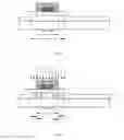
Step 2: as shown in FIG. 3B, forming a first insulation layer 3 on the base substrate 1 with the semiconductor pattern 2. The first insulation layer 3 may be of a single layer made of silicon dioxide or silicon nitride, or a double-layered structure consisting of the two layers. According to the practical need, the first insulation layer 3 may have a thickness of 500 Å to 2000 Å, optionally 600 Å to 1500 Å.
Step 3: as shown in FIG. 3C, forming the gate electrode 4 and the lower polar plate 4a made of an identical material and arranged at an identical layer on the base substrate 1 with the first insulation layer 3. The gate electrode 4 and the lower polar plate 4a may each be of a structure consisting of one, two or more layers. They may be made of metal or a metal alloy, e.g., molybdenum, aluminum, or a molybdenum-tungsten alloy. The gate electrode 4 and the lower polar plate 4a may each have a thickness of 1000 Å to 5000 Å, optionally 1500 Å to 4000 Å.
Step 4: as shown in FIG. 3D, forming a first insulation pattern 5 and a second insulation pattern 5a on the base substrate 1 with the gate electrode 4 and the lower polar plate 4a, and the first insulation pattern 5 and the second insulation pattern 5a being created from a second insulation layer. The first insulation pattern 5 covers the gate electrode 4, and the second insulation pattern 5a covers the lower polar plate 4a. The second insulation layer may be formed in a way identical to the first insulation layer 3.
It should be appreciated that, for the conventional TFT, a gate insulation layer for protection, i.e., the second insulation layer, may be arranged above the gate electrode, and the entire second insulation layer may be formed merely through deposition. However, in the embodiments of the present disclosure, the second insulation layer further needs to be treated by a patterning process, so as to form the first insulation pattern 5 which may serve as a mask plate during the ion implantation.
Step 5: as shown in FIG. 3E, subjecting the semiconductor pattern to ion implantation through a single ion implantation process using the first insulation pattern 5 and the gate electrode 4 as a mask plate, so as to form the active layer 2C, the heavily-doped source electrode region 2A, the lightly-doped source electrode region 2B, the heavily-doped drain electrode region 2D and the lightly-doped drain electrode region 2E. In addition, during the ion implantation, ions may also be implanted into the lower polar plate 4a. The ion implantation is performed using a gas containing boron and/or phosphorus as an implantation media, at an implantation energy of 10 to 200 KeV and at an implantation dosage of 1*1011 to 1*1020 atoms/cm3.
During the ion implantation, it is able to block a part of the ions by each of the first insulation pattern 5 and the gate electrode 4, and through the cooperation of them, it is able to block all the ions. Through the first insulation pattern 5 and the gate electrode 4, it is able to form a half-blocking mask plate, a fully-blocking mask plate and an unblocking mask plate with different ion-implantation rates, thereby to provide the semiconductor pattern with three regions with different conductivities, i.e., the heavily-doped region with the highest conductivity, the lightly-doped region with the second highest conductivity, and the active layer with the lowest conductivity.
Step 6: as shown in FIG. 3F, forming the upper polar plate 6a of the storage capacitor on the second insulation pattern 5a. In order to reduce the manufacture cost, the upper polar plate 6a may be formed using the mask plate that has been used to form the first insulation pattern 5 and the second insulation pattern 5a. In this way, the upper polar plate 6a of the storage capacitor may have a pattern identical to that of the second insulation pattern 5a, and a layer made of a material identical to the upper polar plate 6a, i.e., a conductive pattern 6 identical to the first insulation pattern 5, may not be etched off and thus reserved above the first insulation pattern 5 (the conductive pattern 6 may be or may not be removed).
The above are the illustrative steps of the method for manufacturing the array substrate. As compared with the related art, it is able for the method in the embodiments of the present disclosure to, merely through a single ion implantation process, form the heavily-doped region and the lightly-doped region on each of the source electrode and the drain electrode of the TFT, and meanwhile subject the lower polar plate of the storage capacitor to the ion implantation. In addition, in the embodiments of the present disclosure, although the second insulation layer covering the gate electrode and the lower polar plate needs to be treated through a patterning process, it may share an identical mask plate with the upper polar plate 6a, i.e., it is unnecessary to provide an additional mask plate as compared with the related art.
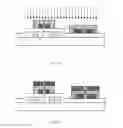
Of course, referring to FIG. 5, the method may further include forming a third insulation layer 7, forming via-holes in the third insulation layer 7, and then forming conductive patterns 8, 9. The conductive pattern 8 may be connected to the heavily-doped source electrode region 2A through one of the via-holes in the third insulation layer 7, so as to form the source electrode of the TFT together with the heavily-doped source electrode region 2A and the lightly-doped source electrode region 2B. Identically, the conductive pattern 9 may be connected to the heavily-doped drain electrode region 2E through the other of the via-holes in the third insulation layer 7, so as to form the drain electrode of the TFT together with the heavily-doped drain electrode region 2E and the lightly-doped drain electrode region 2D.
As shown in FIG. 4, the present disclosure provides in some embodiments an array substrate manufactured by the above-mentioned method. The array substrate includes: a base substrate 1, and a TFT formed on the base substrate 1. The TFT includes a gate electrode 4, a source electrode, a drain electrode and an active layer 2C. The source electrode includes a heavily-doped source electrode region 2A and a lightly-doped source electrode region 2B, and the drain electrode includes a heavily-doped drain electrode region 2D and a lightly-doped drain electrode region 2E. The array substrate further includes a first insulation pattern 5 which is arranged above the gate electrode 4, and an orthogonal projection B of which onto the base substrate 1 covers an orthogonal projection A of the gate electrode e onto the base substrate 1.
An orthogonal projection of the active layer 2C onto the base substrate 1 fully overlaps the orthogonal projection A of the gate electrode 4 onto the base substrate 1, orthogonal projections E1, E2 of the lightly-doped source electrode region 2B and the lightly-doped drain electrode region 2D onto the base substrate 1 overlap the orthogonal projection B of the first insulation pattern 5 onto the base substrate 1 rather than the orthogonal projection A of the gate electrode 4 onto the base substrate 1, and orthogonal projections D1, D2 of the heavily-doped source electrode region 2A and the heavily-doped drain electrode region 2E onto the base substrate 1 do not overlap the orthogonal projection B of the first insulation pattern 5 onto the base substrate 1 and the orthogonal projection A of the gate electrode 4 onto the base substrate 1.
According to the array substrate in the embodiments of the present disclosure, the source electrode and the drain electrode each having the lightly-doped region and heavily-doped region may be formed merely through a single ion implantation process. In this way, it is able to reduce the manufacturing time, thereby to reduce the manufacture cost.
In the embodiments of the present disclosure, the array substrate further includes a storage capacitor formed on the base substrate 1. The storage capacitor includes an upper polar plate 6a, a lower polar plate 4a, and a second insulation pattern 5a for separating the upper polar plate 6a from the lower polar plate 4a. The upper polar plate 4a is made of an identical material and arranged at an identical layer to the gate electrode 4, and the first insulation pattern 5 is made of an identical material and arranged at an identical layer to the second insulation pattern 5a.
Referring to FIG. 5, the array substrate further includes a third insulation layer 7 with via-holes, and conductive patterns 8, 9.
The conductive pattern 8 is connected to the heavily-doped source electrode region 2A through one of the via-holes in the third insulation layer 7, so as to form the source electrode of the TFT together with the heavily-doped source electrode region 2A and the lightly-doped source electrode region 2B. Identically, the conductive pattern 9 is connected to the heavily-doped drain electrode region 2E through the other of the via-holes in the third insulation layer 7, so as to form the drain electrode of the TFT together with the heavily-doped drain electrode region 2E and the lightly-doped drain electrode region 2D.
The present disclosure further provides in some embodiments a display device including the above-mentioned array substrate. Here, the display device may be a display panel only, or a display device including the display panel. The display device may be any product or member having a display function, such as a liquid crystal panel, a liquid crystal display device, an organic light-emitting diode (OLED) display panel, an OLED display device, an electronic paper, or a digital photo frame.
The above are merely the preferred embodiments of the present disclosure. Obviously, a person skilled in the art may make further modifications and improvements without departing from the spirit of the present disclosure, and these modifications and improvements shall also fall within the scope of the present disclosure.
Claims
1. A method for manufacturing an array substrate, comprising steps of:
forming a semiconductor pattern, a gate electrode and a first insulation pattern sequentially on a base substrate at different layers, the semiconductor pattern being insulated from the gate electrode, an orthogonal projection of the semiconductor pattern onto the base substrate covering an orthogonal projection of the first insulation pattern onto the base substrate, and the orthogonal projection of the first insulation pattern onto the base substrate covering an orthogonal projection of the gate electrode onto the base substrate; and
subjecting the semiconductor pattern to ion implantation through a single ion implantation process using the first insulation pattern and the gate electrode as a mask plate, to form an active layer, a heavily-doped source electrode region, a lightly-doped source electrode region, a heavily-doped drain electrode region, and a lightly-doped drain electrode region,
wherein subsequent to the ion implantation, an orthogonal projection of the active layer onto the base substrate fully overlaps the orthogonal projection of the gate electrode onto the base substrate, orthogonal projections of the lightly-doped source electrode region and the lightly-doped drain electrode region onto the base substrate overlap the orthogonal projection of the first insulation pattern onto the base substrate rather than the orthogonal projection of the gate electrode onto the base substrate, and orthogonal projections of the heavily-doped source electrode region and the heavily-doped drain electrode region onto the base substrate do not overlap the orthogonal projection of the first insulation pattern onto the base substrate and the orthogonal projection of the gate electrode onto the base substrate.
2. The method according to claim 1, further comprising forming a storage capacitor including an upper polar plate, a lower polar plate, and a second insulation pattern for separating the upper polar plate from the lower polar plate, wherein the lower polar plate is made of an identical material and arranged at an identical layer to the gate electrode, and the first insulation pattern is made of an identical material and arranged at an identical layer to the second insulation pattern.
3. The method according to claim 2, further comprising:
forming the semiconductor pattern on the base substrate;
forming a first insulation layer on the base substrate with the semiconductor pattern;
forming the gate electrode and the lower polar plate made of an identical material and arranged at an identical layer on the base substrate with the first insulation layer;
forming the first insulation pattern and the second insulation pattern made of the second insulation layer on the base substrate with the gate electrode and the lower polar plate, the first insulation pattern covering the gate electrode, and the second insulation pattern covering the lower polar plate;
subjecting the semiconductor pattern to ion implantation through a single ion implantation process using the first insulation pattern and the gate electrode as a mask plate, to form the active layer, the heavily-doped source electrode region and the lightly-doped source electrode region, and the heavily-doped drain electrode region and the lightly-doped drain electrode region; and
forming the upper polar plate on the second insulation pattern.
4. The method according to claim 2, wherein a patterning process for forming the first insulation pattern and the second insulation pattern and a patterning process for forming the upper polar plate use a same mask plate.
5. The method according to claim 1, wherein the gate electrode is made of molybdenum and/or aluminum, and has a thickness of 1000 Å to 5000 Å.
6. The method according to claim 5, wherein the gate electrode has a thickness of 1500 Å to 4000 Å.
7. The method according to claim 3, wherein the first insulation layer is made of silicon dioxide and/or silicon nitride, and has a thickness of 500 Å to 2000 Å.
8. The method according to claim 7, wherein the first insulation layer has a thickness of 600 Å to 1500 Å.
9. The method according to claim 1, wherein the ion implantation is performed using a gas containing boron and/or phosphorus as an implantation media, at an implantation energy of 10 to 200 KeV and at an implantation dosage of 1*1011 to 1*1020 atoms/cm3.
10. An array substrate, comprising:
a base substrate,
a thin film transistor (TFT) formed on the base substrate, the TFT comprising a gate electrode, a source electrode, a drain electrode and an active layer, the source electrode comprising a heavily-doped source electrode region and a lightly-doped source electrode region, and the drain electrode comprising a heavily-doped drain electrode region and a lightly-doped drain electrode region; and
a first insulation pattern arranged above the gate electrode, and an orthogonal projection of the first insulation pattern onto the base substrate covering an orthogonal projection of the gate electrode onto the base substrate,
wherein an orthogonal projection of the active layer onto the base substrate fully overlaps the orthogonal projection of the gate electrode onto the base substrate, orthogonal projections of the lightly-doped source electrode region and the lightly-doped drain electrode region onto the base substrate overlap the orthogonal projection of the first insulation pattern onto the base substrate rather than the orthogonal projection of the gate electrode onto the base substrate, and orthogonal projections of the heavily-doped source electrode region and the heavily-doped drain electrode region onto the base substrate do not overlap the orthogonal projection of the first insulation pattern onto the base substrate and the orthogonal projection of the gate electrode onto the base substrate.
11. The array substrate according to claim 10, further comprising a storage capacitor formed on the base substrate, wherein the storage capacitor comprises an upper polar plate, a lower polar plate, a second insulation pattern for separating the upper polar plate from the lower polar plate, the lower polar plate is made of an identical material and arranged at an identical layer to the gate electrode, and the first insulation pattern is made of an identical material and arranged at an identical layer to the second insulation pattern.
12. The array substrate according to claim 10, wherein the gate electrode is made of molybdenum and/or aluminum, and has a thickness of 1000 Å to 5000 Å.
13. The array substrate according to claim 12, wherein the gate electrode has a thickness of 1500 Å to 4000 Å.
14. The array substrate according to claim 11, wherein the lower polar plate and the gate electrode is each of a structure consisting of one, two or more layers.
15. A display device, comprising the array substrate according to claim 10.
16. The method according to claim 3, wherein a patterning process for forming the first insulation pattern and the second insulation pattern and a patterning process for forming the upper polar plate use a same mask plate.
17. The method according to claim 2, wherein the gate electrode is made of molybdenum and/or aluminum, and has a thickness of 1000 Å to 5000 Å.
18. The method according to claim 3, wherein the gate electrode is made of molybdenum and/or aluminum, and has a thickness of 1000 Å to 5000 Å.
19. The method according to claim 4, wherein the gate electrode is made of molybdenum and/or aluminum, and has a thickness of 1000 Å to 5000 Å.
20. The method according to claim 4, wherein the first insulation layer is made of silicon dioxide and/or silicon nitride, and has a thickness of 500 Å to 2000 Å.
Images & Drawings included:
Sources:
- United States Patent and Trademark Office - verify current appl. status at the USPTO↗
Similar patent applications:
- » 20180159066
Array substrate, display panel, display device, method for manufacturing array substrate and method for manufacturing display panel - » 20060086937
Tft array substrate, liquid crystal display device, manufacturing methods of tft array substrate and liquid crystal display device, and electronic device - » 20150021612
Array substrate, display device and manufacturing method of array substrate - » 20180175078
Array substrate, display device and manufacturing method for array substrate - » 20160035573
Array substrate, display device, and manufacturing method of array substrate - » 20160071834
Array substrate, display device and manufacturing method of array substrate - » 20180012885
Array substrate, display device and manufacturing method of array substrate - » 20160327840
Array substrate, display device and method for manufacturing array substrate - » 20160211277
Array substrate, display device and manufacturing method of the array substrate - » 20160291417
Array substrate, display device and method for manufacturing array substrate
Recent applications in this class:
- » 20250291221 2025-09-18
DISPLAY DEVICE INCLUDING A STRIP OXIDE SEMICONDUCTOR OVERLAPPING AN OPENING - » 20250284165 2025-09-11
ELECTRO-OPTICAL DEVICE AND ELECTRONIC APPARATUS - » 20250284164 2025-09-11
ELECTRO-OPTICAL DEVICE AND ELECTRONIC APPARATUS - » 20250278003 2025-09-04
ARRAY SUBSTRATE AND DISPLAY PANEL - » 20250271718 2025-08-28
PIXEL ELECTRODE, ARRAY SUBSTRATE AND DISPLAY DEVICE - » 20250271717 2025-08-28
DISPLAY SUBSTRATE, DISPLAY PANEL AND DISPLAY DEVICE - » 20250258413 2025-08-14
ARRAY SUBSTRATE AND MANUFACTURING METHOD THEREFOR, AND DISPLAY APPARATUS - » 20250244628 2025-07-31
DISPLAY DEVICE - » 20250244627 2025-07-31
DISPLAY APPARATUS AND ARRAY SUBSTRATE - » 20250237917 2025-07-24
DISPLAY PANEL AND DISPLAY APPARATUS
Recent applications for this Assignee:
- » 20250295022 2025-09-18
QUANTUM DOT COMPOSITION, LIGHT-EMITTING ELEMENT, DISPLAY PANEL AND PREPARATION METHOD THEREOF - » 20250295019 2025-09-18
HEAT DISSIPATION FILM, DISPLAY MODULE AND DISPLAY DEVICE - » 20250294987 2025-09-18
DISPLAY PANEL, DISPLAY DEVICE - » 20250294983 2025-09-18
DISPLAY PANEL AND DISPLAY DEVICE - » 20250292736 2025-09-18
DRIVING CIRCUIT, DRIVING METHOD, DRIVING MODULE AND DISPLAY DEVICE - » 20250291336 2025-09-18
COMPUTER-IMPLEMENTED METHOD, APPARATUS FOR MANAGING PRODUCTION OF ONE OR MORE PRODUCTS, AND COMPUTER-PROGRAM PRODUCT - » 20250291215 2025-09-18
CIRCUIT BOARD AND METHOD FOR MANUFACTURING THE SAME, LIGHT-EMITTING SUBSTRATE, BACKLIGHT MODULE, DISPLAY PANEL AND DISPLAY APPARATUS - » 20250287801 2025-09-11
ARRAY SUBSTRATE AND DISPLAY APPARATUS - » 20250287695 2025-09-11
ARRAY PANEL, METHOD OF MANUFACTURING THE SAME AND DISPLAY DEVICE - » 20250285597 2025-09-11
DISPLAY SUBSTRATE AND DISPLAY DEVICE