Variable frequency oscillator having wide tuning range and low phase noise
US20170201213A1
2017-07-13
15/399,059
2017-01-05
✅ Patent granted
US 10,374,549 B2
2019-08-06
-
-
Arnold M Kinkead
Robert W. Morris | Ojeiku C. Aisiku | Eckert Seamans Cherin & Mellott, LLC
2037-06-15
Abstract:
A variable frequency oscillator comprising a first transistor (10) and a second transistor (20); wherein the first transistor (10) has a first terminal—collector—which is connected to a reference voltage, and a second terminal—emitter—which is connected to a first terminal of a first current source (13), which second terminal is connected to ground, and a third terminal—base—connected to a first terminal of a first inductor (14) and to a top terminal of a first capacitor (11), wherein the first capacitor (11) has a bottom terminal which is connected to the second terminal—emitter—of the first transistor (10) but also to a top terminal of a second capacitor (12) having a bottom terminal being connected to ground;
-
- wherein the second transistor (20) has a first terminal—collector—which is connected to a reference voltage, and a second terminal—emitter—which is connected to a first terminal of a second current source (23), which second terminal is connected to ground, and a third terminal—base—connected to a first terminal of a second inductor (14) and to a top terminal of a third capacitor (21), wherein the third capacitor (21) has a bottom terminal which is connected to the second terminal—emitter—of the second transistor (20) and also to a top terminal of a fourth capacitor (22) having a bottom terminal connected to ground;
- wherein the first and second inductors (14, 24) have a second terminal which are connected via a circuit (100) achieving variable capacitance, so as to form a circuit connecting in series all passive components composing the LC tank, so as to achieve a variable capacitance which can be used for performing a tuning of the oscillator, and
- wherein the second capacitor (12) and the fourth capacitor (22) are both connected to the physical ground thereby avoiding a 2nd harmonic common mode oscillation that might dominate over the differential fundamental one and might destroy the first and the second transistors (10, 20).
Inventors:
- BIAGIO BISANTI 11 🇫🇷 ANTIBES, France
- ERIC DUVIVIER 2 🇫🇷 VALLAURIS GOLFE JUAN, France
- LORENZO CARPINETO 5 🇫🇷 ANTIBES, France
- STEFANO CIPRIANI 2 🇫🇷 ANTIBES, France
- FRANCESCO COPPOLA 6 🇫🇷 GRASSE, France
- GIANNI PUCCIO 6 🇫🇷 LA GAUDE, France
- RÉMI ARTINIAN 1 🇫🇷 ANTIBES, France
- FRANCOIS MAROT 2 🇫🇷 ANTIBES, France
- VANESSA BEDERO 2 🇫🇷 VENCE, France
- LYSIANE KOECHLIN 2 🇫🇷 VALLAURIS, France
- REMI ARTINIAN 2 🇫🇷 ANTIBES, France
Assignee:
- SDRF EURl 2 🇫🇷 Sophia Antipolis, Biot, France
Applicant:
Interested in similar patents?
Get notified when new applications in this technology area are published.
Classification:
H03B5/12 IPC
Generation of oscillations using amplifier with regenerative feedback from output to input with frequency-determining element comprising lumped inductance and capacitance active element in amplifier being semiconductor device
H03B5/124 » CPC further
Generation of oscillations using amplifier with regenerative feedback from output to input with frequency-determining element comprising lumped inductance and capacitance active element in amplifier being semiconductor device comprising means for varying the frequency of the generator the means comprising a voltage dependent capacitance
H03B5/1231 » CPC further
Generation of oscillations using amplifier with regenerative feedback from output to input with frequency-determining element comprising lumped inductance and capacitance active element in amplifier being semiconductor device the amplifier comprising one or more bipolar transistors
H03B2200/004 » CPC further
Indexing scheme relating to details of oscillators covered by; Circuit elements of oscillators including a variable capacitance, e.g. a varicap, a varactor or a variable capacitance of a diode or transistor
H03B2201/0208 » CPC further
Aspects of oscillators relating to varying the frequency of the oscillations; Varying the frequency of the oscillations by electronic means the means being an element with a variable capacitance, e.g. capacitance diode
H03B5/04 » CPC main
Generation of oscillations using amplifier with regenerative feedback from output to input; Details Modifications of generator to compensate for variations in physical values, e.g. power supply, load, temperature
H03B5/1218 » CPC further
Generation of oscillations using amplifier with regenerative feedback from output to input with frequency-determining element comprising lumped inductance and capacitance active element in amplifier being semiconductor device using multiple transistors for amplification the generator being of the balanced type
H03B2200/0006 » CPC further
Indexing scheme relating to details of oscillators covered by; Types of oscillators Clapp oscillator
H03B5/1243 » CPC further
Generation of oscillations using amplifier with regenerative feedback from output to input with frequency-determining element comprising lumped inductance and capacitance active element in amplifier being semiconductor device comprising means for varying the frequency of the generator the means comprising a voltage dependent capacitance the means comprising voltage variable capacitance diodes
H03B2200/0008 » CPC further
Indexing scheme relating to details of oscillators covered by; Types of oscillators Colpitts oscillator
H03L7/099 » CPC further
Automatic control of frequency or phase; Synchronisation using a reference signal applied to a frequency- or phase-locked loop; Details of the phase-locked loop concerning mainly the controlled oscillator of the loop
Description
TECHNICAL FIELD
The invention relates to the field of electronics circuits and more particularly to a wide range voltage control oscillator showing low phase noise.
BACKGROUND ART
Oscillator circuits play quite an important part in the field of electronics circuits, including communication systems, providing clocking and timing signals in digital circuits and frequency translation in radio frequency (RF) circuits.
Among those oscillators, the well-known Colpitts oscillator is widely used in the field. An example of a Colpitts oscillator is illustrated in FIG. 1A showing a transistor M biased by a current source I and associated with an inductance L and the series combination of C1 and C2 capacitors forming the parallel resonant tank circuit defining the oscillation frequency, in accordance with the formula.
f = 1 2 π L ( C 1 C 2 C 1 + C 2 )
In the Colpitts circuits, the arrangement of a variable frequency oscillator (VFO) requires the voltage divider to include a variable capacitor (either C1 or C2), thus causing the feedback voltage to be variable as well.
A variant of the Colpitts circuit, the well-known Clapp oscillator, avoids this problem by using two fixed capacitors C1 and C2, with a variable Capacitor which is arranged in series with the inductor, as shown in FIG. 2A, and which oscillates at the following frequency:
f = 1 2 π 1 L ( 1 C 0 + 1 C 1 + 1 C 2 )
The Clapp oscillator is quite often used in association with a varactor, as illustrated in FIG. 2, which is based on a reversely biased diod forming the variable capacitor.
There are other oscillation circuits well-known in the art, and particular those based on a differential topology, such as the well-known cross-coupled differential architecture.
Generally speaking, all those conventional architectures are sensitive to parasitic capacitances which might impair the possibility of achieving, at the same time, a wide tuning range together with a low noise.
Therefore, there is a desire for a new topology of a variable frequency oscillator (F) or a voltage controlled oscillator (VCO) which achieves those goals.
SUMMARY OF THE INVENTION
It is an object of the present invention to provide a variable frequency oscillator (VFO) or a voltage controlled oscillator (VCO) which allows wide tuning range and low phase noise.
It is a further object of the present invention to provide a variable frequency oscillator (VFO), based on the Colpitts or Clapp topology, and which is less sensitive to parasitic capacitances.
It is still another object of the present invention to achieve a variable frequency oscillator (VFO) which can be configured for allowing both digital and analog tuning.
These and other objects of the invention are achieved by means of a variable Frequency oscillator comprising a first transistor and a second transistor, which may be for instance NPN transistors.
The first transistor has a first terminal (e.g. collector) which is connected to a reference voltage, and a second terminal (e.g. emitter) which is connected to a first terminal of a first current source which second terminal is connected to ground. The first transistor further has a third terminal (e.g. base) which is connected to a first terminal of a first inductor and to a top terminal of a first capacitor C1 having a bottom terminal being connected to the emitter of the first transistor and also to a top terminal of a second capacitor C2 having a bottom terminal being connected to ground.
The second transistor has a first terminal (e.g. collector) which is connected to a reference voltage, and a second terminal (e.g. emitter) which is connected to a first terminal of a second current source which second terminal is connected to ground. The second transistor has a third terminal connected to a first terminal of a second inductor and to a top terminal of a third capacitor (C1), wherein the third capacitor has a bottom terminal which is connected to the second terminal (emitter) of the second transistor and also to a top terminal of a fourth capacitor (C2) having a bottom terminal being connected to ground.
In order to achieve a variable frequency oscillation between the emitters (Outn, Outp) of the two transistors 10, 20, a variable tank capacitors is connected between the second terminal of inductors (14, 24), so as to form a circuit connecting in series all passive components composing the LC tank, thus masking most of parasitic capacitances. Consequently, the variable frequency oscillator may be used at a very high frequency.
In one embodiment, the circuit connecting the first and second inductors comprises two varactors connected in series with two capacitors so as to achieve analog control of the oscillation frequency.
Preferably, the varactors are sized so as to compensate temperature variation within the tuning range.
In one embodiment, the circuit connecting the first and second inductors comprises a bank of capacitors arranged in several paths connected in parallel, wherein each path comprises two capacitors connected in series with a switching component, wherein the switching components of all paths are controlled by means of a programmed tank Calibration Word (CW), so as to achieve the tuning of the oscillation frequency.
Preferably, the bank of capacitors comprised within the circuit connecting the inductors is configured so as to allow coarse and fine digital control of the oscillation frequency.
DESCRIPTION OF THE DRAWINGS
Other features of one or more embodiments of the invention will appear from the following description of embodiments of the invention, with reference being made to the accompanying drawings.
FIG. 1a illustrates a first known variable frequency oscillator (VFO) according to the well-known Colpitts topology.
FIG. 1b illustrates a second known variable frequency oscillator (VFO) which complies with the Clapp technology.
FIG. 2 illustrates a variant of a known variable frequency oscillator of FIG. 1b, which further uses a varactor.
FIG. 3 illustrates one embodiment of a variable frequency oscillator (VFO) of the present invention.
DESCRIPTION OF THE PREFERRED EMBODIMENT
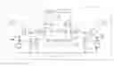
With respect to FIG. 3, there is now described the general architecture of a variable frequency oscillator (VFO) or voltage control oscillator (VCO) which is well adapted for carrying out the RF circuitry of a communication system, with low phase noise and wide tuning range.
For the sake of clarity, FIG. 3 shows the arrangement with simplified biasing so as to focus on the main elements of the preferred embodiments.
The architecture is based on a differential topology comprising a first transistor 10 and a second transistor 20 which, in the embodiment being considered are conventional NPN transistors.
It should be clear that a skilled man will be able to replace transistors 10 and 20 by other transistors, including FET transistors, MOS transistors etc . . .
Transistor 10 has an emitter generating a first output signal Outp, a base and a collector. The collector of transistor 10 is connected to a reference voltage, serving as a ground for AC.
a. The emitter of transistor 10 is connected to a first terminal of a first current source 13 having a second terminal connected to ground. The base of transistor 10 is connected to a first terminal of a first inductor 14, and also to the top terminal of a first capacitor 11, having a value of C1. Capacitor 11 has a bottom terminal which is connected to the emitter of transistor 10 but also to a top terminal of a second capacitor 12, having a value C2. Capacitor 12 has a bottom terminal which is connected to ground.
b. Similarly, transistor 20 is based on a Colpitts topology with a feedback network based on a third and a fourth capacitor, respectively of values C1 and C2. More particularly, the emitter of transistor 20 generates a second output signal Outn and is connected to a first terminal of a second current source 23 having a second terminal connected to ground. The base of transistor 20 is connected to a first terminal of a second inductor 24, and also to the top terminal of a third capacitor 21, having a value equal to C1. Capacitor 21 has a bottom terminal which is connected to the emitter of transistor 20 and also to a top terminal of a fourth capacitor 22, having a value C2. Capacitor 22 has a bottom terminal which is connected to ground.
It can be seen that the feedback capacitors 12 and 22 have both their bottom terminal being connected to ground in order to isolate the two transistors 10 and 20. In fact if capacitors 12 and 22 (C2) were connected between the two emitters there would be a 2nd harmonic common mode oscillation building up that dominates over the differential fundamental one and might increase the Phase Noise (PN). This is quite an advantageous effect from the arrangement of FIG. 3, which is highly more effective than the use of a convention ‘virtual ground”.
In the embodiment which is represented in FIG. 3, first and second inductors 14 and 24 both have a second terminal which are connected via a circuit 100 achieving variable capacitance, so as to form a circuit connecting in series all passive components composing the LC tank: capacitors 11, 12, 22, 21 and the two inductors 14 and 24.
With the consequence that the series connection of all capacitors allows the masking of parasitic capacitances, which was not possible with the conventional topology where the capacitors are viewed in parallel.
In fact—and this observation is true not only for the single ended circuit but also for the differential one, the negative impedance given by the transistor 10 and the capacitor 11 and 12 is (in first approximation)
Z in = - i * w * C 1 * C 2 C 1 + C 2 - gm w 2 * ( C 1 + C 2 ) C core = C 1 * C 2 C 1 + C 2
From the equation reported above one sees that the Ccore will play un important role in determining the final VCO frequency. If the inductor is connected in parallel with the tuning capacitor we need Ccore to be small compared to the tuning capacitor to increase the tuning range. If on the other end, the inductor is connected in series with the tuning capacitor, as reported in FIG. 3, the bigger Ccore is the more the tuning range approaches the limit the tuning capacitor can achieve. This clearly shows the advantage of working with higher value capacitor and stay away of the physical
Circuit 100 allowing the connection in series of inductors 14 and 24 may take several forms.
In one embodiment, circuit 100 comprises two varactors 16 and 26 connected in series, with their two cathode terminal being connected together, and being further connected in series with two capacitors 15 and 25, so as to achieve a variable capacitance which can be used for performing a tuning of the oscillator. Control of the varactors can be achieved by applying a voltage control at the common cathode terminal of both varactors. In one embodiment, the varactors are sized to compensate with its tuning range the temperature variation and assure that the VCO can lock to the programmed frequency and keep the lock over temperature if locked around a predefined voltage window. The voltage window will move according to the locking temperature.
In one other embodiment, circuit 100 may further comprising a bank of capacitors tank arranged in several paths connected in parallel, respectively 101-102, 111-112, . . . , 191-192, each individual path comprising two capacitors connected in series with a switching component. As seen in FIG. 3, circuit 100 may comprise a first path comprising capacitors 101 and 102 connected in series with a first switching component 103. Furthermore, circuit 100 may comprise a second path comprising capacitors 111 and 112 connected in series with a second switching component 113 . . . FIG. 3 further illustrates a nth path comprising capacitors 191 and 192 connected series with a nth switching component 193 . . .
It can be seen that the bank of capacitors comprised within circuit 101 can be controlled by means of programmed tank Calibration Word (CW) which can be used for the purpose of independently controlling the switches 103, 113, . . . 193 . . . Thanks to such arranged, digital control of the frequency oscillation can be achieved.
In one embodiment, the bank of capacitors forming the tank's capacitor bank of circuit 100 is made by a coarse and fine bank. The capacitors in the coarse and fine bank are of different type therefore an important overlap was considered between the coarse and fine range. The coarse bank is a 5 bit binary weighted capacitive MIM bank (Metal Insulator Metal . . . ) whereas fine bank is a three bits binary weighted Metal Fringe bank (except for the lower frequency VCO where both banks are MIM).
Control of the oscillation frequency can also be performed via an analog control, which can be done by applying a control voltage at the common cathode of varactors 16 and 26.
As mentioned previously, the circuit of FIG. 3 is simplified and does not show all components that might be useful for the biasing of the transistors. However, such components are well known to a skilled man and do not need any further development. It suffices to say that, in one embodiment, the bias current of both transistors is set by a resistor (not shown in FIG. 3) whose value can be programmed: the resistor value changes with the programmed tank Calibration Word (CW) applied for the control of switching elements 113, 123, 193, in order to keep the oscillation amplitude constant across the desired VCO digital tuning range.
APPLICATION OF THE INVENTION
The invention may be used for carrying out a VCO to be implemented in a Radio Frequency (RF) circuit of a communication apparatus. When a wide frequency range is to be considered, one may combine several variable frequency oscillator, as described above, in order to combine a circuit which allows wide frequency range.
Such arrangement achieves at the same time good phase noise and wide tuning range working on the Tank's series resonance.
Claims
1. Variable frequency oscillator comprising a first transistor (10) and a second transistor (20);
wherein said first transistor (10) has a first terminal—collector—which is connected to a reference voltage, and a second terminal—emitter—which is connected to a first terminal of a first current source (13) which second terminal is connected to ground, and a third terminal—base—connected to a first terminal of a first inductor (14) and to a top terminal of a first capacitor (11), wherein said first capacitor (11) has a bottom terminal which is connected to said second terminal—emitter—of said first transistor (10) but also to a top terminal of a second capacitor (12) having a bottom terminal being connected to ground;
wherein said second transistor (20) has a first terminal—collector—which is connected to a reference voltage, and a second terminal—emitter—which is connected to a first terminal of a second current source (23) which second terminal) is connected to ground, and a third terminal—base—connected to a first terminal of a second inductor (14) and to a top terminal of a third capacitor (21), wherein said third capacitor (21) has a bottom terminal which is connected to said second terminal—emitter—of said second transistor (20) and also to a top terminal of a fourth capacitor (22) having a bottom terminal being connected to ground;
wherein said first and second inductors (14, 24) have a second terminal which are connected via a circuit (100) achieving variable capacitance, so as to form a circuit connecting in series all passive components composing the LC tank,
so as to achieve a variable capacitance which can be used for performing a tuning of the oscillator; and
wherein said second capacitor (12) and said fourth capacitor (22) are both connected to the physical ground thereby avoiding a 2nd harmonic common mode oscillation that might dominate over the differential fundamental one and might increase the phase noise.
2. Variable frequency oscillator according to claim 1, wherein said circuit (100) connecting said first and second inductor (14, 24) comprises two varactors (16, 28) connected in series with two capacitors (15, 25), wherein each of said varactors (16, 28) has a cathode terminal which is connected to the cathode terminal of said other varactor and to which is applied a control voltage so as to achieve analog control of the oscillation frequency.
3. Variable frequency oscillator according to claim 2, wherein said varactors are sized so as to compensate temperature variation within the tuning range.
4. Variable frequency oscillator according to claim 1, wherein said circuit (100) connecting said first and second inductor (14, 24) comprises a bank of capacitors arranged in several paths (101-102, 111-112, . . . , 191-192), each path comprising two capacitors (101-102, 111-112, . . . 191-192) connected in series with a switching component (103, 113, . . . , 193), wherein the switching components of all paths are controlled by means of a programmed tank Calibration Word (CW), so as to achieve the tuning of the oscillation frequency.
5. Variable frequency oscillator according to claim 4, wherein said bank of capacitors comprised within said circuit (100) connecting said first and second inductors (14, 24) is configured so as to allow coarse and fine digital control of the oscillation frequency.
6. Variable frequency oscillator according to claim 1, wherein said first and second transistors (10, 20) are NPN transistors which first, second and third terminal are respectively a collector, an emitter and a base.
7. Variable frequency oscillator according to claim 1, wherein said first and third capacitors (11, 21) have a value of C1 and said second and fourth capacitors (12, 22) have a value of C2.
Images & Drawings included:


Sources:
- United States Patent and Trademark Office - verify current appl. status at the USPTO↗
Recent applications in this class:
- » 20250274079 2025-08-28
Integrated Circuit Device And Oscillator - » 20250219580 2025-07-03
OSCILLATOR - » 20250219579 2025-07-03
CIRCUIT APPARATUS AND OSCILLATOR - » 20250219578 2025-07-03
CRYSTAL OSCILLATOR BASED ON DUTY RATIO MEASUREMENT - » 20250192722 2025-06-12
Circuit Apparatus And Oscillator - » 20250167731 2025-05-22
Temperature Control Apparatus and Related Device - » 20250088147 2025-03-13
HIGH PRECISION ON-CHIP RC OSCILLATOR - » 20250080050 2025-03-06
DUAL RESONATOR STRUCTURE FOR OVEN-CONTROLLED MEMS OSCILLATORS, INCLUDING RELATED APPARATUSES - » 20250080049 2025-03-06
DUAL RESONATOR STRUCTURE FOR TEMPERATURE-COMPENSATED OSCILLATORS, INCLUDING RELATED APPARATUSES - » 20250080048 2025-03-06
Temperature Stabilized Frequency Control Device