SEMICONDUCTOR DEVICE AND MANUFACTURING METHOD THEREOF
US20170207183A1
2017-07-20
15/249,696
2016-08-29
Abstract:
A semiconductor device includes: a semiconductor substrate; a semiconductor layer on the semiconductor substrate; a source electrode and a drain electrode spaced apart from each other on the semiconductor layer; a gate electrode on the semiconductor layer between the source electrode and the drain electrode; and an insulating film covering the semiconductor layer, the source electrode, the drain electrode and the gate electrode, the gate electrode has an eaves structure including a lower electrode joined to the semiconductor layer and an upper electrode provided on the lower electrode and wider than the lower electrode, a principal ingredient of the insulating film is an oxide film where atomic layers are alternately arrayed for each monolayer, and a film thickness of the insulating film that covers the lower electrode of the gate electrode is equal to a film thickness of the insulating film that covers the upper electrode.
Assignee:
- MITSUBISHI ELECTRIC CORPORATION 16,245 🇯🇵 TOKYO, Japan
Interested in similar patents?
Get notified when new applications in this technology area are published.
Classification:
H01L23/564 » CPC main
Details of semiconductor or other solid state devices Details not otherwise provided for, e.g. protection against moisture
H01L29/408 » CPC further
Semiconductor devices adapted for rectifying, amplifying, oscillating or switching, or capacitors or resistors with at least one potential-jump barrier or surface barrier, e.g. PN junction depletion layer or carrier concentration layer; Details of semiconductor bodies or of electrodes thereof; Multistep manufacturing processes therefor; Electrodes ; Multistep manufacturing processes therefor with an insulating layer with a particular dielectric or electrostatic property, e.g. with static charges or for controlling trapped charges or moving ions, or with a plate acting on the insulator potential or the insulator charges, e.g. for controlling charges effect or potential distribution in the insulating layer, or with a semi-insulating layer contacting directly the semiconductor surface
H01L23/49562 » CPC further
Details of semiconductor or other solid state devices; Arrangements for conducting electric current to or from the solid state body in operation, e.g. leads, terminal arrangements ; Selection of materials therefor consisting of soldered constructions; Lead-frames or other flat leads; Geometry of the lead-frame for devices being provided for in
H01L23/4952 » CPC further
Details of semiconductor or other solid state devices; Arrangements for conducting electric current to or from the solid state body in operation, e.g. leads, terminal arrangements ; Selection of materials therefor consisting of soldered constructions; Lead-frames or other flat leads; Additional leads the additional leads being a bump or a wire
H01L23/3135 » CPC further
Details of semiconductor or other solid state devices; Encapsulations, e.g. encapsulating layers, coatings, e.g. for protection characterised by the arrangement or shape the device being completely enclosed Double encapsulation or coating and encapsulation
H01L29/66848 » CPC further
Semiconductor devices adapted for rectifying, amplifying, oscillating or switching, or capacitors or resistors with at least one potential-jump barrier or surface barrier, e.g. PN junction depletion layer or carrier concentration layer; Details of semiconductor bodies or of electrodes thereof; Multistep manufacturing processes therefor; Types of semiconductor device ; Multistep manufacturing processes therefor; Multistep manufacturing processes of devices having semiconductor bodies comprising group 14 or group 13/15 materials the devices being controllable only by the electric current supplied or the electric potential applied, to an electrode which does not carry the current to be rectified, amplified or switched, e.g. three-terminal devices; Unipolar field-effect transistors with a Schottky gate, i.e. MESFET
H01L21/4825 » CPC further
Processes or apparatus adapted for the manufacture or treatment of semiconductor or solid state devices or of parts thereof; Manufacture or treatment of semiconductor devices or of parts thereof the devices having at least one potential-jump barrier or surface barrier, e.g. PN junction, depletion layer or carrier concentration layer; Manufacture or treatment of parts, e.g. containers, prior to assembly of the devices, using processes not provided for in a single one of the subgroups -; Conductive parts; Flat leads, e.g. lead frames with or without insulating supports Connection or disconnection of other leads to or from flat leads, e.g. wires, bumps, other flat leads
H01L21/565 » CPC further
Processes or apparatus adapted for the manufacture or treatment of semiconductor or solid state devices or of parts thereof; Manufacture or treatment of semiconductor devices or of parts thereof the devices having at least one potential-jump barrier or surface barrier, e.g. PN junction, depletion layer or carrier concentration layer; Assembly of semiconductor devices using processes or apparatus not provided for in a single one of the subgroups - , e.g. sealing of a cap to a base of a container; Encapsulations, e.g. encapsulation layers, coatings Moulds
H01L2223/6683 » CPC further
Details relating to semiconductor or other solid state devices covered by the group; Structural electrical arrangements for semiconductor devices not otherwise provided for; Impedance arrangements; High-frequency adaptations for monolithic microwave integrated circuit [MMIC]
H01L23/00 IPC
Details of semiconductor or other solid state devices
H01L29/40 IPC
Semiconductor devices adapted for rectifying, amplifying, oscillating or switching, or capacitors or resistors with at least one potential-jump barrier or surface barrier, e.g. PN junction depletion layer or carrier concentration layer; Details of semiconductor bodies or of electrodes thereof; Multistep manufacturing processes therefor Electrodes ; Multistep manufacturing processes therefor
H01L23/66 » CPC further
Details of semiconductor or other solid state devices; Structural electrical arrangements for semiconductor devices not otherwise provided for, e.g. in combination with batteries; Impedance arrangements High-frequency adaptations
H01L21/56 IPC
Processes or apparatus adapted for the manufacture or treatment of semiconductor or solid state devices or of parts thereof; Manufacture or treatment of semiconductor devices or of parts thereof the devices having at least one potential-jump barrier or surface barrier, e.g. PN junction, depletion layer or carrier concentration layer; Assembly of semiconductor devices using processes or apparatus not provided for in a single one of the subgroups - , e.g. sealing of a cap to a base of a container Encapsulations, e.g. encapsulation layers, coatings
H01L23/31 IPC
Details of semiconductor or other solid state devices; Encapsulations, e.g. encapsulating layers, coatings, e.g. for protection characterised by the arrangement or shape
H01L29/66 IPC
Semiconductor devices adapted for rectifying, amplifying, oscillating or switching, or capacitors or resistors with at least one potential-jump barrier or surface barrier, e.g. PN junction depletion layer or carrier concentration layer; Details of semiconductor bodies or of electrodes thereof; Multistep manufacturing processes therefor Types of semiconductor device ; Multistep manufacturing processes therefor
H01L21/48 IPC
Processes or apparatus adapted for the manufacture or treatment of semiconductor or solid state devices or of parts thereof; Manufacture or treatment of semiconductor devices or of parts thereof the devices having at least one potential-jump barrier or surface barrier, e.g. PN junction, depletion layer or carrier concentration layer Manufacture or treatment of parts, e.g. containers, prior to assembly of the devices, using processes not provided for in a single one of the subgroups -
H01L29/812 IPC
Semiconductor devices adapted for rectifying, amplifying, oscillating or switching, or capacitors or resistors with at least one potential-jump barrier or surface barrier, e.g. PN junction depletion layer or carrier concentration layer; Details of semiconductor bodies or of electrodes thereof; Multistep manufacturing processes therefor; Types of semiconductor device ; Multistep manufacturing processes therefor controllable by only the electric current supplied, or only the electric potential applied, to an electrode which does not carry the current to be rectified, amplified or switched; Unipolar devices, e.g. field effect transistors; Field effect transistors with field effect produced by a PN or other rectifying junction gate, i.e. potential-jump barrier with a Schottky gate
H01L23/495 IPC
Details of semiconductor or other solid state devices; Arrangements for conducting electric current to or from the solid state body in operation, e.g. leads, terminal arrangements ; Selection of materials therefor consisting of soldered constructions Lead-frames or other flat leads
Description
BACKGROUND OF THE INVENTION
Field
The present invention relates to a semiconductor device and a manufacturing method thereof.
Background
There are FET gate electrodes having an caves structure that includes a lower electrode joined to a semiconductor substrate and an upper electrode wider than the lower electrode. An insulating film that covers the gate electrode having such an eaves structure is conventionally formed using a CVD method. However, since the supply of an insulating film material to the lower part of the eaves decreases, the insulating film that covers the lower electrode becomes thinner than other parts, which reduces a water blocking capability, causing moisture resistance to be more likely to deteriorate. Note that if the gate electrode having the eaves structure is totally embedded with a thick insulating film (e.g., see JP 2015-99865 A), it is possible to prevent the above-described problem with deterioration of moisture resistance.
However, embedding the gate electrode with a thick insulating film to prevent the problem with deterioration of moisture resistance may lead to the problem that the film thickness of the insulating film increases more than necessary, causing the high-frequency characteristic of the FET to deteriorate.
Summary
The present invention has been implemented to solve the above-described problem and it is an object of the present invention to provide a semiconductor device and a manufacturing method thereof capable of preventing deterioration of the moisture resistance and the high-frequency characteristic.
According to the present invention, a semiconductor device includes: a semiconductor substrate; a semiconductor layer on the semiconductor substrate; a source electrode and a drain electrode spaced apart from each other on the semiconductor layer; a gate electrode on the semiconductor layer between the source electrode and the drain electrode; and insulating film covering the semiconductor layer, the source electrode, the drain electrode and the gate electrode, the gate electrode has an eaves structure including a lower electrode joined to the semiconductor layer and an upper electrode provided on the lower electrode and wider than the lower electrode, a principal ingredient of the insulating film is an oxide film where atomic layers are alternately arrayed for each monolayer, and a film thickness of the insulating film that covers the lower electrode of the gate electrode is equal to a film thickness of the insulating film that covers the upper electrode.
In the present invention, a principal ingredient of the insulating film that covers the gate electrode having an eaves structure is an oxide film where atomic layers are alternately arrayed for each monolayer. Furthermore, the film thickness of the insulating film that covers the lower electrode of the gate electrode is equal to the film thickness of the insulating film that covers the upper electrode. Therefore, deterioration of the moisture resistance and the high-frequency characteristic can be prevented.
Other and further objects, features and advantages of the invention will appear more from the following description.
BRIEF DESCRIPTION OF DRAWINGS
FIG. 1 is a cross-sectional view illustrating a semiconductor device according to a first embodiment of the present invention.
FIGS. 2 to 5 are cross-sectional views illustrating the method of manufacturing the semiconductor device according to the first embodiment of the present invention.
FIG. 6 is a cross-sectional view illustrating a semiconductor device according to a comparative example.
FIG. 7 is a cross-sectional view illustrating a semiconductor device according to a second embodiment of the present invention.
FIG. 8 is a plan view illustrating an interior of the semiconductor device according to the second embodiment of the present invention.
FIG. 9 is a cross-sectional view illustrating the semiconductor device in FIG. 7 mounted on a mounting substrate.
DESCRIPTION OF EMBODIMENTS
A semiconductor device and a manufacturing method thereof according to the embodiments of the present invention will be described with reference to the drawings. The same components will be denoted by the same symbols, and the repeated description thereof may be omitted.
First Embodiment
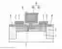
FIG. 1 is a cross-sectional view illustrating a semiconductor device according to a first embodiment of the present invention. A conductive layer 2 and a cap layer 3 are provided on a semiconductor substrate 1. The elements are separated from each other by a nonconductor portion 4. A source electrode 5 and a drain electrode 6 are provided spaced apart from each other on the cap layer 3. The source electrode 5 and the drain electrode 6 are ohmic-joined to the cap layer 3.
Part of the cap layer 3 is removed and a concave portion 7 is formed there. A gate electrode 8 is provided on the conductive layer 2 between the source electrode 5 and the drain electrode 6. An insulating film 9 covers the conductive layer 2, the cap layer 3, the source electrode 5, the drain electrode 6 and the gate electrode 8. The insulating film 9 is in direct contact with at least part of the source electrode 5, the drain electrode 6 and the gate electrode 8.
The gate electrode 8 has an eaves structure including a lower electrode 8a Schottky-joined to the conductive layer 2 on a bottom surface of the concave portion 7 and an upper electrode 8b which is provided on the lower electrode 8a and wider than the lower electrode 8a. The area of a planar shape of the upper electrode 8b is greater than the junction area between the lower electrode 8a and the conductive layer 2. The insulating film 9 has an oxide film where atomic layers are alternately arrayed for each monolayer as a principal ingredient. The film thickness of the insulating film 9 that covers the lower electrode 8a of the gate electrode 8 is equal to the film thickness of the insulating film 9 that covers the upper electrode 8b. Here, cases where both films have the same film thickness include not only a case where the two films are completely the same but also a case where the two films are substantially equal within an error range of ±10%.
Next, a method of manufacturing the semiconductor device according to the present embodiment will be described. FIGS. 2 to 5 are cross-sectional views illustrating the method of manufacturing the semiconductor device according to the first embodiment of the present invention.
First, as shown in FIG. 2, the conductive layer 2 and the cap layer 3 are formed on the semiconductor substrate 1 using an epitaxial growth method. By injecting, for example, hydrogen ions after covering only a region where the FET is intended to be formed with a resist or the like, the nonconductor portion 4 is formed and the elements are separated apart from each other.
Next, as shown in Fig, 3, the source electrode 5 and the drain electrode 6 are formed on the cap layer 3 using, for example, a vapor deposition lift-off method.
Next, as shown in FIG. 4, a gate generating resist 10 for forming an eaves structure is formed. The concave portion 7 is formed by etching the conductive layer 2 and the cap layer 3 with, for example, phosphoric acid so that a desired amount of current is obtained.
Next, as shown in FIG. 5, the gate electrode 8 having an eaves structure is formed using, for example, a vapor deposition lift-off method. Next, as shown in FIG. 1, the insulating film 9 that covers the conductive layer 2, the cap layer 3, the source electrode 5, the drain electrode 6 and the gate electrode 8 is formed. Here, the insulating film 9 is formed using a method of laminating films of molecules of raw material compound by repeating steps of film formation through surface adsorption and reaction and removal of surplus molecules through purging for each monolayer, such as ALD (atomic layer deposition). After that, the respective elements are connected by wiring and a protective film to cover them is formed, and the semiconductor device is thus manufactured.
Next, effects of the present embodiment will be described in comparison with a comparative example. FIG. 6 is a cross-sectional view illustrating a semiconductor device according to a comparative example. In the comparative example, an insulating film 11 that covers the gate electrode 8 having an eaves structure is formed using a CVD method. However, since the interval between the eaves of the gate electrode 8 and a bottom surface of the concave portion 7 is narrow and the supply of the insulating film material decreases, the insulating film 11 that covers the lower electrode 8a becomes thinner than other parts. Therefore, its water blocking capability decreases, causing moisture resistance to be more likely to deteriorate.
In contrast, the present embodiment forms the insulating film 9 that covers the gate electrode 8 having an eaves structure using a method of laminating films of molecules of raw material compound by repeating steps of film formation through surface adsorption and reaction and removal of surplus molecules through purging for each monolayer, such as ALD. That is, a principal ingredient of the insulating film 9 is an oxide film where atomic layers are alternately arrayed for each monolayer. It is thereby possible to make the film thickness of the insulating film 11 that covers the lower electrode 8a of the gate electrode 8 equal to the film thickness of the insulating film 11 that covers the upper electrode 8b. Therefore, it is possible to prevent a decrease in moisture resistance due to an insufficient film thickness. Moreover, since the film thickness of the insulating film 9 need not be increased more than necessary to prevent a decrease in moisture resistance, it is also possible to prevent deterioration of the high frequency characteristic.
The insulating film 9 is an insulating film whose principal ingredient is a Ta oxide film. Without being limited to this, however, the insulating film 9 may also be an insulating film whose principal ingredient is a Si oxide film or an insulating film whose principal ingredient is a layered structure of a Ta oxide film and a Si oxide film. Using the layered structure of a Ta oxide film and a Si oxide film in particular can improve the reliability and the high-frequency characteristic of the semiconductor device more than their respective single layer structures.
Second Embodiment
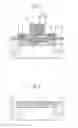
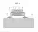
FIG. 7 is a cross-sectional view illustrating a semiconductor device according to a second embodiment of the present invention. FIG. 8 is a plan view illustrating an interior of the semiconductor device according to the second embodiment of the present invention. FIG. 9 is a cross-sectional view illustrating the semiconductor device in FIG. 7 mounted on a mounting substrate.
A semiconductor chip 11 is, for example, a transistor and a wiring structure provided on a semiconductor substrate. The semiconductor chip 11 is connected to leads 13 via wires 12. Parts of the semiconductor chip 11, the wires 12 and the leads 13 are covered with mold resin or the like, and a package 14 in which the semiconductor chip 11 is mounted is formed. An insulating film 15 covers an entire case of the package 14. The package 14 is mounted on a mounting substrate 16. In this case, the leads 13 are joined to electrodes 17 on the mounting substrate 16.
The insulating film 15 is formed using a method of laminating films of molecules of raw material compound by repeating steps of film formation through surface adsorption and reaction and removal of surplus molecules through purging for each monolayer, such as ALD. That is, a film whose principal ingredient is an oxide film on which atomic layers are alternately arrayed for each monolayer is used as the insulating film 15.
Although the package 14 mounted with the semiconductor chip 11 includes a large difference in height, the insulating film 15 of the present embodiment can cover all exposed portions of the case of the package 14 with a film of uniform thickness. Therefore, it is possible to prevent deterioration of moisture resistance of an FET or MMIC in the package 14 due to the high difference in height and insufficient film thickness in the rear portion.
Furthermore, the insulating film 15 is an insulating film whose principal ingredient is a Ta oxide film. Without being limited to this, however, the insulating film 15 may also be an insulating film whose principal ingredient is a Si oxide film or the insulating film 15 may be an insulating film whose principal ingredient is a layered structure of a Ta oxide film and a Si oxide film.
Obviously many modifications and variations of the present invention are possible in the light of the above teachings. It is therefore to be understood that within the scope of the appended claims the invention may be practiced otherwise than as specifically described.
The entire disclosure of Japanese Patent Application No. 2016-005382, filed on Jan. 14, 2016 including specification, claims, drawings and summary, on which the Convention priority of the present application is based, is incorporated herein by reference in its entirety.
Claims
1. A semiconductor device comprising:
a semiconductor substrate;
a semiconductor layer on the semiconductor substrate;
a source electrode and a drain electrode spaced apart from each other on the semiconductor layer;
a gate electrode on the semiconductor layer between the source electrode and the drain electrode; and
an insulating film covering the semiconductor layer, the source electrode, the drain electrode and the gate electrode,
the gate electrode has an eaves structure including a lower electrode joined to the semiconductor layer and an upper electrode provided on the lower electrode and wider than the lower electrode,
a principal ingredient of the insulating film is an oxide film where atomic layers are alternately arrayed for each monolayer, and
a film thickness of the insulating film that covers the lower electrode of the gate electrode is equal to a film thickness of the insulating film that covers the upper electrode.
2. The semiconductor device of claim 1, wherein a concave portion is formed in the semiconductor layer, and the lower electrode of the gate electrode is joined to a bottom surface of the concave portion
3. The semiconductor device of claim 1, wherein the principal ingredient of the insulating film is a Ta oxide film.
4. The semiconductor device of claim 1, wherein the principal ingredient of the insulating film is a Si oxide film.
5. The semiconductor device of claim 1, wherein the principal ingredient of the insulating film is a layered structure of a Ta oxide film and a Si oxide film.
6. A semiconductor device comprising:
a semiconductor chip;
a package in which the semiconductor chip is mounted; and
an insulating film covering the package,
wherein a principal ingredient of the insulating film is an oxide film where atomic layers are alternately arrayed for each monolayer.
7. The semiconductor device of claim 6, wherein the principal ingredient of the insulating film is a Ta oxide film.
8. The semiconductor device of claim 6, wherein the principal ingredient of the insulating film is a Si oxide film.
9. The semiconductor device of claim 6, wherein the principal ingredient of the insulating film is a layered structure of a Ta oxide film and a Si oxide film.
10. A manufacturing method of a semiconductor device comprising:
forming a semiconductor layer on a semiconductor substrate;
forming a source electrode and a drain electrode spaced apart from each other on the semiconductor layer;
forming a gate electrode on the semiconductor layer between the source electrode and the drain electrode; and
forming an insulating film covering the semiconductor layer, the source electrode, the drain electrode and the gate electrode,
the gate electrode has an eaves structure including a lower electrode joined to the semiconductor layer and an upper electrode provided on the lower electrode and wider than the lower electrode,
the insulating film is formed using a method of laminating films of molecules of raw material compound by repeating steps of film formation through surface adsorption and reaction and removal of surplus molecules through purging for each monolayer, and
a film thickness of the insulating film that covers the lower electrode of the gate electrode is equal to a film thickness of the insulating film that covers the upper electrode.
11. A manufacturing method of a semiconductor device comprising:
forming a package in which the semiconductor chip is mounted; and
forming an insulating film covering the package,
wherein the insulating film is formed using a method of laminating films of molecules of raw material compound by repeating steps of film formation through surface adsorption and reaction and removal of surplus molecules through purging for each monolayer.
Images & Drawings included:


Sources:
- United States Patent and Trademark Office - verify current appl. status at the USPTO↗
Similar patent applications:
- » 20110227139
Nonvolatile semiconductor memory device and manufacturing method thereof, semiconductor device and manufacturing method thereof, and manufacturing method of insulating film - » 20080290393
Nonvolatile semiconductor memory device and manufacturing method thereof, semiconductor device and manufacturing method thereof, and manufacturing method of insulating film - » 20090004846
Wiring board, manufacturing method thereof, semiconductor device and manufacturing method thereof - » 20090302457
Wiring substrate, manufacturing method thereof, semiconductor device, and manufacturing method thereof - » 20130056742
Microcrystalline silicon film, manufacturing method thereof, semiconductor device, and manufacturing method thereof - » 20120273034
METAL SUBSTRATE WITH INSULATION LAYER AND MANUFACTURING METHOD THEREOF, SEMICONDUCTOR DEVICE AND MANUFACTURING METHOD THEREOF, SOLAR CELL AND MANUFACTURING METHOD THEREOF, ELECTRONIC CIRCUIT AND MANUFACTURING METHOD THEREOF, AND LIGHT-EMITTING ELEMENT AND MANUFACTURING METHOD THEREOF - » 20050040531
Wiring board, manufacturing method thereof, semiconductor device and manufacturing method thereof - » 20070164306
III nitride semiconductor crystal and manufacturing method thereof, III nitride semiconductor device manufacturing method thereof, and light emitting device - » 20080303153
SEMICONDUCTOR DEVICE, MANUFACTURING METHOD THEREOF, AND SEMICONDUCTOR DEVICE PRODUCT - » 20100320445
Separation method of nitride semiconductor layer, semiconductor device, manufacturing method thereof, semiconductor wafer, and manufacturing method thereof
Recent applications in this class:
- » 20250174579 2025-05-29
SINGLE PIXEL MOISTURE PROTECTION (SPMP) - » 20250140713 2025-05-01
MOISTURE RESISTANT SEMICONDUTOR DEVICE - » 20250132269 2025-04-24
SEMICONDUCTOR DEVICE - » 20250112177 2025-04-03
SELF-ALIGNMENT ASSISTED ASSEMBLY ON A STRUCTURAL WAFER FOR HYBRID BONDED DIE STACKS - » 20250079341 2025-03-06
SEMICONDUCTOR STRUCTURE AND METHOD OF FORMING THE SAME - » 20250079340 2025-03-06
THROUGH WAFER TRENCH ISOLATION BETWEEN TRANSISTORS IN AN INTEGRATED CIRCUIT - » 20250079339 2025-03-06
SEMICONDUCTOR DEVICES WITH DUMMY FILL STRUCTURES BETWEEN A THROUGH SILICON VIA AND AN ACTIVE DEVICE AND METHODS OF FORMING THE SAME - » 20250070052 2025-02-27
SEMICONDUCTOR DEVICE WITH SEAL RING STRUCTURE AND METHOD FOR FORMING THE SAME - » 20250054879 2025-02-13
FORMING LARGE CHIPS THROUGH STITCHING - » 20250046734 2025-02-06
PACKAGE CONNECTORS IN SEMICONDCUTOR PACKAGES AND METHODS OF FORMING
Recent applications for this Assignee:
- » 20250176211 2025-05-29
SEMICONDUCTOR DEVICE AND METHOD OF MANUFACTURING SEMICONDUCTOR DEVICE - » 20250176196 2025-05-29
SEMICONDUCTOR DEVICE - » 20250175212 2025-05-29
COMMUNICATION DEVICE - » 20250175160 2025-05-29
NOISE FILTER - » 20250175128 2025-05-29
POWER AMPLIFIER - » 20250175049 2025-05-29
ARMATURE AND ELECTRIC MOTOR - » 20250173505 2025-05-29
INFORMATION PROCESSING SYSTEM, INFORMATION PROCESSING DEVICE, INFORMATION PROCESSING METHOD, AND RECORDING MEDIUM - » 20250173242 2025-05-29
LOG DATA ANALYSIS ASSISTANCE SYSTEM, LOG DATA ANALYSIS ASSISTANCE METHOD, RECORDING MEDIUM, AND ASSISTANCE DEVICE - » 20250173200 2025-05-29
CONTROL DEVICE, CONTROL METHOD, AND PROGRAM - » 20250173128 2025-05-29
RECORDING MEDIUM, PROGRAMMING ASSISTING DEVICE, AND PROGRAMMING ASSISTING METHOD