Display panel, fabricating method thereof, and display apparatus
US20170229526A1
2017-08-10
15/500,731
2016-06-07
✅ Patent granted
US 10,243,027 B2
2019-03-26
WO; PCT/CN2016/085096; 20160607
WO; WO2017/032131; 20170302
David Vu | Brandon Fox
Anova Law Group, PLLC
2036-06-15
Abstract:
In accordance with various embodiments of the disclosed subject matter, a display panel, a fabricating method thereof, and a related display apparatus are provided. In some embodiments, the display panel comprises: a base substrate comprising a display region and a peripheral region, wherein the peripheral region surrounds the display region; a light emitting device in the display region; a buffer layer on the peripheral region; and a first sealing layer on the buffer layer and the light emitting device.
Assignee:
- BOE TECHNOLOGY GROUP CO., LTD. 20,350 🇨🇳 Beijing, China
Applicant:
Interested in similar patents?
Get notified when new applications in this technology area are published.
Classification:
H01L27/3232 » CPC main
Devices consisting of a plurality of semiconductor or other solid-state components formed in or on a common substrate including components using organic materials as the active part, or using a combination of organic materials with other materials as the active part with components specially adapted for light emission, e.g. flat-panel displays using organic light-emitting diodes [OLED]; OLED integrated with another component the other component being a light modulating element, e.g. electrochromic element, photochromic element, liquid crystal element
H01L27/307 » CPC further
Devices consisting of a plurality of semiconductor or other solid-state components formed in or on a common substrate including components using organic materials as the active part, or using a combination of organic materials with other materials as the active part with components specially adapted for sensing infra-red radiation, light, electromagnetic radiation of shorter wavelength, or corpuscular radiation; with components specially adapted for either the conversion of the energy of such radiation into electrical energy or for the control of electrical energy by such radiation; Devices controlled by radiation Imager structures
H01L27/016 » CPC further
Devices consisting of a plurality of semiconductor or other solid-state components formed in or on a common substrate comprising only passive thin-film or thick-film elements formed on a common insulating substrate Thin-film circuits
H01L27/32 » CPC further
Devices consisting of a plurality of semiconductor or other solid-state components formed in or on a common substrate including components using organic materials as the active part, or using a combination of organic materials with other materials as the active part with components specially adapted for light emission, e.g. flat-panel displays using organic light-emitting diodes [OLED]
H01L27/30 IPC
Devices consisting of a plurality of semiconductor or other solid-state components formed in or on a common substrate including components using organic materials as the active part, or using a combination of organic materials with other materials as the active part with components specially adapted for sensing infra-red radiation, light, electromagnetic radiation of shorter wavelength, or corpuscular radiation; with components specially adapted for either the conversion of the energy of such radiation into electrical energy or for the control of electrical energy by such radiation
H01L27/12 » CPC further
Devices consisting of a plurality of semiconductor or other solid-state components formed in or on a common substrate including semiconductor components specially adapted for rectifying, oscillating, amplifying or switching and having at least one potential-jump barrier or surface barrier; including integrated passive circuit elements with at least one potential-jump barrier or surface barrier the substrate being other than a semiconductor body, e.g. an insulating body
H01L51/00 » CPC further
Solid state devices using organic materials as the active part, or using a combination of organic materials with other materials as the active part; Processes or apparatus specially adapted for the manufacture or treatment of such devices, or of parts thereof
H01L51/0097 » CPC further
Solid state devices using organic materials as the active part, or using a combination of organic materials with other materials as the active part; Processes or apparatus specially adapted for the manufacture or treatment of such devices, or of parts thereof; Substrates flexible substrates
H01L51/5237 » CPC further
Solid state devices using organic materials as the active part, or using a combination of organic materials with other materials as the active part; Processes or apparatus specially adapted for the manufacture or treatment of such devices, or of parts thereof specially adapted for light emission, e.g. organic light emitting diodes [OLED] or polymer light emitting devices [PLED]; Details of devices Passivation; Containers; Encapsulation, e.g. against humidity
H01L51/5253 » CPC further
Solid state devices using organic materials as the active part, or using a combination of organic materials with other materials as the active part; Processes or apparatus specially adapted for the manufacture or treatment of such devices, or of parts thereof specially adapted for light emission, e.g. organic light emitting diodes [OLED] or polymer light emitting devices [PLED]; Details of devices; Passivation; Containers; Encapsulation, e.g. against humidity Protective coatings
H01L51/5256 » CPC further
Solid state devices using organic materials as the active part, or using a combination of organic materials with other materials as the active part; Processes or apparatus specially adapted for the manufacture or treatment of such devices, or of parts thereof specially adapted for light emission, e.g. organic light emitting diodes [OLED] or polymer light emitting devices [PLED]; Details of devices; Passivation; Containers; Encapsulation, e.g. against humidity; Protective coatings having repetitive multilayer structures
H01L27/0262 » CPC further
Devices consisting of a plurality of semiconductor or other solid-state components formed in or on a common substrate including semiconductor components specially adapted for rectifying, oscillating, amplifying or switching and having at least one potential-jump barrier or surface barrier; including integrated passive circuit elements with at least one potential-jump barrier or surface barrier; Particular design considerations for integrated circuits for electrical or thermal protection, e.g. electrostatic discharge [ESD] protection for MOS devices using bipolar transistors as protective elements including a PNP transistor and a NPN transistor, wherein each of said transistors has its base coupled to the collector of the other transistor, e.g. silicon controlled rectifier [SCR] devices
H01L2251/5338 » CPC further
Indexing scheme relating to organic semiconductor devices covered by group; Organic light emitting devices; Structure Flexible OLED
H01L51/52 IPC
Solid state devices using organic materials as the active part, or using a combination of organic materials with other materials as the active part; Processes or apparatus specially adapted for the manufacture or treatment of such devices, or of parts thereof specially adapted for light emission, e.g. organic light emitting diodes [OLED] or polymer light emitting devices [PLED] Details of devices
H01L27/01 IPC
Devices consisting of a plurality of semiconductor or other solid-state components formed in or on a common substrate comprising only passive thin-film or thick-film elements formed on a common insulating substrate
H01L27/02 IPC
Devices consisting of a plurality of semiconductor or other solid-state components formed in or on a common substrate including semiconductor components specially adapted for rectifying, oscillating, amplifying or switching and having at least one potential-jump barrier or surface barrier; including integrated passive circuit elements with at least one potential-jump barrier or surface barrier
Description
CROSS-REFERENCES TO RELATED APPLICATIONS
This PCT patent application claims priority of Chinese Patent Application No. 201510536844.2, filed on Aug. 27, 2015, the entire content of which is incorporated by reference herein.
TECHNICAL FIELD
The disclosed subject matter generally relates to display technologies and, more particularly, relates to a display panel, a fabricating method thereof, and a related display apparatus.
BACKGROUND
A flexible display apparatus often includes a light emitting device formed on a flexible substrate, and a thin film encapsulation layer formed for protecting the light emitting device from external moisture and oxygen influences. Since there are many right-angle-corner regions on the edge of the flexible display apparatus, the thin film encapsulation layer may be cracked under stress when the flexible display apparatus is bent. This problem can result in a degradation in water resistance and oxygen resistance of the thin film encapsulation layer, thus affecting the life of the flexible display apparatus.
Accordingly, it is desirable to provide a display panel, a fabricating method thereof, and a related display apparatus to at least partially alleviate one or more problems set forth above and to solve other problems in the art.
BRIEF SUMMARY
In accordance with sonic embodiments of the disclosed subject matter, a display panel, a fabricating method thereof, and a related display apparatus are provided.
An aspect of the present disclosure provides a display panel, comprising: a base substrate comprising a display region and a peripheral region, wherein the peripheral region surrounds the display region; a light emitting device in the display region; a buffer layer on the peripheral region; and a first sealing layer on the buffer layer and the light emitting device.
In some embodiments, the display panel further comprises a planarization layer on the first sealing layer and a second sealing layer on the planarization layer.
In some embodiments, the buffer layer comprises at least one ring structure; and the at least one ring structure surrounds the display region.
In some embodiments, a thickness range of the buffer layer is 1 μm to 10 nm.
In some embodiments, the display panel further comprises: a first barrier wall in a first side of the peripheral region that is close to the display region, wherein the first barrier wall surrounds the display region.
In some embodiments, the display panel further comprises: a second barrier wall in a second side of the peripheral region that is far from the display region, wherein the second barrier wall surrounds the display region.
In some embodiments, the display panel further comprises: a rust barrier wall in a first side of the edge region that is close to the display region, wherein the first barrier wall surrounds the display region; and a second barrier wall in a second side of the edge region that is far from the display region, wherein the second barrier wall surrounds the display region.
In some embodiments, the first second barrier and the second barrier wall are linear line shaped, wavy line shaped, or fold line shaped.
In some embodiments, a material of the first second barrier or the second barrier wall comprises at least one of SiNx, SiO2, SiC, SiCN, SiCO polymer monomer, and hexamethyldisiloxane.
Another aspect of the present disclosure provides a display apparatus, comprising: a disclosed display panel; and a thin film transistor on the base substrate, wherein the light emitting device is on the thin film transistor.
In some embodiments, the base substrate is a flexible substrate; and the light emitting device is an organic light emitting diode.
In some embodiments, the buffer layer comprises a first ring structure and a second ring structure, wherein: the first ring structure surrounds the display region; the pixel defining layer surrounds the first ring structure; and the second ring structure surrounds the pixel defining layer.
Another aspect of the present disclosure provides a method for fabricating:
a display panel, comprising: forming a base substrate comprising a display region and a peripheral region, wherein the peripheral region surrounds the display region; forming a light emitting device in the display region; forming a buffer layer in the peripheral region; and forming a first sealing layer on the buffer layer and the light emitting device.
In some embodiments, the method for fabricating the display panel further comprises: forming a planarization layer on the first sealing layer; and forming a second sealing layer on the planarization layer.
In some embodiments, forming a buffer layer in the peripheral region further comprises: printing or coating a buffer layer film in the peripheral region; and forming the buffer layer by performing a patterning process on the buffer layer film.
In some embodiments, the method for fabricating the display panel further comprises: forming: a first barrier walls on a first side of the peripheral region that is close to the display region wherein the first barrier wall surrounds the display region.
In some embodiments, the method for fabricating the display panel further comprises: forming a second barrier walls on a second side of the peripheral region that is far from the display region, wherein the second barrier wall surrounds the display region.
In some embodiments, the method for fabricating the display panel further comprises: forming a first barrier walls on a first side of the edge region that is close to the display region, wherein the first barrier wall surrounds the display region; and forming a second barrier walls on a second side of the edge region that is far from the display region, wherein the second barrier wall surrounds the display region.
In some embodiments, the first second barrier and the second barrier wall are formed by using at least one material from SiNx, SiO2, SiC, SiCN, SiCO, polymer monomer, and hexamethyldisiloxane.
In some embodiments, forming a light emitting device in the display region further comprises: forming an organic light emitting diode in the display region of the base substrate, wherein the base substrate is a flexible substrate.
Other aspects of the present disclosure can be understood by those skilled in the art in light of the description, the claims, and the drawings of the present disclosure.
BRIEF DESCRIPTION OF THE DRAWINGS
Various objects, features, and advantages of the disclosed subject matter can be more fully appreciated with reference to the following detailed description of the disclosed subject matter when considered in connection with the following drawings, in which like reference numerals identify like elements. It should be noted that the following drawings are merely examples for illustrative purposes according to various disclosed embodiments and are not intended to limit the scope of the present disclosure.
FIG. 1 is a schematic sectional view diagram of a display panel in accordance with some embodiments of the disclosed subject matter;
FIG. 2 is a schematic top view diagram of the display panel illustrated in FIG. 1;
FIG. 3 is a schematic. sectional view diagram of a display panel in accordance with some other embodiments of the disclosed subject matter;
FIG. 4 is a schematic top view diagram of the display panel illustrated in FIG. 3; and
FIG. 5 is a flowchart of a method for fabricating a display panel in accordance with some other embodiments of the disclosed subject matter.
DETAILED DESCRIPTION
For those skilled in the art to better understand the technical solution of the disclosed subject matter, reference will now be made in detail to exemplary embodiments of the disclosed subject matter, which are illustrated in the accompanying drawings. Wherever possible, the same reference numbers will be used throughout the drawings to refer to the same or like parts.
In accordance with various embodiments, the disclosed subject matter provides a display panel, a fabricating method thereof, and a related display apparatus.
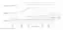
Referring to FIG. 1, a schematic sectional view diagram of a display panel is shown in accordance with some embodiments of the disclosed subject matter. The display panel comprises a thin film encapsulation structure used for encapsulating a light emitting device.
As illustrated, the thin film encapsulation structure can include a base substrate 101, a buffer layer 102, and a first sealing layer 103.
In some embodiments, the base substrate 101 includes a display region and a peripheral region. The peripheral region surrounds the display region.
A pixel defining layer 104 is disposed between the display region and the peripheral region. The light emitting device is disposed in the display region. The buffer layer 102 is disposed in the peripheral region. The first sealing layer 103 is disposed on the buffer layer 102 and the light emitting device.
Since the peripheral region includes many right-angle-corner structures, the peripheral region is not flat. The first sealing layer 103 includes one or more curved structures rather than right-angle-corner structures in the peripheral region. So the stress on the first sealing layer 103 in the peripheral region can be reduced to avoid cracking the first sealing layer 103 in the peripheral region caused by a too large stress. Therefore, the life of the display apparatus can be prolonged.
In some embodiments, the thin film encapsulation structure further includes a planarization layer 105 and a second sealing layer 106. The planarization layer 105 is disposed on the first sealing layer 103, the second sealing layer 106 is disposed on the planarization layer 105. Including a buffer layer, a planarization layer, and two sealing layers, the thin film encapsulation structure can have a better sealing function.
In some embodiments, the buffer layer 102 can have a thickness ranging from 1 μm to 10 μm. The material constituting the buffer layer 102 can include a polymer monomer material, a polyimide material or a polymethacrylate material.
As illustrated in FIG. 1, a thin film transistor array layer 107 is disposed on the base substrate 101. A cathode lead 108, the pixel defining layer 104, and an anode 109 of an organic light emitting diode are disposed on the thin film transistor array layer 107.
The pixel defining layer 104 includes two parts, one part is located outside of the cathode lead 108, the other part is located between the cathode lead 108 and the anode 109.
An organic light emitting layer 201 of the organic light emitting diode is disposed on the anode 109. A cathode 202 of the organic light emitting diode is disposed on the cathode lead 108, the pixel defining layer 104, and the organic light emitting layer 201. The cathode 202 is connected with drain electrode of thin film transistor through the cathode lead 108.
Referring to FIG. 2, a schematic top view diagram of the display panel illustrated in FIG. 1 is shown.
The buffer layer 102 includes at least one ring structure surrounding the display region. In some embodiments, the buffer layer 102 includes a first ring structure 203 and a second ring structure 204. Specifically, the first ring structure 203 surrounds the display region 205, the pixel defining layer 104 surrounds the first ring structure 203, the second ring structure 204 surrounds the pixel defining layer 104, and an epitaxial portion of the thin film transistor array layer 107 surrounds the second ring structure 204.
The disclosed display panel can comprises: a base substrate including a display region and a peripheral region, wherein the peripheral region surrounds the display region a light emitting device in the display region; a buffer layer on the peripheral region; and a first sealing layer on the buffer layer and the light emitting device. In the disclosed subject matter, the light emitting device is set in the display region, the buffer layer is set on the peripheral region, and the first sealing layer is set on the buffer layer and the light emitting device, so that the right-angle-corner structures on the first sealing layer in the peripheral region can be eliminated, thereby the stress on the first sealing layer in the peripheral region can be reduced to avoid cracking the first sealing layer in the peripheral region caused by a too large stress, and finally the life of the display apparatus can be prolonged.
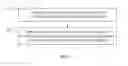
Referring, to FIG. 3, a schematic sectional view diagram of a display panel is shown in accordance with some other embodiments of the disclosed subject matter. The display panel comprises a thin film encapsulation structure used for encapsulating a light emitting device.
As illustrated, the thin film encapsulation structure can include a base substrate 101, a buffer layer 102, and a first sealing layer 103.
In some embodiments, the base substrate 101 includes a display region and a peripheral region. The peripheral region surrounds the display region.
A pixel defining layer 104 is disposed between the display region and the peripheral region. The light emitting device is disposed in the display region. The buffer layer 102 is disposed in the peripheral region. The first sealing layer 103 is disposed on the buffer layer 102 and the light emitting device.
Since the peripheral region includes many right-angle-corner structures, the peripheral region is not flat. The first sealing layer 103 includes one or more curved structures rather than right-angle-corner structures in the peripheral region. So the stress on the first sealing layer 103 in the peripheral region can be reduced to avoid cracking the first sealing layer 103 in the peripheral region caused by a too large stress. Therefore, the life of the display apparatus can be prolonged.
In some embodiments, the thin film encapsulation structure further includes a first barrier wall 206. The first barrier wall 206 is disposed in one side of the peripheral region that is close to the display region. The first barrier wall 206 surrounds the display region.
In some embodiments, the thin film encapsulation structure further includes a second barrier wall 207. The second barrier wall 207 is disposed in another side of the peripheral region that is far from the display region. The second barrier wall 207 surrounds the display region.
In some embodiments, the thin film encapsulation structure can include both the first barrier wall 206 and the second barrier wall 207. The first barrier wall 206 and the second barrier wall 207 can be used for preventing an overflowing of the material of the buffer layer 102, and thereby protecting the narrow border.
In some embodiments, the first barrier walls 206 and the second barrier wall 207 can have any suitable shape, such as linear line shape, wavy line shape, fold line shape, etc. The first barrier walls 206 and the second barrier wall 207 can be constituted by any suitable material, such as SiNx, SiO2, SiC, SiCN, SiCO, polymer monomer, Hexamethyldisiloxane (HMDSO), or one or more combinations thereof.
As illustrated in FIG. 3, a thin film transistor array layer 107 is disposed on the base substrate 101. A cathode lead 108, the pixel defining layer 104, and an anode 109 of an organic light emitting diode are disposed on the thin film transistor array layer 107.
The pixel defining layer 104 includes two parts, one part is located outside of the cathode lead 108, the other part is located between the cathode lead 108 and the anode 109.
An organic light emitting layer 201 of the organic light emitting diode is disposed on the anode 109. A cathode 202 of the organic, light emitting diode is disposed on the cathode lead 108, the pixel defining layer 104, and the organic light emitting layer 201.
The cathode 202 is connected with drain electrode of thin film transistor through the cathode lead 108.
Referring to FIG. 4, a schematic top view diagram of the display panel illustrated in FIG. 3 is shown.
The buffer layer 102 includes at least one ring structure surrounding the display region. In some embodiments, the buffer layer 102 includes a first ring structure 203 and a second ring structure 204. Specifically, the first barrier wall 206 surrounds the display region 205, the first ring structure 203 surrounds the first barrier wall 206, the pixel defining layer 104 surrounds the first ring structure 203, the second ring structure 204 surrounds the pixel defining layer 104, the second barrier wall 207 surrounds the second ring structure 204, and an epitaxial portion of the thin film transistor array layer 107 surrounds the second barrier wall 207.
The disclosed display panel can comprises: a base substrate including a display region and a peripheral region, wherein the peripheral region surrounds the display region; a light emitting device in the display region; a butler layer on the peripheral region; and a first sealing layer on the buffer layer and the tight emitting. device. In the disclosed subject matter, the light emitting device is set in the display region, the buffer layer is set on the peripheral region, and the first sealing layer is set on the buffer layer and the light emitting device, so that the right-angle-corner structures on the first sealing layer in the peripheral region can be eliminated, thereby the stress on the first sealing layer in the peripheral region can be reduced to avoid cracking the first sealing layer in the peripheral region caused by a too large stress, and finally the life of the display apparatus can be prolonged.
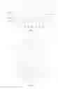
Referring to FIG. 5, a flowchart of a method for fabricating a display panel is shown in accordance with sonic other embodiments of the disclosed subject matter. The display panel comprises a thin film encapsulation structure used for encapsulating a light emitting device.
The display panel can include a base substrate including a display region and a peripheral region. The peripheral region surrounds the display region. The light emitting device is disposed in the display region.
As illustrated, the method can include:
Step S1: forming a buffer layer in the peripheral region.
In some embodiments, step S1 can include: printing or coating a buffer layer film in the peripheral region, and forming the buffer layer by performing a patterning process on the buffer layer film.
In some embodiments, prior to the step SI, the method can include forming one or more barrier walls in the edge area. The one or more barrier walls can surround the display region.
For example, a first barrier wall can be formed on one side of the peripheral region that is close to the display region. The first barrier wall surrounds the display region.
As another example, a second barrier wall can be formed on another side of the peripheral region that is fin from the display region. The second barrier wall surrounds the display region.
In some embodiments, the first barrier wall and the second barrier wall can both be formed. The first barrier wall and the second barrier wall are used for preventing an overflowing of the material of the buffer layer, and thereby protecting the narrow border.
Step S2: forming a first sealing layer on the buffer layer and the light emitting device.
Since the peripheral region includes many right-angle-comer structures, the peripheral region is not flat. The first sealing layer includes one or more curved structures rather than right-angle-comer structures in the peripheral region, So the stress on the first sealing layer 103 in the peripheral region can be reduced to avoid cracking the first sealing layer in the peripheral region caused by a too large stress. Therefore, the life of the display apparatus can be prolonged.
In some embodiments, the method further includes forming a planarization layer on the first sealing layer, and forming a second sealing, layer on the, planarization layer. Including a buffer layer, a planarization layer and two sealing layers, the thin film encapsulation structure can have a better sealing function.
Specifically, a thin film transistor array layer can be formed on the base substrate. A cathode lead, a pixel defining layer, and an anode of an organic light emitting diode can be formed on the thin film transistor array layer.
The pixel defining layer can include two parts, one part is located outside of the cathode lead, the other part is located between the cathode lead and the anode.
An organic light emitting layer of the organic light emitting diode can be formed on the anode. A cathode of the organic light emitting diode can be formed on the cathode lead, the pixel defining: layer, and the organic light emitting layer. The cathode can be connected with the drain electrode of thin film transistor through the cathode lead.
In the disclosed method for forming a display panel, the display panel can comprises: a base substrate including a display region and a peripheral region, wherein the peripheral region surrounds the display region; a light emitting device in the display region; a buffer layer on the peripheral region; and a first sealing layer on the buffer layer and the light emitting device. In the disclosed subject matter, the light emitting device is set in the display region, the buffer layer is set on the peripheral region, and the first sealing layer is set on the buffer layer and the light emitting device, so that the right-angle-corner structures on the first sealing layer in the peripheral region can be eliminated. thereby the stress on the first sealing layer in the peripheral region can be reduced to avoid cracking the first sealing layer in the peripheral region caused by a too large stress, and finally the life of the display apparatus can be prolonged.
Another aspect of the disclosed subject matter provides a display apparatus, including a thin film transistor, a light emitting device, and any one of the display panel described above.
In some embodiments, the thin film transistor is disposed on a base substrate, and the light emitting device is disposed on the thin film transistor.
The disclosed display apparatus includes a display panel comprising: a base substrate including a display region and a peripheral region, wherein the peripheral region surrounds the display region; a light emitting device in the display region; a buffer layer on the peripheral region; and first sealing layer on the buffer layer and the light emitting device. In the disclosed subject matter, the light emitting device is set in the display region, the buffer layer is set on the peripheral region, and the first sealing layer is set on the buffer layer and the light emitting device, so that the right-angle-corner structures on the first sealing layer in the peripheral region can be eliminated, thereby the stress on the first sealing layer in the peripheral region can be reduced to avoid cracking the first sealing layer in the peripheral region caused by a too large stress, and finally the life of the display apparatus can be prolonged.
The display apparatus can be any suitable device or component that has a display function, such as a LCD panel, an electronic paper, a mobile phone, a tablet computer, a television, a monitor, a notebook computer, a digital picture frame, a navigation system, a smart watch, etc.
The provision of the examples described herein (as well as clauses phrased as “such as,” “e.g.,” “including,” and the like) should not be interpreted as limiting the claimed subject matter to the specific examples; rather, the examples are intended to illustrate only some of many possible aspects.
Accordingly, a display panel, a fabricating method thereof, and a related display apparatus are provided.
Although the disclosed subject matter has been described and illustrated in the foregoing illustrative embodiments, it is understood that the present disclosure has been made only by way of example, and that numerous changes in the details of embodiment of the disclosed subject matter can be made without departing from the spirit and scope of the disclosed subject matter, which is only limited by the claims which follow. Features of the disclosed embodiments can be combined and rearranged in various ways. Without departing from the spirit and scope of the disclosed subject matter, modifications, equivalents, or improvements to the disclosed subject matter are understandable to those skilled in the art and are intended to be encompassed within the scope of the present disclosure.
Claims
1-20. (canceled)
21. A display panel, comprising:
a base substrate comprising a display region and a peripheral region, wherein the peripheral region surrounds the display region;
a light emitting device in the display region;
a buffer layer on the peripheral region; and
a first sealing layer on the buffer layer and the light emitting device.
22. The display panel of claim 21, further comprising:
a planarization layer on the first sealing layer; and
a second scaling layer on the planarization layer.
23. The display panel of claim 21, wherein:
the buffer layer comprises at least one ring structure; and
the at least one ring structure surrounds the display region.
24. The display panel of claim 21, wherein:
a thickness range of the buffer layer is 1 μm to 10 μm.
25. The display panel of claim 21, further comprising:
a first barrier wall in a first side of the peripheral region that is close to the display region, wherein the first barrier wall surrounds the display region.
26. The display panel of claim 21, further comprising:
a second barrier wall in a second side of the peripheral region that is far from the display region, wherein the second barrier wall surrounds the display region.
27. The display panel of claim 21, further comprising:
a first barrier wall in a first side of the edge region that is close to the display region, wherein the first barrier wail surrounds the display region; and
a second barrier wall in a second side of the edge region that is far from the display region, wherein the second barrier wall surrounds the display region.
28. The display of claim 27, wherein:
the first second barrier and the second barrier wall are linear line shaped, wavy line shaped, or fold line shaped.
29. The display panel of claim 27, wherein:
a material of the first second barrier or the second barrier wall comprises at least one of SiNx, SiO2, SIC, SiCN, SiCO, polymer monomer, and hexamethyldisiloxane.
30. A display apparatus, comprising:
a display panel of claim 21; and
a thin film transistor on the base substrate,
wherein the light emitting device is on the thin film transistor,
31. The display apparatus of claim 30, wherein:
the base substrate is a flexible substrate; and
the light emitting device is an organic light emitting diode.
32. The display apparatus of claim 31, wherein:
the buffer layer comprises a first ring structure and a second ring structure, wherein:
the first ring structure surrounds the display region;
the pixel defining layer surrounds the first ring structure; and
the second ring structure surrounds the pixel defining layer.
33. A method for fabricating a display panel, comprising:
forming a base substrate comprising a display region and a peripheral region, wherein the peripheral region surrounds the display region;
forming a light emitting device in the display region;
forming a buffer layer in the peripheral region; and
forming a first sealing layer on the buffer layer and the light emitting device.
34. The method for fabricating the display panel of claim 33, further comprising:
forming a planarization layer on the first sealing layer; and
forming a second sealing layer on the planarization layer.
35. The method for fabricating the display panel of claim 33, wherein forming a butler layer in the peripheral region further comprises:
printing or coating a buffer layer film in the peripheral region; and
forming the buffer layer by performing a patterning process on the buffer layer film.
36. The method for fabricating the display panel of claim 33, further comprising:
forming a first barrier walls on a first side of the peripheral region that is close to the display region, wherein the first barrier wall surrounds the display region.
37. The method for fabricating the display panel of claim 33, further comprising:
forming a second barrier walls on a second side of the peripheral region that is far from the display region, wherein the second barrier wall surrounds the display region.
38. The method for fabricating a display panel of claim 33, further comprising:
forming a first barrier walls on a first side of the edge region that is close to the display region, wherein, the first barrier wall surrounds the display region; and
forming a second barrier walls on a second side of the edge region that is far from the display region, wherein the second barrier wall surrounds the display region.
39. The method for fabricating the display panel of claim 38, wherein, the first second barrier and the second barrier wall are formed by using at least one material from SiNx, SiO2, SiC, SiCN SiCO, polymer monomer, and hexamethyldisoxane.
40. The method for fabricating the display panel of claim 33, wherein forming a light emitting device in the display region further comprises:
forming an organic light emitting diode in the display region of the base substrate,
wherein the base substrate is a flexible substrate.
Images & Drawings included:
Sources:
- United States Patent and Trademark Office - verify current appl. status at the USPTO↗
Similar patent applications:
- » 20210376030
Organic light-emitting diode apparatus with color film shielding layer, fabrication method thereof, display panel, and display apparatus - » 20180307074
Touch substrate, display panel, display apparatus, and fabricating method thereof - » 20150331231
Electrowetting display panel, fabrication method thereof and display apparatus comprising the same - » 20180019265
Display panel, fabrication method thereof and display apparatus - » 20170186995
Display substrate having driving wires and fabrication method thereof, display panel and display apparatus - » 20180212001
PIXEL STRUCTURE, FABRICATION METHOD THEREOF, DISPLAY PANEL, AND DISPLAY APPARATUS - » 20170294454
ARRAY SUBSTRATE AND FABRICATING METHOD THEREOF, DISPLAY PANEL, AND DISPLAY APPARATUS - » 20160358979
OLED UNIT AND FABRICATION METHOD THEREOF, DISPLAY PANEL AND DISPLAY APPARATUS - » 20160064415
Array substrate and fabricating method thereof, display panel and display apparatus - » 20180138252
Organic light-emitting display panel, fabrication method thereof, and display apparatus
Recent applications in this class:
- » 20240114744 2024-04-04
DISPLAY PANEL AND DISPLAY DEVICE - » 20230284506 2023-09-07
SWITCHABLE TRANSPARENT ORGANIC LIGHT-EMITTING DIODE DISPLAYS WITH AN INTEGRATED ELECTRONIC INK LAYER - » 20230217782 2023-07-06
VIEWING ANGLE CONTROL FILM AND DISPLAY DEVICE COMPRISING THE SAME - » 20230180575 2023-06-08
Display device - » 20230172028 2023-06-01
Display panel and electronic device including the same - » 20230057260 2023-02-23
SYSTEM AND METHOD FOR CONSTRUCTING AN ORGANIC LIGHT EMITTING DIODE (OLED) DISPLAY FOR OUTDOOR USE - » 20220406857 2022-12-22
Display substrate, display apparatus, and display substrate manufacture method - » 20220384537 2022-12-01
DISPLAY SUBSTRATE AND PREPARATION METHOD THEREFOR, AND DISPLAY APPARATUS - » 20220293698 2022-09-15
Display panel and display device - » 20220271105 2022-08-25
Display substrate, method of forming display substrate and display device
Recent applications for this Assignee:
- » 20250295022 2025-09-18
QUANTUM DOT COMPOSITION, LIGHT-EMITTING ELEMENT, DISPLAY PANEL AND PREPARATION METHOD THEREOF - » 20250295019 2025-09-18
HEAT DISSIPATION FILM, DISPLAY MODULE AND DISPLAY DEVICE - » 20250294987 2025-09-18
DISPLAY PANEL, DISPLAY DEVICE - » 20250294983 2025-09-18
DISPLAY PANEL AND DISPLAY DEVICE - » 20250292736 2025-09-18
DRIVING CIRCUIT, DRIVING METHOD, DRIVING MODULE AND DISPLAY DEVICE - » 20250291336 2025-09-18
COMPUTER-IMPLEMENTED METHOD, APPARATUS FOR MANAGING PRODUCTION OF ONE OR MORE PRODUCTS, AND COMPUTER-PROGRAM PRODUCT - » 20250291215 2025-09-18
CIRCUIT BOARD AND METHOD FOR MANUFACTURING THE SAME, LIGHT-EMITTING SUBSTRATE, BACKLIGHT MODULE, DISPLAY PANEL AND DISPLAY APPARATUS - » 20250287801 2025-09-11
ARRAY SUBSTRATE AND DISPLAY APPARATUS - » 20250287695 2025-09-11
ARRAY PANEL, METHOD OF MANUFACTURING THE SAME AND DISPLAY DEVICE - » 20250285597 2025-09-11
DISPLAY SUBSTRATE AND DISPLAY DEVICE