Power conversion apparatus
US20170272002A1
2017-09-21
15/422,448
2017-02-01
✅ Patent granted
US 10,381,947 B2
2019-08-13
-
-
Nguyen Tran | Bryan R Perez
Rabin & Berdo, P.C.
2037-03-11
Abstract:
A power conversion apparatus includes: a power module that converts an input of alternating current power into direct current (DC) power and outputs the DC power; and a gate driver unit that includes a first substrate having mounted thereon a gate driver circuit component that isolates a control signal input from a control apparatus, that converts the isolated control signal into a gate signal for driving the power module, and that outputs the gate signal, a second substrate that includes a wiring conductor fixed to a gate control terminal of the power module, and a connection member that includes a connector that connects the first substrate and the second substrate to each other.
Assignee:
- FUJI ELECTRIC CO., LTD. 2,338 🇯🇵 Kawasaki-shi, Japan
- FUJI ELECTRIC CO., LTD. 489 🇯🇵 Kawasaki-shi, Kanagawa, Japan
Applicant:
Interested in similar patents?
Get notified when new applications in this technology area are published.
Classification:
H02M1/08 » CPC further
Details of apparatus for conversion Circuits specially adapted for the generation of control voltages for semiconductor devices incorporated in static converters
H02M7/00 IPC
Conversion of ac power input into dc power output; Conversion of dc power input into ac power output
H02M7/003 » CPC further
Conversion of ac power input into dc power output; Conversion of dc power input into ac power output Constructional details, e.g. physical layout, assembly, wiring or busbar connections
H01L27/0629 » CPC further
Devices consisting of a plurality of semiconductor or other solid-state components formed in or on a common substrate including semiconductor components specially adapted for rectifying, oscillating, amplifying or switching and having at least one potential-jump barrier or surface barrier; including integrated passive circuit elements with at least one potential-jump barrier or surface barrier the substrate being a semiconductor body including a plurality of individual components in a non-repetitive configuration integrated circuits having a two-dimensional layout of components without a common active region comprising components of the field-effect type in combination with diodes, or resistors, or capacitors
H01L29/1608 » CPC further
Semiconductor devices adapted for rectifying, amplifying, oscillating or switching, or capacitors or resistors with at least one potential-jump barrier or surface barrier, e.g. PN junction depletion layer or carrier concentration layer; Details of semiconductor bodies or of electrodes thereof; Multistep manufacturing processes therefor; Semiconductor bodies ; Multistep manufacturing processes therefor characterised by the materials of which they are formed including, apart from doping materials or other impurities, only elements of Group IV of the Periodic System Silicon carbide
H01R12/52 » CPC further
Structural associations of a plurality of mutually-insulated electrical connecting elements, specially adapted for printed circuits, e.g. printed circuit boards [PCBs], flat or ribbon cables, or like generally planar structures, e.g. terminal strips, terminal blocks; Coupling devices specially adapted for printed circuits, flat or ribbon cables, or like generally planar structures; Terminals specially adapted for contact with, or insertion into, printed circuits, flat or ribbon cables, or like generally planar structures; Fixed connections for rigid printed circuits or like structures connecting to other rigid printed circuits or like structures
H05K7/1427 » CPC further
Constructional details common to different types of electric apparatus; Mounting supporting structure in casing or on frame or rack; Printed circuit boards receptacles, e.g. stacked structures, electronic circuit modules or box like frames Housings
H05K7/1427 » CPC further
Constructional details common to different types of electric apparatus; Mounting supporting structure in casing or on frame or rack; Printed circuit boards receptacles, e.g. stacked structures, electronic circuit modules or box like frames Housings
H05K7/1432 » CPC further
Constructional details common to different types of electric apparatus; Mounting supporting structure in casing or on frame or rack; Printed circuit boards receptacles, e.g. stacked structures, electronic circuit modules or box like frames; Housings specially adapted for power drive units or power converters
H02M7/217 » CPC main
Conversion of ac power input into dc power output; Conversion of dc power input into ac power output; Conversion of ac power input into dc power output without possibility of reversal by static converters using discharge tubes with control electrode or semiconductor devices with control electrode using devices of a triode or transistor type requiring continuous application of a control signal using semiconductor devices only
H01L29/872 » CPC further
Semiconductor devices adapted for rectifying, amplifying, oscillating or switching, or capacitors or resistors with at least one potential-jump barrier or surface barrier, e.g. PN junction depletion layer or carrier concentration layer; Details of semiconductor bodies or of electrodes thereof; Multistep manufacturing processes therefor; Types of semiconductor device ; Multistep manufacturing processes therefor controllable only by variation of the electric current supplied, or only the electric potential applied, to one or more of the electrodes carrying the current to be rectified, amplified, oscillated or switched; Diodes Schottky diodes
H05K7/14 IPC
Constructional details common to different types of electric apparatus Mounting supporting structure in casing or on frame or rack
H05K7/14 IPC
Constructional details common to different types of electric apparatus Mounting supporting structure in casing or on frame or rack
H01L27/06 IPC
Devices consisting of a plurality of semiconductor or other solid-state components formed in or on a common substrate including semiconductor components specially adapted for rectifying, oscillating, amplifying or switching and having at least one potential-jump barrier or surface barrier; including integrated passive circuit elements with at least one potential-jump barrier or surface barrier the substrate being a semiconductor body including a plurality of individual components in a non-repetitive configuration
H01L29/16 IPC
Semiconductor devices adapted for rectifying, amplifying, oscillating or switching, or capacitors or resistors with at least one potential-jump barrier or surface barrier, e.g. PN junction depletion layer or carrier concentration layer; Details of semiconductor bodies or of electrodes thereof; Multistep manufacturing processes therefor; Semiconductor bodies ; Multistep manufacturing processes therefor characterised by the materials of which they are formed including, apart from doping materials or other impurities, only elements of Group IV of the Periodic System
Description
CROSS-REFERENCE TO RELATED APPLICATION
This application is based upon and claims the benefit of priority of the prior Japanese Patent Application No. 2016-051938, filed on Mar. 16, 2016, the entire contents of which are incorporated herein by reference.
BACKGROUND OF THE INVENTION
Technical Field
The present invention relates to a power conversion apparatus.
Background Art
A power conversion apparatus that converts input AC (Alternating Current) power into DC (Direct Current) power and that outputs the DC power includes a gate driver unit and a power module.
The gate driver unit (GDU) includes a gate substrate. The gate substrate has mounted thereon a gate driver circuit component for isolating a control signal input from a control apparatus outside the power conversion apparatus, for converting the isolated control signal into a gate signal, and for outputting the gate signal.
The power module includes, for example, a switching element and a freewheeling diode connected in inverse-parallel to the switching element. The switching element is turned on or off in accordance with a gate signal input from the gate driver unit via a gate control line. The freewheeling diode causes a current generated upon turning on the switching element to detour around the switching element so as to prevent a failure of the switching element.
The gate driver circuit component includes a gate resistor. The gate resistor is connected to a gate control line between the gate driver unit and the switching element. The gate resistor suppresses a surge voltage generated upon turning off the switching element or noise generated upon switching so as to stabilize a gate signal input to the switching element.
Recently, wide bandgap semiconductors have been sometimes used for switching elements in power modules. An exemplary wide bandgap semiconductor is a SiC (silicon carbide)-MOSFET (Metal-Oxide-Semiconductor Field-Effect Transistor). In comparison with a Si (Silicon)-based switching element such as a Si-IGBT (Insulated Gate Bipolar Transistor), a wide bandgap semiconductor may have pressure resistance and achieve fast switching. To enable fast switching of a switching element comprising such a wide bandgap semiconductor, a gate resistor needs to be operated effectively. Hence, the gate electrode is desirably located near the switching element.
A gate driver unit described in Japanese Laid-open Patent Publication No. 2015-198545 includes a first substrate (gate substrate) and a second substrate (gate relay substrate) that is fixed to a gate terminal of a power module by soldering or the like. A gate resistor is mounted on the second substrate. The second substrate is connected to the first substrate by a gate control line. The gate control line is fixed to the first and second substrates by soldering or the like. A well-known example of the gate control line is a wiring conductor plate wherein a gate wire and a source wire (ground wire) form a laminated structure with an insulation sheet interposed therebetween so as to decrease the wiring inductance of a gate circuit.
The gate driver circuit component and the power module may be expensive. Hence, when one of the gate driver circuit component or the power module has failed, it is desirable to replace only the faulty one. However, when the gate substrate having the gate driver circuit component mounted thereon and the gate relay substrate fixed to the power module have been fixed to the gate control line, the gate driver circuit component and the power module cannot be readily separated from each other. Thus, even when only one of the gate driver circuit component or the power module has failed, not only the faulty one but also the other one, i.e., the normal one, needs to be replaced, thereby leading to a high repair cost.
SUMMARY OF THE INVENTION
A power conversion apparatus in accordance with an embodiment includes a power module and a gate driver unit. The power module converts input AC power into DC power and outputs the DC power. The gate driver unit includes a first substrate, a second substrate, and a connection member. The first substrate has mounted thereon a gate driver circuit component that isolates a control signal input from a control apparatus, that converts the isolated control signal into a gate signal for driving the power module, and that outputs the gate signal. The second substrate includes a wiring conductor fixed to a gate control terminal of the power module. The connection member includes a connector that connects the first and second substrates to each other.
BRIEF DESCRIPTION OF THE DRAWINGS
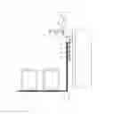
FIG. 1 is a schematic side view illustrating an example of a power conversion apparatus in accordance with an embodiment;
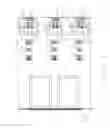
FIG. 2 is a schematic top view illustrating an example of a power conversion apparatus in accordance with an embodiment;
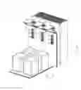
FIG. 3 is a schematic perspective view illustrating an example of a power conversion apparatus in accordance with an embodiment;
FIG. 4 is a side view illustrating the power conversion apparatus depicted in FIG. 1 with a capacitor and a bus bar removed therefrom;
FIG. 5 is a top view illustrating the power conversion apparatus depicted in FIG. 2 with a capacitor and a bus bar removed therefrom;
FIG. 6 is a perspective view illustrating the power conversion apparatus depicted in FIG. 3 with a capacitor and a bus bar removed therefrom;
FIG. 7 illustrates an example of the arrangement of power modules in a power conversion apparatus in accordance with an embodiment; and
FIG. 8 illustrates another example of a connection member of a power conversion apparatus in accordance with an embodiment.
DETAILED DESCRIPTION OF EMBODIMENTS
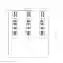
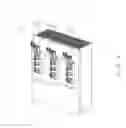
The following describes modes for carrying out the present invention by referring to the drawings. FIG. 1 is a schematic side view illustrating an example of a power conversion apparatus in accordance with an embodiment. FIG. 2 is a schematic top view illustrating an example of a power conversion apparatus in accordance with an embodiment. FIG. 3 is a schematic perspective view illustrating an example of a power conversion apparatus in accordance with an embodiment. In the drawings, like reference numerals refer to like parts. In the example depicted in FIGS. 1-3, a power conversion apparatus 1 includes power modules 2, gate driver units 3, a cooler 4, and capacitors 5.
The power module 2 converts input AC power into DC power and outputs the DC power. The power module 2 may include a switching element and a freewheeling diode connected in inverse-parallel to the switching element. The switching element included in the power module 2 may be a wide bandgap semiconductor, e.g., a SiC-MOSFET. The freewheeling diode included in the power module 2 may be, for example, a SiC Schottky barrier diode.
In the exemplary configuration depicted in FIGS. 1-3, three power modules 2 each convert a corresponding one of the three phases of AC power into DC power and each output the resultant DC power. Each power module 2 may be a 2-in-1 power module having a set corresponding to an upper arm and a set corresponding to a lower arm connected in series to each other, each set comprising a switching element and a freewheeling diode.
The power module 2 is disposed on the cooler 4, and a bottom surface of the power module 2 faces a top surface of the cooler 4. A gate control terminal 21, a source control terminal 22, a high-potential main terminal 23, a ground main terminal 24, and an output terminal 25 are disposed on a top surface of the power module 2. For example, the gate control terminal 21 may be a control terminal connected to a gate of each switching element, and the source control terminal 22 may be a control terminal connected to a source of each switching element. The high-potential main terminal 23 is a main terminal connected to a drain of a switching element of the upper arm, and the ground main terminal 24 is a main terminal connected to a source of a switching element of the lower arm. The output terminal 25 is a main terminal connected to the source of the switching element of the upper arm and to the drain of the switching element of the lower arm.
The high-potential main terminal 23 and the ground main terminal 24 are connected to the capacitor 5 via a bus bar 6. As depicted in FIGS. 1-3, the bus bar 6 may include a first surface 61 and a second surface 62. The first surface 61 may be parallel to the top surface of the power module 2. The high-potential main terminal 23 and the ground main terminal 24 are each connected to a corresponding wiring conductor within the first surface 61. The second surface 62 may be located at a position higher than the power module 2 and may be perpendicular to the top surface of the power module 2. Each terminal of the capacitor 5 is connected to a corresponding wiring conductor within the second surface 62.
The capacitor 5 is a smoothing capacitor that attenuates a ripple current generated due to a switching operation of a switching element. Although FIGS. 1-3 depict four capacitors 5, the power conversion apparatus in accordance with the embodiment may include an arbitrary number of capacitors.
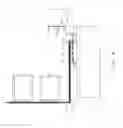
The gate driver unit 3 includes a first substrate 31, a second substrate 32, and a connection member 33.
The first substrate 31 corresponds to a gate substrate and has a gate driver circuit component 311 mounted thereon. The gate driver circuit component 311 isolates a control signal input from a control circuit (not illustrated) connected via a connection terminal 312, converts the isolated control signal into a gate signal for driving the power module 2, and outputs the resultant signal. The control signal input from the control circuit may be a PWM (Pulse Width Modulation) signal.
The second substrate 32 is disposed on the power module 2 so as to cover a portion of the top surface of the power module 2. The second substrate 32 corresponds to the gate relay substrate. The gate control terminal 21 and the source control terminal 22 are each connected to a corresponding wiring conductor within the second substrate 32 by soldering or the like. The second substrate 32 may have a gate resistor 321 mounted thereon. The second substrate 32 having the gate resistor 321 mounted thereon allows the gate resistor 321 to be located close to a switching element included in the power module 2. Hence, the gate resistor can be effectively operated even when the switching element is fast switched using a wide bandgap semiconductor.
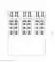
When a plurality of power modules 2 are arranged in parallel as depicted in FIGS. 4-6, W1 may be equal to or less than W2, where W1 represents the parallel-direction width of each of a plurality of second substrates 32 arranged in parallel in association with the plurality of power modules 2, and W2 represents the parallel-direction width of an associated power module 2. FIG. 4 is a side view illustrating the power conversion apparatus depicted in FIG. 1 with the capacitor and the bus bar removed therefrom. FIG. 5 is a top view illustrating the power conversion apparatus depicted in FIG. 2 with the capacitor and the bus bar removed therefrom. FIG. 6 is a perspective view illustrating the power conversion apparatus depicted in FIG. 3 with the capacitor and the bus bar removed therefrom. The second substrates 32 having the size as described above allows an area on which are mounted the plurality of parallely arranged power modules 2 to be suppressed. When, for example, two power module groups each including the three power modules 2 depicted in FIGS. 1-5 are mounted on the power conversion apparatus 1, as illustrated in FIG. 7, an area on which are mounted six parallely arranged power modules 2 can be suppressed. FIG. 7 illustrates an example of the arrangement of power modules in the power conversion apparatus in accordance with an embodiment.
The connection member 33 includes a connector 331 that connects the first substrate 31 and the second substrate 32.
As described above, a well-known gate control line between the first substrate 31 and the second substrate 32 is, for example, a wiring conductor plate wherein a gate wire and a source wire (ground wire) form a laminated structure with an insulation sheet interposed therebetween so as to decrease the wiring inductance. Connecting a connector to such a wiring conductor plate and then connecting the wiring conductor plate to the first substrate 31 and the second substrate 32 via the connector would less effectively decrease the wiring inductance. Hence, it would be desirable to connect the wiring conductor plate directly to terminals (pins) of the first substrate 31 and the second substrate 32 by soldering or the like. However, if the wiring conductor plate is fixed to terminals of the first substrate 31 and the second substrate 32 by soldering or the like, the first substrate 31 having the gate driver circuit component 311 mounted thereon and the power module 2 having the second substrate 32 fixed thereto would not be readily separated from each other after the first substrate 31 and the power module 2 have been implemented on the power conversion apparatus 1.
By contrast, in the power conversion apparatus 1, the first substrate 31 having the gate driver circuit component 311 mounted thereon and the second substrate 32 fixed to the power module 2 are connected to each other using the connector 331 included in the connection member 33. Hence, in the power conversion apparatus in accordance with the embodiment, the first substrate 31 having the gate driver circuit component 311 mounted thereon and the power module 2 having the second substrate 32 fixed thereto can be readily separated from each other after the first substrate 31 and the power module 2 have been implemented on the power conversion apparatus. The connection member 33 that includes the connector 331 also has the advantage that the connection member 33 can be manufactured at a lower cost than in the case of a wring conductor plate that has a laminated structure such as the one described above.
The connector 331 may include a first connector 3311 on the first-substrate-31 side and a second connector 3312 on the second-substrate-32 side. The connection member 33 may include a gate control line 332 that has one end connected to the first connector 3311 and another end connected to the second connector 3312. The gate control line 332 includes a gate wire 3321 and a source wire 3322. The gate wire 3321 and the source wire 3322 may be cables that include a lead of, for example, copper and an insulation film.
One end of the first connector 3311 is connected to one end of the gate control line 332, and another end of the first connector 3311 is connected to a wiring conductor within the first substrate 31. One end of the second connector 3312 is connected to another end of the gate control line 332, and another end of the second connector 3312 is connected to a wiring conductor within the second substrate 32.
To decrease the inductance of the gate control line 332, the power conversion apparatus 1 may be configured as follows.
The gate control line 332 may be a stranded wire or a twisted wire of the gate wire 3321 and the source wire 3322 between the first connector 3311 and the second connector 3312. In a case where the gate wire 3321 and the source wire 3322 included in the gate control line 332 are formed as a stranded wire, respective magnetic fields generated by currents flowing through the gate wire 3321 and the source wire 3322 cancel each other. This decreases the inductance of the gate control line 332.
As depicted in FIGS. 1-3, a flat surface of the first substrate 31 may be located at a position higher than the second substrate 32 and may be perpendicular to a flat surface (top surface) of the second substrate 32. Arranging the first substrate 31 relative to the second substrate 32 in this way allows the gate control line 332 to become short in comparison with a situation in which the flat surface of the first substrate 31 is parallel to the flat surface of the second substrate 32. This decreases the inductance of the gate control line 332. For example, in the case of the power conversion apparatus 1, the inductance of main circuit wiring such as the bus bar 6 may desirably be 50 [nH] or lower, and the inductance of the gate control line 332 may desirably be 3 [nH] or lower. Making the flat surface of the first substrate 31 perpendicular to the flat surfaced of the second substrate 32 at a position higher than the second substrate 32 allows the gate control line 332 to have a length of 30 [mm] or less. Limiting the length of the gate control line 332 to 30 [mm] or less allows the inductance of the gate control line to decrease to 3 [nH] or lower.
The present invention is not limited to the embodiments described above, and various modifications and changes can be made without departing from the spirit of the invention.
For example, the gate control line 332 may be omitted from the connection member 33. That is, as depicted in FIG. 8, the connection member 33 may be configured in a manner such that a first connector 3311′ and a second connector 3312′ are directly interconnected. FIG. 8 illustrates another example of a connection member of a power conversion apparatus in accordance with an embodiment. According to such a configuration, for a power conversion apparatus that includes a gate substrate having a gate driver circuit component mounted thereon and a power module having a gate relay substrate fixed thereto, the gate substrate and the power module can also be readily separated from each other after they have been implemented on the power conversion apparatus.
Claims
What is claimed is:1. A power conversion apparatus comprising:
a power module that converts an input of alternating current (AC) power into direct current (DC) power and outputs the DC power, the power module having a gate control terminal; and
a gate driver unit that includes
a first substrate having mounted thereon a gate driver circuit component that
isolates a control signal input from a control apparatus,
converts the isolated control signal into a gate signal for driving the power module, and
outputs the gate signal,
a second substrate that includes a wiring conductor fixed to the gate control terminal of the power module, and
a connection member that includes a connector that connects the first and second substrates to each other.
2. The power conversion apparatus according to claim 1, wherein
the connector includes a first connector provided on a first substrate and a second connector provided on a second substrate, and
the connection member further includes a gate control line connecting the first connector and the second connector.
3. The power conversion apparatus according to claim 2, wherein the gate control line includes a gate wire and a source wire that are twisted to each other.
4. The power conversion apparatus according to claim 1, wherein the second substrate includes a gate resistor mounted thereon.
5. The power conversion apparatus according to claim 1, wherein the power module includes a silicon carbide (SiC) Metal-Oxide-Semiconductor Field-Effect Transistor and a SiC Schottky barrier diode.
6. The power conversion apparatus according to claim 1, wherein
a width of the second substrate is equal to or less than a width of the power module.
7. The power conversion apparatus according to claim 1, wherein
the connection member includes a first connector and a second connector provided on a surface of the first substrate and a surface of the second substrate, respectively, and
the surface of the first substrate is perpendicular to the surface of the second substrate.
8. The power conversion apparatus according to claim 1, wherein the first substrate is located a position higher than a position of the second substrate in relationship to a position of the power module.
9. A power conversion apparatus comprising:
a plurality of power modules each of which converts an input of alternating current (AC) power into direct current (DC) power and outputs the DC power; and
a plurality of gate driver units that each includes
a first substrate having mounted thereon a gate driver circuit component that
isolates a control signal input from a control apparatus,
converts the isolated control signal into a gate signal for driving the power module, and
outputs the gate signal,
a second substrate that includes a wiring conductor fixed to the gate control terminal of the power module, and
a connection member that includes a connector that connects the first and second substrates to each other.
Images & Drawings included:

Sources:
- United States Patent and Trademark Office - verify current appl. status at the USPTO↗
Similar patent applications:
- » 20190326752
Power conversion apparatus, power conversion system, and method for controlling power conversion apparatus - » 20150280549
Power conversion apparatus, control device for power conversion apparatus, and method for controlling power conversion apparatus - » 20160172862
Power conversion apparatus, method for controlling power conversion apparatus, and power conversion system - » 20180183240
Power conversion apparatus, power conversion method, and power conversion system - » 20150333689
Power conversion apparatus, power conversion method, and motor system - » 20160336866
Method of controlling power conversion apparatus, and power conversion apparatus - » 10676610
Power conversion apparatus and power conversion system having the power conversion apparatus - » 20130307463
Power conversion apparatus, power conversion method, motor system, and two-phase induction motor - » 20160065083
Power conversion apparatus, power conversion method, motor system, and three-phase motor - » 20170054371
Control device for power conversion apparatus and power conversion apparatus
Recent applications in this class:
- » 20250211129 2025-06-26
AC-DC POWER CONVERTER - » 20250211128 2025-06-26
POWER CONVERTER - » 20250175093 2025-05-29
RECTIFIER CIRCUIT FOR AN RFID TAG - » 20250125742 2025-04-17
RESONANT REGULATING RECTIFIER - » 20250125741 2025-04-17
INTEGRATED CIRCUIT AND POWER SUPPLY CIRCUIT - » 20250080006 2025-03-06
MULTI-PHASE POWER CONVERTER AND METHOD OF CONTROLLING THE SAME - » 20250070683 2025-02-27
High Speed Full Wave Rectifier Circuits Utilizing MOSFET - » 20250070596 2025-02-27
Wide power dynamic range CMOS RF-to-DC converter using body-control scheme - » 20250030354 2025-01-23
INTEGRATED CIRCUIT AND POWER SUPPLY CIRCUIT - » 20250023485 2025-01-16
CIRCUIT APPARATUS AND POWER CONVERSION CIRCUIT
Recent applications for this Assignee:
- » 20250294822 2025-09-18
SEMICONDUCTOR DEVICE - » 20250293579 2025-09-18
SWITCHING CONTROL CIRCUIT AND POWER SUPPLY CIRCUIT - » 20250293134 2025-09-18
SEMICONDUCTOR DEVICE - » 20250293119 2025-09-18
COOLER AND SEMICONDUCTOR APPARATUS THEREWITH - » 20250293118 2025-09-18
COOLER, SEMICONDUCTOR DEVICE, AND VEHICLE - » 20250290967 2025-09-18
MEASURING METHOD AND MANUFACTURING METHOD - » 20250286364 2025-09-11
OVERVOLTAGE PROTECTION CIRCUIT AND SEMICONDUCTOR DEVICE - » 20250286010 2025-09-11
SEMICONDUCTOR MODULE AND VEHICLE - » 20250280593 2025-09-04
SEMICONDUCTOR DEVICE - » 20250279339 2025-09-04
SEMICONDUCTOR DEVICE AND EXTERNAL CONNECTION MAIN TERMINAL