Stacked die ground shield
US20170287850A1
2017-10-05
15/471,889
2017-03-28
✅ Patent granted
US 9,972,578 B2
2018-05-15
-
-
William Harriston
Slayden Grubert Beard PLLC
2037-03-28
Abstract:
The present disclosure relates to semiconductor devices. Embodiments of the teachings thereof may include processes for manufacturing of semiconductor devices and the devices themselves. For example, some embodiments may include an integrated circuit package comprising: a lead frame; a first die mounted on the lead frame in flip-chip fashion, with a frontside of the first die connected to the lead frame; wherein the first die comprises an oxide layer deposited on a backside of the first die and a back metal layer deposited on the oxide layer; and a second die mounted on the back metal layer of the first die.
Inventors:
- Gregory Dix 20 🇺🇸 Tempe, AZ, United States
- Lee Furey 2 🇺🇸 Phoenix, AZ, United States
- Rohan Raghunathan 1 🇺🇸 Tempe, AZ, United States
Assignee:
- MICROCHIP TECHNOLOGY INCORPORATED 1,213 🇺🇸 Chandler, AZ, United States
Applicant:
Interested in similar patents?
Get notified when new applications in this technology area are published.
Classification:
H01L23/3171 » CPC further
Details of semiconductor or other solid state devices; Encapsulations, e.g. encapsulating layers, coatings, e.g. for protection characterised by the arrangement or shape; Partial encapsulation or coating the coating being directly applied to the semiconductor body, e.g. passivation layer
H01L23/49575 » CPC further
Details of semiconductor or other solid state devices; Arrangements for conducting electric current to or from the solid state body in operation, e.g. leads, terminal arrangements ; Selection of materials therefor consisting of soldered constructions; Lead-frames or other flat leads Assemblies of semiconductor devices on lead frames
H01L24/16 » CPC further
Arrangements for connecting or disconnecting semiconductor or solid-state bodies; Methods or apparatus related thereto; Means for bonding being attached to, or being formed on, the surface to be connected, e.g. chip-to-package, die-attach, "first-level" interconnects; Manufacturing methods related thereto; Bump connectors ; Manufacturing methods related thereto; Structure, shape, material or disposition of the bump connectors after the connecting process of an individual bump connector
H01L24/29 » CPC further
Arrangements for connecting or disconnecting semiconductor or solid-state bodies; Methods or apparatus related thereto; Means for bonding being attached to, or being formed on, the surface to be connected, e.g. chip-to-package, die-attach, "first-level" interconnects; Manufacturing methods related thereto; Layer connectors, e.g. plate connectors, solder or adhesive layers; Manufacturing methods related thereto; Structure, shape, material or disposition of the layer connectors prior to the connecting process of an individual layer connector
H01L24/32 » CPC further
Arrangements for connecting or disconnecting semiconductor or solid-state bodies; Methods or apparatus related thereto; Means for bonding being attached to, or being formed on, the surface to be connected, e.g. chip-to-package, die-attach, "first-level" interconnects; Manufacturing methods related thereto; Layer connectors, e.g. plate connectors, solder or adhesive layers; Manufacturing methods related thereto; Structure, shape, material or disposition of the layer connectors after the connecting process of an individual layer connector
H01L24/73 » CPC further
Arrangements for connecting or disconnecting semiconductor or solid-state bodies; Methods or apparatus related thereto Means for bonding being of different types provided for in two or more of groups , , , , , , ,
H01L25/0657 » CPC further
Assemblies consisting of a plurality of individual semiconductor or other solid state devices ; Multistep manufacturing processes thereof all the devices being of a type provided for in the same subgroup of groups - , e.g. assemblies of rectifier diodes the devices not having separate containers the devices being of a type provided for in group Stacked arrangements of devices
H01L2224/73265 » CPC further
Indexing scheme for arrangements for connecting or disconnecting semiconductor or solid-state bodies and methods related thereto as covered by; Means for bonding being of different types provided for in two or more of groups; Location after the connecting process on different surfaces Layer and wire connectors
H01L2225/0651 » CPC further
Details relating to assemblies covered by the group but not provided for in its subgroups; All the devices being of a type provided for in the same subgroup of groups - the devices not having separate containers the devices being of a type provided for in group; Stacked arrangements of devices Wire or wire-like electrical connections from device to substrate
H01L2225/06517 » CPC further
Details relating to assemblies covered by the group but not provided for in its subgroups; All the devices being of a type provided for in the same subgroup of groups - the devices not having separate containers the devices being of a type provided for in group; Stacked arrangements of devices Bump or bump-like direct electrical connections from device to substrate
H01L23/00 IPC
Details of semiconductor or other solid state devices
H01L23/552 » CPC main
Details of semiconductor or other solid state devices Protection against radiation, e.g. light or electromagnetic waves
H01L25/065 IPC
Assemblies consisting of a plurality of individual semiconductor or other solid state devices ; Multistep manufacturing processes thereof all the devices being of a type provided for in the same subgroup of groups - , e.g. assemblies of rectifier diodes the devices not having separate containers the devices being of a type provided for in group
H01L23/31 IPC
Details of semiconductor or other solid state devices; Encapsulations, e.g. encapsulating layers, coatings, e.g. for protection characterised by the arrangement or shape
H01L23/495 IPC
Details of semiconductor or other solid state devices; Arrangements for conducting electric current to or from the solid state body in operation, e.g. leads, terminal arrangements ; Selection of materials therefor consisting of soldered constructions Lead-frames or other flat leads
Description
RELATED PATENT APPLICATION
This application claims priority to U.S. Provisional Patent Application No. 62/314,875 filed Mar. 29, 2016; which is hereby incorporated by reference herein for all purposes.
TECHNICAL FIELD
The present disclosure relates to semiconductor devices. Embodiments of the teachings thereof may include processes for manufacturing of semiconductor devices and the devices themselves.
BACKGROUND
Discrete power transistors or power transistors on separate dies may be arranged within a single integrated device comprising more than one chip. One common method for arranging multiple chips in a single device includes stacking the chips or dies upon each other. In some devices, a first chip may include a power transistor and the other chip may include a microcontroller. A controller or any other device that is used in such a stacked arrangement may be sensitive to noise produced by the other chip.
SUMMARY
According to various embodiments, depositing a layer of oxide & metal on the back of the wafer may create a voltage shield to keep noise out of the controller die. The isolated voltage shield can be bonded to a fixed voltage creating a shield from noise. For example, some embodiments may include an integrated circuit package comprising: a lead frame; a first die mounted on the lead frame in flip-chip fashion, with a frontside of the first die connected to the lead frame; wherein the first die comprises an oxide layer deposited on a backside of the first die and a back metal layer deposited on the oxide layer; and a second die mounted on the back metal layer of the first die.
In some embodiments, the second die is mounted on the back metal layer with an adhesive.
In some embodiments, the second die is mounted on the back metal layer with a non conductive epoxy.
Some embodiments may include bumps connecting the first die to the lead frame.
In some embodiments, the back metal layer may be wire bonded to a finger of the lead frame.
In some embodiments, the first die comprises a power semiconductor.
In some embodiments, the second die comprises a controller.
In some embodiments, the second die comprises a circuit sensitive to noise.
In some embodiments, the first die comprises a power semiconductor; and the second die comprises a controller.
Some embodiments may include circuits comprising: a lead frame; a first die mounted on the lead frame in flip-chip fashion, with the front of the first die connected to the lead frame; wherein the first die comprises an oxide layer deposited on the back of the first die and a back metal layer deposited on the oxide layer; a second die mounted on the back metal layer of the first die; the back metal layer wire bonded to a finger of the lead frame; and a voltage source providing a shielding voltage fed to the back metal layer through the finger.
Some embodiments may include a method for manufacturing a semiconductor device, comprising: manufacturing a first semiconductor die comprising at least one semiconductor device; depositing an oxide layer on a back side of the die; and depositing a back metal layer on top of the oxide layer.
Some embodiments may include mounting the first die on a lead frame in flip-chip fashion; mounting a second die on top of the first die using an adhesive; wire bonding the back metal layer with one of a plurality of lead frame fingers; and wire bonding the second die with a different one of the plurality of lead frame fingers.
Some embodiments may include encapsulating the semiconductor device.
Some embodiments may include methods of operating an integrated circuit package including a lead frame, a first die mounted on the lead frame in flip-chip fashion, with the front of the first die connected to the lead frame, wherein the first die comprises an oxide layer deposited on the back of the first die and a back metal layer deposited on the oxide layer, a second die mounted on the back metal layer of the first die, the back metal layer wire bonded to a finger of the lead frame, and a voltage source providing a shielding voltage fed to the back metal layer through the finger. The methods may include: generating a shielding voltage; feeding the shielding voltage to said finger of the lead frame; and operating a circuit and devices within the first and second dies.
Some embodiments may include a controller in the second die controlling at least one power transistor in the first die.
BRIEF DESCRIPTION OF THE DRAWINGS
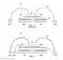
FIG. 1 is a schematic drawing that shows a prior art arrangement for packaging two chips in a single package;
FIG. 2 is a schematic drawing that shows an example arrangement for packaging two chips in a single package, according to teachings of the present disclosure;
FIG. 3 is a schematic drawing showing a step in an example method for packaging two chips in a single package, according to teachings of the present disclosure; and
FIG. 4 is a schematic drawing showing a step in an example method for packaging two chips in a single package, according to teachings of the present disclosure.
DETAILED DESCRIPTION
Teachings of the present disclosure may be embodied in methods for creating a ground shield for stacked die applications. The various embodiments may be employed to reduce noise in multi-chip modules where a “quiet” die is stacked on top of a Fet, or noisy die.
In some embodiments, the noisy die may include one or more extra layers. For example, at the end of fab processing, a layer of oxide may be deposited on the back of the wafer. Post fab, a layer of bondable metal may be deposited on top of the layer of oxide on the back side. The noisy (first) die may be flip-chip mounted to a lead frame, then a second die may be connected on top of the flipped die. The second die may be wire bonding to one or more connections of the lead frame and the bondable metal on the first die may be connected to a voltage source providing a shield potential.
FIG. 1 is a schematic drawing that shows a prior art arrangement for packaging two chips in a single package 10. As shown, a first die 30 may be flip-chip mounted to a lead frame 20. Flip chip mounting may also be referred to as controlled collapse chip connection (C4). In general, flip-chip mounting may be used to interconnect semiconductor devices such as IC chips 30 to external circuitry (e.g., a lead frame). When the IC chip 30 is manufactured, a set of solder bumps 22 are deposited on the top side of the IC chip 30 during the final wafer processing step. To mount IC chip 30 to the lead frame 20, IC chip 30 is ‘flipped’ upside down and aligned with pads 20a, 20b on the lead frame 20. The solder bumps 22 form the bond, e.g., after a solder reflow process.
As shown in FIG. 1, a second die 40 may be mounted on top of the first die 30. The second die 40 may be connected to one or more leads 20c, 20d of the lead frame 20, for example by wire bonding 45.
The first die 30 (or lower die) may include a power transistor and/or additional components that generate a relatively large amount of noise in the voltage (e.g., a field-effect transistor or FET). That voltage noise is, therefore, capacitively coupled to the second die 40 (or upper die).
FIG. 2 is a schematic drawing that shows an example arrangement for packaging two chips in a single package 100, according to teachings of the present disclosure. In the example shown, package 100 may include lower die 120 and upper die 130. As with the package of FIG. 1, the upper die 130 may be stacked on top of the lower die 120.
The lower die 120 may include a so-called “noisy” component and/or die. In some examples, the lower die 120 may include switching power transistors, FETs, MOSFETs, and/or other dies with a noisy voltage signal. Once the various electrical components of lower die 120 have been manufactured (e.g., using various semiconductor manufacturing processes), various additional layers may be deposited on the back side of lower die 120 (discussed in more detail in relation to FIGS. 3 and 4). The lower die 120 is then flip-chip mounted to one or more pads 110c, 110d on a lead frame 110.
The upper die 130 may be stacked on top of the lower die 120. In some embodiments, a non-conductive adhesive 140 (e.g., an epoxy) may be used to connect the upper die 130 to the lower die 120. The various leads of the upper die 130 may be connected to leads 110a, 110e of the lead frame 110 using wire bonding 135. In some embodiments, a layer of metal on the back side of the lower die 120 may be connected to one or more pads 110b on the lead frame 110. This connection may be used to provide a shielding voltage to the metal layer and thereby shield the upper die 130, e.g., to eliminate the effect of voltage noise from the bottom die 120 on the top die 130. The shielding voltage may be connected through one of the pins of the leadframe 110. Thus, an external bias or shielding voltage can be applied through such a pin.
The various embodiments may provide for a low cost stacking arrangement with a greatly increased noise immunity. After the upper die 130 and the lower die 120 are stacked and connected (e.g., to the lead frame 110), the entire arrangement may be encapsulated and/or otherwise treated to provide an integrated circuit package.
FIG. 3 is a schematic drawing showing a step in an example method for packaging two chips in a single package, according to teachings of the present disclosure. As shown in FIG. 3, fabrication processes for the lower die 120a have been completed. At that completion, the lower die 120a includes a substrate or wafer 122. Typically, the circuitry and/or other features of the lower die 120a are processed on the front side of the wafer 122, at the bottom of FIG. 3.
As shown in FIG. 3, an oxide layer 124 is deposited on the back side of wafer 122 or the bottom die 120a. The oxide layer 124 may include various oxides known in the art of semiconductor fabrication.
FIG. 4 is a schematic drawing showing a step in an example method for packaging two chips in a single package, according to teachings of the present disclosure. After the oxide layer 124 is deposited as shown in FIG. 3, a metal layer 126 is deposited on top of the oxide layer 124. The metal layer 126 can then be connected to a shield potential to create the stacked arrangement shown in FIG. 2. The metal layer 126 may be bonded to a fixed voltage source and/or potential to protect the upper die 130 and/or any components thereon from the noisy voltage signal of the lower die 120b.
Claims
1. An integrated circuit package comprising:
a lead frame;
a first die mounted on the lead frame in flip-chip fashion, with a frontside of the first die connected to the lead frame;
wherein the first die comprises an oxide layer deposited on a backside of the first die and a back metal layer deposited on the oxide layer; and
a second die mounted on the back metal layer of the first die;
wherein the oxide layer and the back metal layer both cover a full extent of the backside of the first die and do not extend beyond edges of the first die.
2. The integrated circuit package according to claim 1, wherein the second die is mounted on the back metal layer with an adhesive.
3. The integrated circuit package according to claim 1, wherein the second die is mounted on the back metal layer with a non conductive epoxy.
4. The integrated circuit package according to claim 1, further comprising bumps connecting the first die to the lead frame.
5. The integrated circuit package according to claim 1, further comprising the back metal layer wire bonded to a finger of the lead frame.
6. The integrated circuit package according to claim 1, wherein the first die comprises a power semiconductor.
7. The integrated circuit package according to claim 1, wherein the second die comprises a controller.
8. The integrated circuit package according to claim 1, wherein the second die comprises a circuit sensitive to noise.
9. The integrated circuit package according to claim 1, wherein:
the first die comprises a power semiconductor; and
the second die comprises a controller.
10. A circuit comprising:
a lead frame;
a first die mounted on the lead frame in flip-chip fashion, with the front of the first die connected to the lead frame;
wherein the first die comprises an oxide layer deposited on the back of the first die and a back metal layer deposited on the oxide layer;
a second die mounted on the back metal layer of the first die;
the back metal layer wire bonded to a finger of the lead frame; and
a voltage source providing a shielding voltage fed to the back metal layer through the finger;
wherein the oxide layer and the back metal layer both cover a full extent of the backside of the first die and do not extend beyond edges of the first die.
11. A method for manufacturing a semiconductor device, comprising:
manufacturing a first semiconductor die comprising at least one semiconductor device;
depositing an oxide layer on a back side of the die; and
depositing a back metal layer on top of the oxide layer;
wherein the oxide layer and the back metal layer both cover a full extent of the backside of the first die and do not extend beyond edges of the first die.
12. The method according to claim 11, further comprising:
mounting the first die on a lead frame in flip-chip fashion;
mounting a second die on top of the first die using an adhesive;
wire bonding the back metal layer with one of a plurality of lead frame fingers;
wire bonding the second die with a different one of the plurality of lead frame fingers.
13. The method according to claim 11, further comprising encapsulating the semiconductor device.
14. A method of operating an integrated circuit package including a lead frame, a first die mounted on the lead frame in flip-chip fashion, with the front of the first die connected to the lead frame, wherein the first die comprises an oxide layer deposited on the back of the first die and a back metal layer deposited on the oxide layer, a second die mounted on the back metal layer of the first die, the back metal layer wire bonded to a finger of the lead frame, wherein the oxide layer and the back metal layer both cover a full extent of the backside of the first die and do not extend beyond edges of the first die and a voltage source providing a shielding voltage fed to the back metal layer through the finger, the method comprising:
generating a shielding voltage;
feeding the shielding voltage to said finger of the lead frame; and
operating a circuit and devices within the first and second dies.
15. The method according to claim 14, further comprising a controller in the second die controlling at least one power transistor in the first die.
Images & Drawings included:


Sources:
- United States Patent and Trademark Office - verify current appl. status at the USPTO↗
Recent applications in this class:
- » 20250293178 2025-09-18
SEMICONDUCTOR DEVICE AND METHOD OF MANUFACTURING THEREOF - » 20250293177 2025-09-18
SYSTEMS AND METHODS FOR COMPONENT ISOLATION - » 20250293176 2025-09-18
SYSTEMS AND METHODS FOR COMPONENT ISOLATION - » 20250285991 2025-09-11
SYSTEM IN PACKAGE MODULE AND METHOD FOR FABRICATING THE SAME - » 20250285990 2025-09-11
SHIELDING PARTICLES COATED WITH ELECTRICAL INSULATION - » 20250273595 2025-08-28
Semiconductor Device and Method for Selective EMI Shielding Using a Mask - » 20250273594 2025-08-28
Semiconductor Device and Method of Forming Multi-Layer Shielding Structure Over the Semiconductor Device - » 20250273593 2025-08-28
Component Carrier With Cavity and Laser Protection Structure - » 20250273592 2025-08-28
PARTIALLY SHIELDED SEMICONDUCTOR DEVICE AND METHOD FOR FORMING THE SAME - » 20250273591 2025-08-28
ADDING SACRIFICIAL TRACES TO ABORB SIGNAL INTERFERENCE FROM HIGH SPEED AGGRESSOR TRACES
Recent applications for this Assignee:
- » 20250294824 2025-09-18
TRANSISTOR AND METHOD FOR MANUFACTURING SAME - » 20250294800 2025-09-18
TRANSISTOR AND METHOD FOR MANUFACTURING SAME - » 20250294794 2025-09-18
HIGH ELECTRON MOBILITY TRANSISTOR AND METHOD FOR MANUFACTURING SAME - » 20250291511 2025-09-18
SYSTEM AND METHOD FOR TRAINING SPI MONITOR FOR HIGH-FREQUENCY OPERATION - » 20250291379 2025-09-18
System and Method for Providing High-Frequency Anti-Tamper Protection in Communication Interface - » 20250290224 2025-09-18
HIGH DEFECT SiC WAFER WITH DEVICE LAYER AND METHODS OF MANUFACTURE - » 20250286562 2025-09-11
MICROCONTROLLER INCLUDING A DIGITAL POTENTIOMETER - » 20250285990 2025-09-11
SHIELDING PARTICLES COATED WITH ELECTRICAL INSULATION - » 20250284599 2025-09-11
SYSTEM AND METHOD FOR RECONSTRUCTING DATA FROM A DEGRADED RAID VOLUME USING AN ACCELERATOR ENGINE - » 20250284365 2025-09-11
ELECTRONIC DEVICE INCLUDING A TOUCH DETECTION SYSTEM AND A NOISE DETECTION SYSTEM