Semiconductor device with substrate temperature monitor circuit
US20170317664A1
2017-11-02
15/520,636
2015-01-20
✅ Patent granted
US 10,505,518 B2
2019-12-10
WO; PCT/JP2015/051393; 20150120
WO; WO2016/117030; 20160728
Jared Fureman | Michael J Warmflash
Studebaker & Brackett PC
2035-04-07
Abstract:
First and second circuits, a photocoupler and a substrate temperature monitor circuit are formed on a substrate. A photocoupler includes a primary-side light emitting diode that converts an electric signal received from the first circuit into an optical signal, and a light receiving device that converts the optical signal into an electric signal and outputs the electric signal to the second circuit. The substrate temperature monitor circuit reads a Vf voltage value of the primary-side light emitting diode of the photocoupler to monitor temperature of the substrate.
Inventors:
- Hideo KOMO 11 🇯🇵 Tokyo, Japan
- Takeshi OMARU 8 🇯🇵 Tokyo, Japan
- Koichi TAGUCHI 3 🇯🇵 Fukuoka, Japan
Assignee:
- MITSUBISHI ELECTRIC CORPORATION 16,560 🇯🇵 TOKYO, Japan
Applicant:
Interested in similar patents?
Get notified when new applications in this technology area are published.
Classification:
G01K3/10 » CPC further
Thermometers giving results other than momentary value of temperature giving differences of values ; giving differentiated values in respect of time, e.g. reacting only to a quick change of temperature
G01K7/00 » CPC further
Measuring temperature based on the use of electric or magnetic elements directly sensitive to heat ; Power supply therefor, e.g. using thermoelectric elements
H03K3/017 » CPC further
Circuits for generating electric pulses; Monostable, bistable or multistable circuits; Details Adjustment of width or dutycycle of pulses
H01G9/0003 » CPC further
Electrolytic capacitors, rectifiers, detectors, switching devices, light-sensitive or temperature-sensitive devices; Processes of their manufacture Protection against electric or thermal overload; cooling arrangements; means for avoiding the formation of cathode films
G01K7/01 » CPC further
Measuring temperature based on the use of electric or magnetic elements directly sensitive to heat ; Power supply therefor, e.g. using thermoelectric elements using semiconducting elements having PN junctions
H01L31/12 » CPC further
Semiconductor devices sensitive to infra-red radiation, light, electromagnetic radiation of shorter wavelength or corpuscular radiation and specially adapted either for the conversion of the energy of such radiation into electrical energy or for the control of electrical energy by such radiation; Processes or apparatus specially adapted for the manufacture or treatment thereof or of parts thereof; Details thereof structurally associated with, e.g. formed in or on a common substrate with, one or more electric light sources, e.g. electroluminescent light sources, and electrically or optically coupled thereto
H01G9/00 IPC
Electrolytic capacitors, rectifiers, detectors, switching devices, light-sensitive or temperature-sensitive devices; Processes of their manufacture
H01L25/16 IPC
Assemblies consisting of a plurality of individual semiconductor or other solid state devices ; Multistep manufacturing processes thereof the devices being of types provided for in two or more different main groups of - , e.g. forming hybrid circuits
H01G9/28 » CPC further
Electrolytic capacitors, rectifiers, detectors, switching devices, light-sensitive or temperature-sensitive devices; Processes of their manufacture Structural combinations of electrolytic capacitors, rectifiers, detectors, switching devices with other electric components not covered by this subclass
H01L31/167 » CPC further
Semiconductor devices sensitive to infra-red radiation, light, electromagnetic radiation of shorter wavelength or corpuscular radiation and specially adapted either for the conversion of the energy of such radiation into electrical energy or for the control of electrical energy by such radiation; Processes or apparatus specially adapted for the manufacture or treatment thereof or of parts thereof; Details thereof structurally associated with, e.g. formed in or on a common substrate with, one or more electric light sources, e.g. electroluminescent light sources, and electrically or optically coupled thereto the semiconductor device sensitive to radiation being controlled by the light source or sources the light sources and the devices sensitive to radiation all being semiconductor devices characterised by at least one potential or surface barrier
H01L25/167 » CPC further
Assemblies consisting of a plurality of individual semiconductor or other solid state devices ; Multistep manufacturing processes thereof the devices being of types provided for in two or more different main groups of - , e.g. forming hybrid circuits comprising optoelectronic devices, e.g. LED, photodiodes
H03K3/011 » CPC main
Circuits for generating electric pulses; Monostable, bistable or multistable circuits; Details Modifications of generator to compensate for variations in physical values, e.g. voltage, temperature
Description
FIELD
The present invention relates to a semiconductor device capable of monitoring a substrate temperature without the need for adding any components.
BACKGROUND
A control system for a semiconductor device is required to achieve a high precision, a high functionality, and a high packaging density at a low cost. In the control system, an improvement in the precision of various sensing functions is one of important problems to be solved to achieve an improvement in the efficiency of the semiconductor device. One of impediments to the achievement of an improvement in precision is a variation in performance due to temperature characteristics of electronic components. Accordingly, it is necessary to take some measures to reduce the variation in performance.
Note that a photocoupler is an electronic component that is generally used to transmit signals from a logic part and a semiconductor device, while providing electrical isolation between the logic part and the semiconductor device. A technique in which a light emitting diode of a photocoupler detects abnormal heat generation in the photocoupler has been proposed (e.g., see PTL 1).
CITATION LIST
Patent Literature
- [PTL 1] JP 2007-201169 A
SUMMARY
Technical Problem
To reduce a variation in performance of sensing functions due to temperature characteristics of electronic components, it is necessary to monitor the temperature of a substrate and feed back the monitored temperature. Accordingly, monitoring the substrate temperature using a thermocouple or a thermistor causes a problem that the number of components and costs increase.
The present invention has been made to solve the above-mentioned problem, and an object of the present invention is to obtain a semiconductor device capable of monitoring a substrate temperature without the need for adding any components.
Solution to Problem
A semiconductor device according to the present invention includes: a substrate; first and second circuits formed on the substrate; a photocoupler formed on the substrate and including a light emitting diode that converts an electric signal received from the first circuit into an optical signal, and a light receiving device that converts the optical signal into an electric signal and outputs the electric signal to the second circuit; and a substrate temperature monitor circuit reading a Vf voltage value of the light emitting diode of the photocoupler to monitor temperature of the substrate.
Advantageous Effects of Invention
In the present invention, the substrate temperature monitor circuit reads the Vf voltage value of the light emitting diode of the photocoupler to monitor the temperature of the substrate. Therefore, the photocoupler can monitor the temperature of the substrate, without the need for adding a component such as a thermocouple or a thermistor.
BRIEF DESCRIPTION OF THE DRAWINGS
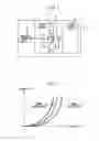
FIG. 1 is a diagram showing a semiconductor device according to Embodiment 1 of the present invention.
FIG. 2 is a graph showing Vf voltage characteristics of the light emitting diode of the photocoupler.
FIG. 3 is a diagram showing a semiconductor device according to Embodiment 2 of the present invention.
FIG. 4 is a diagram showing a semiconductor device according to Embodiment 3 of the present invention.
FIG. 5 is a diagram showing a semiconductor device according to Embodiment 4 of the present invention.
FIG. 6 is a diagram showing a semiconductor device according to Embodiment 5 of the present invention.
FIG. 7 is a diagram showing a semiconductor device according to Embodiment 6 of the present invention.
FIG. 8 is a graph showing a life curve of the aluminum electrolytic capacitor.
FIG. 9 is a diagram showing a semiconductor device according to Embodiment 7 of the present invention.
FIG. 10 is a diagram showing a semiconductor device according to Embodiment 8 of the present invention.
DESCRIPTION OF EMBODIMENTS
A semiconductor device according to the embodiments of the present invention will be described with reference to the drawings. The same components will be denoted by the same symbols, and the repeated description thereof may be omitted.
Embodiment 1
FIG. 1 is a diagram showing a semiconductor device according to Embodiment 1 of the present invention. On a substrate 1, first and second circuits 2 and 3, a photocoupler 4, and a substrate temperature monitor circuit 5 are formed. The photocoupler 4 includes a primary-side light emitting diode 6 that converts an electric signal received from the first circuit 2 into an optical signal, and a light receiving device 7 that converts the optical signal into an electric signal and outputs the electric signal to the second circuit 3. The photocoupler 4 transmits signals from the first circuit 2 and the second circuit 3, while providing electrical isolation between the first circuit 2 and the second circuit 3.
FIG. 2 is a graph showing Vf voltage characteristics of the light emitting diode of the photocoupler. As shown in the figure, the Vf voltage of the primary-side light emitting diode 6 has a temperature dependence. Accordingly, the substrate temperature monitor circuit 5 reads the Vf voltage value of the primary-side light emitting diode 6 of the photocoupler 4, thereby monitoring the temperature of the substrate 1. Since the photocoupler 4 is originally equipped in the device, the photocoupler 4 can monitor the temperature of the substrate 1, without the need for adding a component such as a thermocouple or a thermistor. The monitored temperature is fed back to various sensing circuits to cancel a variation in circuit characteristics due to the temperature, thereby achieving an improvement in the precision of sensing functions.
Embodiment 2
FIG. 3 is a diagram showing a semiconductor device according to Embodiment 2 of the present invention. A constant current circuit 8 is used as a drive circuit for the primary-side light emitting diode 6. With this configuration, substrate temperature information can be accurately monitored.
Embodiment 3
FIG. 4 is a diagram showing a semiconductor device according to Embodiment 3 of the present invention. A power supply circuit 9 supplies a voltage to each of the first and second circuits 2 and 3. The substrate temperature monitor circuit 5 corrects a temperature variation in the output voltage value of the power supply circuit 9 according to the monitored temperature of the substrate 1. Thus, the temperature information is fed back to the power supply circuit 9 and a variation in the power supply voltage value due to temperature characteristics is corrected, thereby making it possible to improve the precision of the drive system for the semiconductor device.
Embodiment 4
FIG. 5 is a diagram showing a semiconductor device according to Embodiment 4 of the present invention. The substrate temperature monitor circuit 5 outputs an error signal when the monitored temperature of the substrate 1 has reached a threshold. A control circuit 10 which has received the error signal interrupts the operation of each of the first and second circuits 2 and 3. Thus, the error signal is output during abnormal heat generation in the substrate 1, thereby making it possible to properly protect the semiconductor device.
Embodiment 5
FIG. 6 is a diagram showing a semiconductor device according to Embodiment 5 of the present invention. A signal output circuit 11 outputs a pulse width modulation (PWM) signal. The substrate temperature monitor circuit 5 corrects a PWM signal according to the monitored temperature of the substrate 1 and supplies the PWM signal to the photocoupler 4. Thus, the temperature is monitored by the substrate temperature monitor circuit 5 and the monitored temperature is fed back, thereby making it possible to correct a variation in transmission of a duty of the PWM signal of the photocoupler 4 that is caused due to temperature characteristics.
Embodiment 6
FIG. 7 is a diagram showing a semiconductor device according to Embodiment 6 of the present invention. The power supply circuit 9 includes an aluminum electrolytic capacitor 12. The substrate temperature monitor circuit 5 refers to a preliminarily stored life curve of the aluminum electrolytic capacitor 12, and accumulates thermal histories of the aluminum electrolytic capacitor 12 from the monitored temperature of the substrate 1, to thereby predict the life of the aluminum electrolytic capacitor 12. FIG. 8 is a graph showing a life curve of the aluminum electrolytic capacitor. Based on this life curve, the life of the aluminum electrolytic capacitor 12 can be accurately predicted.
The substrate temperature monitor circuit 5 outputs an error signal when the predicted life of the aluminum electrolytic capacitor 12 has reached life criteria. An error output part 13 which has received the error signal notifies a user of the error by display, voice, or the like. Thus, the semiconductor device can be properly protected, and a time for replacement of the semiconductor device can be detected.
Embodiment 7
FIG. 9 is a diagram showing a semiconductor device according to Embodiment 7 of the present invention. A plurality of photocouplers 4 is formed on the substrate 1. Although the illustration of the first and second circuits 2 and 3 and the like is omitted, the configurations of these components are similar to those of any one of Embodiments 1 to 6.
The substrate temperature monitor circuit 5 reads the Vf voltage value of the primary-side light emitting diode 6 of each of the plurality of photocouplers 4, and averages the read voltage values, thereby monitoring the temperature of the substrate 1. Thus, the temperature of the substrate is monitored by the plurality of photocouplers 4, thereby making it possible to more accurately monitor the temperature of the substrate 1.
Embodiment 8
FIG. 10 is a diagram showing a semiconductor device according to Embodiment 8 of the present invention. A plurality of photocouplers 4 is formed on the substrate 1. Although the illustration of the first and second circuits 2 and 3 and the like is omitted, the configurations of these components are similar to those of any one of Embodiments 1 to 6.
The substrate temperature monitor circuit 5 reads the Vf voltage value of the primary-side light emitting diode 6 of the photocoupler 4 that is located at a position where the temperature of the substrate 1 is highest among the plurality of photocouplers 4, thereby monitoring the temperature of the substrate 1. Thus, one of the photocouplers 4 is monitored, thereby minimizing the cost and sensing processing.
REFERENCE SIGNS LIST
- 1 substrate; 2 first circuit; 3 second circuit; 4 photocoupler; 5 substrate temperature monitor circuit; 6 primary-side light emitting diode; 7 light receiving device; 8 constant current circuit; 9 power supply circuit; 10 control circuit; 11 signal output circuit; 12 aluminum electrolytic capacitor
Claims
1. A semiconductor device comprising:
a substrate;
first and second circuits formed on the substrate;
a photocoupler formed on the substrate and including a light emitting diode that converts an electric signal received from the first circuit into an optical signal, and a light receiving device that converts the optical signal into an electric signal and outputs the electric signal to the second circuit; and
a substrate temperature monitor circuit reading a Vf voltage value of the light emitting diode of the photocoupler to monitor temperature of the substrate.
2. The semiconductor device according to claim 1, further comprising a constant current circuit that is a drive circuit for the light emitting diode.
3. The semiconductor device according to claim 1, further comprising a power supply circuit supplying a voltage to each of the first and second circuits,
wherein the substrate temperature monitor circuit corrects a temperature variation in an output voltage value of the power supply circuit according to the monitored temperature of the substrate.
4. The semiconductor device according to claim 1, wherein the substrate temperature monitor circuit outputs an error signal when the monitored temperature of the substrate has reached a threshold.
5. The semiconductor device according to claim 1, further comprising a signal output circuit outputing a pulse width modulation signal,
wherein the substrate temperature monitor circuit corrects the pulse width modulation signal according to the monitored temperature of the substrate and supplying the corrected pulse width modulation signal to the photocoupler.
6. The semiconductor device according to claim 1, further comprising a power supply circuit supplying a voltage to each of the first and second circuits,
wherein the power supply circuit includes an aluminum electrolytic capacitor, and
the substrate temperature monitor circuit accumulates thermal histories of the aluminum electrolytic capacitor from the monitored temperature of the substrate to predict a life of the aluminum electrolytic capacitor.
7. The semiconductor device according to claim 6, wherein the substrate temperature monitor circuit outputs an error signal when the predicted life of the aluminum electrolytic capacitor has reached life criteria.
8. The semiconductor device according to claim 1, wherein the photocoupler includes a plurality of photocouplers, and
the substrate temperature monitor circuit reads the Vf voltage value of the light emitting diode of each of the plurality of photocouplers and averages the read voltage values to monitor the temperature of the substrate.
9. The semiconductor device according to claim 1, wherein the photocoupler includes a plurality of photocouplers, and
the substrate temperature monitor circuit reads the Vf voltage value of the light emitting diode of the photocoupler that is located at a position where the temperature of the substrate is highest among the plurality of photocouplers to monitor the temperature of the substrate.
Images & Drawings included:


Sources:
- United States Patent and Trademark Office - verify current appl. status at the USPTO↗
Recent applications in this class:
- » 20250286536 2025-09-11
VARIATION COMPENSATION OF POWER SEMICONDUCTORS - » 20250088177 2025-03-13
ULTRA-LOW POWER TIMING CIRCUIT WITH PLL LOCKING - » 20250088176 2025-03-13
SIGNAL DRIVER CIRCUIT, AND A SEMICONDUCTOR APPARATUS USING THE SAME - » 20250080087 2025-03-06
PARASITIC CAPACITANCE MITIGATION CIRCUIT FOR RELAXATION OSCILLATORS - » 20250047265 2025-02-06
DRIVE SIGNAL SUPPLY DEVICE AND DRIVE SIGNAL CALIBRATING METHOD THEREOF - » 20250038737 2025-01-30
SEMICONDUCTOR DEVICE - » 20240429899 2024-12-26
CONDITIONAL ACTIVE THERMAL CONTROL TO INCREASE POWER SEMICONDUCTOR LIFETIME AND EFFICIENCY - » 20240421802 2024-12-19
FREQUENCY GENERATOR AND FREQUENCY CORRECTION METHOD FOR FREQUENCY GENERATOR - » 20240405756 2024-12-05
Desaturation circuit having temperature compensation - » 20240388277 2024-11-21
ELECTRONIC CIRCUIT
Recent applications for this Assignee:
- » 20250294680 2025-09-18
POWER MODULE - » 20250293740 2025-09-18
WIRELESS COMMUNICATION SYSTEM - » 20250293196 2025-09-18
SEMICONDUCTOR DEVICE AND MANUFACTURING METHOD THEREOF - » 20250291113 2025-09-18
OPTICAL TERMINATOR, OPTICAL WAVELENGTH FILTER, AND EXTERNAL CAVITY LASER LIGHT SOURCE - » 20250290867 2025-09-18
SEMICONDUCTOR INSPECTION APPARATUS AND METHOD OF MANUFACTURING SEMICONDUCTOR DEVICE - » 20250290765 2025-09-18
INFORMATION PROCESSING DEVICE, INFORMATION PROCESSING METHOD, AND IMAGE PROJECTING SYSTEM - » 20250289592 2025-09-18
SPACE SITUATIONAL AWARENESS BUSINESS DEVICE AND SPACE TRAFFIC BUSINESS DEVICE - » 20250287683 2025-09-11
SEMICONDUCTOR DEVICE - » 20250287624 2025-09-11
POWER SEMICONDUCTOR DEVICE - » 20250287098 2025-09-11
DETECTION DEVICE, CAMERA SYSTEM, DETECTION METHOD, AND STORAGE MEDIUM STORING DETECTION PROGRAM