Electron transport material, an OLED display panel and an electronic device compromising the same
US20170338422A1
2017-11-23
15/673,327
2017-08-09
✅ Patent granted
US 11,133,476 B2
2021-09-28
-
-
Dylan C Kershner
Alston & Bird LLP
2039-04-23
Abstract:
The present disclosure relates to an electron transport material having a structure represented by formula (I). The present disclosure enhances the glass transition temperature of the material by way of increasing the molecular weight thereof through modifying phenanthroline, without influencing the electron transport property of the material. A novel type of electron transport material having a glass transition temperature of more than 100° C. is designed by the present disclosure. The compound provided by the present disclosure is used as an electron transport material, i.e. as an electron transport layer; and the compound is doped with metals for use as an electron injection layer, thereby improving the efficiency of an OLED device and reducing the operation voltage.
Inventors:
- Ying Liu 38 🇨🇳 Shanghai, China
- Xiangcheng WANG 72 🇨🇳 Shanghai, China
- Yuji HAMADA 39 🇨🇳 Shanghai, China
- Jinghua NIU 104 🇨🇳 Shanghai, China
- Miao WANG 14 🇨🇳 Shanghai, China
Assignee:
- Shanghai Tianma AM-OLED Co., Ltd 374 🇨🇳 Shanghai, China
Applicant:
Interested in similar patents?
Get notified when new applications in this technology area are published.
Classification:
H01L51/0072 » CPC main
Solid state devices using organic materials as the active part, or using a combination of organic materials with other materials as the active part; Processes or apparatus specially adapted for the manufacture or treatment of such devices, or of parts thereof; Selection of organic semiconducting materials, e.g. organic light sensitive or organic light emitting materials; Macromolecular systems with low molecular weight, e.g. cyanine dyes, coumarine dyes, tetrathiafulvalene aromatic compounds comprising a hetero atom, e.g.: N,P,S; Polycyclic condensed heteroaromatic hydrocarbons comprising only nitrogen in the heteroaromatic polycondensed ringsystem, e.g. phenanthroline, carbazole
H01L51/50 IPC
Solid state devices using organic materials as the active part, or using a combination of organic materials with other materials as the active part; Processes or apparatus specially adapted for the manufacture or treatment of such devices, or of parts thereof specially adapted for light emission, e.g. organic light emitting diodes [OLED] or polymer light emitting devices [PLED]
H01L51/0058 » CPC further
Solid state devices using organic materials as the active part, or using a combination of organic materials with other materials as the active part; Processes or apparatus specially adapted for the manufacture or treatment of such devices, or of parts thereof; Selection of organic semiconducting materials, e.g. organic light sensitive or organic light emitting materials; Macromolecular systems with low molecular weight, e.g. cyanine dyes, coumarine dyes, tetrathiafulvalene; Polycyclic condensed aromatic hydrocarbons, e.g. anthracene containing more than one polycyclic condensed aromatic rings, e.g. bis-anthracene
H01L51/52 IPC
Solid state devices using organic materials as the active part, or using a combination of organic materials with other materials as the active part; Processes or apparatus specially adapted for the manufacture or treatment of such devices, or of parts thereof specially adapted for light emission, e.g. organic light emitting diodes [OLED] or polymer light emitting devices [PLED] Details of devices
H01L51/0067 » CPC further
Solid state devices using organic materials as the active part, or using a combination of organic materials with other materials as the active part; Processes or apparatus specially adapted for the manufacture or treatment of such devices, or of parts thereof; Selection of organic semiconducting materials, e.g. organic light sensitive or organic light emitting materials; Macromolecular systems with low molecular weight, e.g. cyanine dyes, coumarine dyes, tetrathiafulvalene aromatic compounds comprising a hetero atom, e.g.: N,P,S comprising only nitrogen as heteroatom
H01L51/5012 » CPC further
Solid state devices using organic materials as the active part, or using a combination of organic materials with other materials as the active part; Processes or apparatus specially adapted for the manufacture or treatment of such devices, or of parts thereof specially adapted for light emission, e.g. organic light emitting diodes [OLED] or polymer light emitting devices [PLED] Electroluminescent [EL] layer
H01L51/5056 » CPC further
Solid state devices using organic materials as the active part, or using a combination of organic materials with other materials as the active part; Processes or apparatus specially adapted for the manufacture or treatment of such devices, or of parts thereof specially adapted for light emission, e.g. organic light emitting diodes [OLED] or polymer light emitting devices [PLED]; Carrier transporting layer Hole transporting layer
H01L51/5072 » CPC further
Solid state devices using organic materials as the active part, or using a combination of organic materials with other materials as the active part; Processes or apparatus specially adapted for the manufacture or treatment of such devices, or of parts thereof specially adapted for light emission, e.g. organic light emitting diodes [OLED] or polymer light emitting devices [PLED]; Carrier transporting layer Electron transporting layer
H01L51/5088 » CPC further
Solid state devices using organic materials as the active part, or using a combination of organic materials with other materials as the active part; Processes or apparatus specially adapted for the manufacture or treatment of such devices, or of parts thereof specially adapted for light emission, e.g. organic light emitting diodes [OLED] or polymer light emitting devices [PLED] Carrier injection layer
H01L51/5092 » CPC further
Solid state devices using organic materials as the active part, or using a combination of organic materials with other materials as the active part; Processes or apparatus specially adapted for the manufacture or treatment of such devices, or of parts thereof specially adapted for light emission, e.g. organic light emitting diodes [OLED] or polymer light emitting devices [PLED]; Carrier injection layer Electron injection layer
H01L51/5206 » CPC further
Solid state devices using organic materials as the active part, or using a combination of organic materials with other materials as the active part; Processes or apparatus specially adapted for the manufacture or treatment of such devices, or of parts thereof specially adapted for light emission, e.g. organic light emitting diodes [OLED] or polymer light emitting devices [PLED]; Details of devices; Electrodes Anodes, i.e. with high work-function material
H01L51/5221 » CPC further
Solid state devices using organic materials as the active part, or using a combination of organic materials with other materials as the active part; Processes or apparatus specially adapted for the manufacture or treatment of such devices, or of parts thereof specially adapted for light emission, e.g. organic light emitting diodes [OLED] or polymer light emitting devices [PLED]; Details of devices; Electrodes Cathodes, i.e. with low work-function material
H01L2251/301 » CPC further
Indexing scheme relating to organic semiconductor devices covered by group; Materials Inorganic materials
H01L2251/308 » CPC further
Indexing scheme relating to organic semiconductor devices covered by group; Materials; Inorganic materials; Oxides, e.g. metal oxides; Transparent conductive oxides [TCO] composed of indium oxides, e.g. ITO
H01L51/00 IPC
Solid state devices using organic materials as the active part, or using a combination of organic materials with other materials as the active part; Processes or apparatus specially adapted for the manufacture or treatment of such devices, or of parts thereof
C07D519/00 » CPC further
Heterocyclic compounds containing more than one system of two or more relevant hetero rings condensed among themselves or condensed with a common carbocyclic ring system not provided for in groups or
H01L51/0052 » CPC further
Solid state devices using organic materials as the active part, or using a combination of organic materials with other materials as the active part; Processes or apparatus specially adapted for the manufacture or treatment of such devices, or of parts thereof; Selection of organic semiconducting materials, e.g. organic light sensitive or organic light emitting materials; Macromolecular systems with low molecular weight, e.g. cyanine dyes, coumarine dyes, tetrathiafulvalene Polycyclic condensed aromatic hydrocarbons, e.g. anthracene
C07D471/04 » CPC further
Heterocyclic compounds containing nitrogen atoms as the only ring hetero atoms in the condensed system, at least one ring being a six-membered ring with one nitrogen atom, not provided for by groups - in which the condensed system contains two hetero rings Ortho-condensed systems
Description
CROSS-REFERENCE TO RELATED APPLICATIONS
This application claims priority of Chinese Patent Application No. CN201710081427.2, filed on Feb. 15, 2017, the entire contents of which are hereby incorporated by reference.
TECHNICAL FIELD
The present disclosure relates to the field of organic electroluminescent materials, and especially to an electron transport material, an OLED display panel and an electronic device comprising the same, and more particularly to the synthesis of a nitrogen-containing electron transport material and its application in an organic electroluminescent device.
BACKGROUND
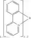
Bphen (4,7-diphenyl-1,10-phenanthroline)
with low molecular weight has a relatively high electron mobility (5.2×10⁻⁴ cm2/Vs, 5.5×10⁵ V/cm) due to its rigid plane structure, and is therefore widely used as the material for an electron transport layer for an organic light emission display device.
CN101121715B discloses a phenanthroline derivative compound and a method for producing it, and its application as an electron transport material, in a light emitting element of a light emitting device. A phenanthroline derivative compound is represented by its molecular formular
wherein Arl represents an aryl group, preferably a substituted or unsubstituted phenyl group, a substituted or unsubstituted naphthyl group, a substituted or unsubstituted anthryl group, or a substituted or unsubstituted phenanthryl group. As the preferred compounds, for example, TMPBP, NaBP, and PBPE, and the like can be listed. In the light emitting element, the light emitting device, and the electronic device, it is preferable that the compound is contained in the light emitting layer. In this case, it is preferable to use the compound as the main body.
However, the existing phenanthroline compound has a relatively too low glass transition temperature Tg of only 62° C., although it can form a non-crystalline film in the vacuum evaporation, the device is susceptible to decay when in operation, thereby affecting the stability of the device.
Therefore, a technical problem to be solved in the art is how to develop a phenanthroline-based electron transport material with a higher glass transition temperature, and how to use the electron transport material to produce an electron transport layer and an electron injection layer.
SUMMARY
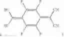
In view of the deficiencies in the related technics, the first objective of the present disclosure is to provide an electron transport material having a structure represented by formula (I):
in formula (I), a, b and c are each independently selected from the group consisting of CR4 and N; wherein R4 is any one or a combination of at least two selected from the group consisting of a hydrogen atom, a substituted or unsubstituted hydrocarbyl, a heterocyclic group, a halogen atom, a nitro group, a cyano group,
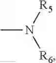
—OR7, —SR8 and —COOR9; wherein, R5, R6, R7, R8, and R9 are each independently any one or a combination of at least two selected from the group consisting of a hydrogen atom, a substituted or unsubstituted hydrocarbyl, and a heterocyclic group;
in formula (I), R1, R2, and R3 are each independently any one or a combination of at least two selected from the group consisting of a hydrogen atom, a deuterium atom, a substituted or unsubstituted hydrocarbyl, and a heterocyclic group.
The second objective of the present disclosure is to provide an OLED display panel comprising a first electrode and a second electrode, wherein a laminate comprising a light emitting layer and an electron transport layer is disposed between the first electrode and the second electrode, and the material of the electron transport layer includes an electron transport material as described in the first object of the present disclosure.
The third objective of the present disclosure is to provide an electronic device comprising an OLED display panel as described in the second object of the present disclosure.
DESCRIPTION OF THE DRAWINGS
FIG. 1 is a cross-sectional structural representation of an OLED display panel provided in a specific embodiment of the present disclosure.
FIG. 2 is a cross-sectional structural representation of another OLED display panel provided in a specific embodiment of the present disclosure.
FIG. 3 is a cross-sectional structural representation of still another OLED display panel provided in a specific embodiment of the present disclosure.
FIG. 4 is a cross-sectional structural representation of still another OLED display panel provided in a specific embodiment of the present disclosure.
DETAILED DESCRIPTION
For the purpose of understanding the present disclosure, the following examples are listed below in the present disclosure. It will be apparent to those skilled in the art that the examples are merely illustrations of the present disclosure and should not be construed as specific limitations of the present disclosure.
In one specific embodiment, the present disclosure provides an electron transport material having a structure represented by formula (I):
in formula (I), a, b and c are each independently selected from the group consisting of CR4 and N; wherein R4 is any one or a combination of at least two selected from the group consisting of a hydrogen atom, a substituted or unsubstituted hydrocarbyl, a heterocyclic group, a halogen atom, a nitro group, a cyano group,
—OR7, —SR8 and —COOR9; wherein, R5, R6, R7, R8, and R9 are each independently any one or a combination of at least two selected from the group consisting of a hydrogen atom, a substituted or unsubstituted hydrocarbyl, and a heterocyclic group;
in formula (I), R1, R2, and R3 each independently represents any one or a combination of at least two selected from the group consisting of a hydrogen atom, a deuterium atom, a substituted or unsubstituted hydrocarbyl, and a heterocyclic group. The present disclosure enhances the glass transition temperature of a material by way of increasing the molecular weight thereof through modifying the phenanthroline, meanwhile without influencing the electron transport property of the material, whereby a novel type of electron transport material having a glass transition temperature of more than 100° C. is designed by the present disclosure.
Preferably, the substituted or unsubstituted hydrocarbyl includes any one or a combination of at least two of a substituted or unsubstituted C1-C30 linear or branched alkyl group, a substituted or unsubstituted C3-C20 cycloalkyl group, a substituted or unsubstituted C2-C20 alkenyl group, a substituted or unsubstituted C2-C20 alkynyl group, and an aromatic group.
Preferably, in formula (I), R1, R2, and R3 each independently represents any one or a combination of at least two selected from the group consisting of
In a preferred specific embodiment, in formula (I), a, b and c are each independently selected from the group consisting of CR4 and N; wherein R4 is any one selected from the group consisting of a hydrogen atom, a deuterium atom, a halogen, a nitro group, a cyano group, a trifluoromethyl group, a C1-C8 linear alkyl group or branched alkyl group, a C6-C34 aryl group or a C2-C34 nitrogen-containing heterocyclic aryl.
In formula (I), R1, R2, and R3 are each independently any one selected from the group consisting of a hydrogen atom, a deuterium atom, a halogen, a nitro group, a cyano group, a trifluoromethyl group, and the structure of (R5)d—R6—,
In the structure of (R5)d—R6—, R6 is a C6-C34 aryl or a C2-C34 nitrogen containing heterocyclic aryl, R5 is any one of a hydrogen atom, a deuterium atom, a halogen, a nitro group, a cyano group or a trifluoromethyl group, and d is an integer more than 1.
In the structure of
R7 is any one of a C1-C4 alkyl, a C6-C12 aryl and a C6-C12 nitrogen containing heterocyclic aryl; or,
-
- in the structure of
R8 is a C1-C4 alkyl, a C6-C12 aryl and a C6-C12 nitrogen containing heterocyclic aryl; or,
-
- in the structure of
R9 and R10 are each independently selected from a C6-C12 aryl and a C6-C12 nitrogen containing heterocyclic aryl.
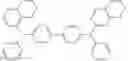
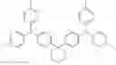
In a preferred specific embodiment, in formula (I), R1, R2, and R3 are each independently any one or a combination of at least two selected from the group consisting of H—, D-, CN—, CF3—, NO2—, F—, Cl, Br—,
and the like; and further preferably selected from the group consisting of
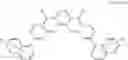
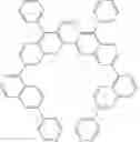
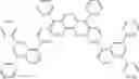
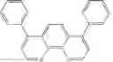
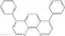
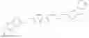
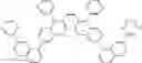
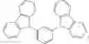
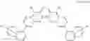
In a preferred specific embodiment, the electron transport material of the present disclosure comprises any one or a combination of at least two of
Illustratively, the electron transport material of the present disclosure comprises:
and the like.
The compounds having the structure represented by formula (I) provided by the present disclosure can be synthesized through the related technics, and the specific synthetic route includes the following steps:
Step (1):
Step (2):
Exemplary preparation method, such as for
includes the following steps:
Step 1: Synthesis of intermediate a
100 mL of n-butyl methyl ether is charged into a three-necked flask, and 1 mol of 1,2-diiodobenzene (raw material 1) and 2.2 mol of intermediate 2 are added thereto respectively under stirring to react therewith for 3 days at 80° C., and the solvent is removed by distillation under reduced pressure to give intermediate 3. Then, 30 mL of acetic acid is added to the three-necked flask, followed by the addition of 3 drops of concentrated sulfuric acid (98%) to react at 100° C. for 20 minutes. After the completion of reaction, the mixture is diluted with water and extracted with dichloromethane, the organic phase is washed with water and then dried over anhydrous sodium sulfate, the dichloromethane is removed by distillation to obtain the intermediate a (yield: 50%).
Step 2:
The intermediate a (1 mol) and intermediate 4 (2.2 mol) are dissolved in 100 mL of a solution of toluene in ethanol (a ratio of 5:1 by volume), followed by the addition of tetrakis(triphenylphosphine)palladium (1 mmol), and a solvent of 1% KOH (20 mL), then the reaction system is vacuumized and filled with nitrogen, and heated to reflux for 20 hours. After cooling, the solvent is removed by distillation under reduced pressure and the obtained product is extracted with dichloromethane. The organic phase is washed with water and then dried over anhydrous sodium sulfate, the dichloromethane is distilled off The crude product is eluted with a mobile phase of CH2Cl2 and ethyl acetate in a gradient elution to obtain the target product b (yield: about 83%).
Exemplary preparation method, such as for molecule
includes the following steps:
Step 1:
Step 2:
The yield of the above synthesis is about 80%.
Exemplary preparation method, such as for
includes the following steps:
Step 1:
Step 2:
The yield of the above synthesis is about 70%.
In a specific embodiment, the present disclosure also provides an OLED display panel comprising a first electrode and a second electrode, wherein a laminate comprising a light emitting layer and an electron transport layer is disposed between the first electrode and the second electrode, and the material of the electron transport layer includes the electron transport material as previously described.
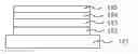
The OLED display panel exemplarily has a structure as shown in FIG. 1, which comprises a substrate 101, a first electrode 102 disposed on the substrate 101, a light emitting layer 103 and an electron transport layer 104 sequentially laminated on the first electrode 102, and a second electrode 105 formed thereon.
The electron transport layer 104 has a compound with a structure represented by formula (I).
In a specific embodiment, the laminate further comprises an electron injection layer, the material of the electron injection layer includes the electron transport material as previously described and a doped metal.
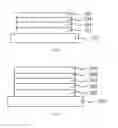
The OLED display panel exemplarily has a structure as shown in FIG. 2, which comprises a substrate 201, a first electrode 202 disposed on the substrate 201, a light emitting layer 203, an electron transport layer 204 and an electron injection layer 206 sequentially laminated on the first electrode 202, and a second electrode 205 formed thereon.
The electron transport layer 204 has a compound having a structure represented by formula (I), and the electron injection layer 206 includes a compound with a structure represented by formula (I) and a doped metal.
Preferably, the doped metal includes any one or a combination of at least two of sodium, potassium, calcium, cesium and ytterbium, such as a combination of sodium and potassium, a combination of calcium and sodium, a combination of potassium, calcium and ytterbium, a combination of calcium, cesium and ytterbium, and a combination of sodium, potassium and cesium, and the like.
Preferably, in the electron injection material, the content of the doped metal is 1-5 wt %, for example 1.2 wt %, 1.5 wt %, 1.7 wt %, 1.9 wt %, 2.1 wt %, 2.3 wt %, 2.5 wt %, 2.7 wt %, 3.0 wt %, 3.3 wt %, 3.5 wt %, 3.7 wt %, 3.9 wt %, 4.2 wt %, 4.6 wt %, and 4.8 wt %, and the like.
In a specific embodiment, the laminate further comprises any one or a combination of at least two of a hole injection layer and a hole transport layer.
In a specific embodiment, the OLED display panel comprises from bottom to top a first electrode, a hole injection layer, a hole transport layer, a light emitting layer, an electron transport layer, an electron injection layer, and a second electrode in sequence.
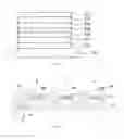
The OLED display panel exemplarily has a structure as shown in FIG. 3, which comprises a substrate 301, a first electrode 302 disposed on the substrate 301, a hole injection layer 307, a hole transport layer 308, a light emitting layer 303, an electron transport layer 304 and an electron injection layer 306 sequentially laminated on the first electrode 302, and a second electrode 305 formed thereon.
The electron transport layer 304 has a compound with a structure represented by formula (I), and the electron injection layer 306 includes a compound with a structure represented by formula (I) and a doped metal.
The material of the hole injection layer exemplarily includes molybdenum oxide, vanadium oxide, ruthenium oxide, tungsten oxide and manganese oxide, and the like, and may further include phthalocyanine-based compounds such as phthalocyanine, copper phthalocyanine, and the like, and may also include a polymer material such as poly(ethylene dioxythiophene)/poly(styrene sulfonic acid) and the like.
The material of the hole transport layer may exemplarily be an aromatic amine-based materials such as aromatic amine compounds of 4,4′-bis[N-(3-methylphenyl)-N-aniline]biphenyl, NPB (4,4′-bis[N-(1-naphthyl)-N-aniline]biphenyl), and the like.
Preferably, the first electrode is an anode and the second electrode is a cathode.
In a specific embodiment, the first electrode at least comprises a reflective film and a conductive transparent thin film.
In a specific embodiment, the reflective film includes silver.
The conductive transparent thin film is selected from an ITO (indium tin oxide) film and/or an IZO (indium zinc oxide) film.
In a specific embodiment, the second electrode is selected from any one of magnesium silver alloy, silver metal, silver ytterbium alloy and silver rare-earth metal alloy.
In a further specific embodiment, the OLED display panel of the present disclosure exemplarily has a structure as shown in FIG. 4, which comprises a lower substrate 10 and an upper substrate (or a package film layer) 20, an array of TFT (thin film transistor) 11, an anode 12, a light emitting layer 13R corresponding to the R pixel region, a light emitting layer 13G corresponding to the G pixel region, a light emitting layer 13B corresponding to the B pixel region, and a cathode 15 on the lower substrate 10. In a specific embodiment, the present disclosure also provides an electronic device comprising the OLED display panel as previously described.
EXAMPLES
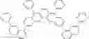
Example 1
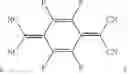
An OLED display panel, the structure of the device is as follows: a substrate 301, a first electrode 302 (ITO electrode), a hole injection layer F4-TCNQ
NPB
(1%, 10 nm), a hole transport layer TAPC
(125 nm), a light emitting layer DPVBi
BCzVBi
(5%, 25 nm), an electron transport layer 10 nm, an electron injection layer 34 nm, and a cathode Ag (15 nm) sequentially laminated on the substrate 301.
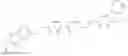
The electron transport layer 304 is
and the electron injection layer 306 includes
doped with 1% of Yb.
Example 2
An OLED display panel, the structure of the device is as follows: a substrate 301, a first electrode 302 (ITO electrode), a hole injection layer F4-TCNQ
NPB
(1%, 10 nm), a hole transport layer TAPC
(125 nm), a light emitting layer DPVBi
BCzVBi
(5%, 25 nm), an electron transport layer 10 nm, an electron injection layer 34 nm, and a cathode Ag (15 nm) sequentially laminated on the substrate 301.
The electron transport layer 304 is
and the electron injection layer 306 includes
doped with 1% of Yb.
Comparative Example 1
An OLED display panel, the structure of the device is as follows: a substrate 301, a first electrode 302 (ITO electrode), a hole injection layer F4-TCNQ
NPB
(1%, 10 nm), a hole transport layer
TAPC
(125 nm), a light emitting layer DPVBi
BCzVBi
(5%, 25 nm), an electron transport layer 10 nm, an electron injection layer 34 nm, and a cathode Ag (15 nm) sequentially laminated on the substrate 301.
The electron transport layer 304 is
and the electron injection layer 306 includes
doped with 1% of Yb.
Example 3
An OLED display panel, the structure of the device is as follows: a substrate 301, a first electrode 302 (ITO electrode), a hole injection layer F4-TCNQ
NPB
(1%, 10 nm), a hole transport layer TAPC
(125 nm), a light emitting layer DPVBi
BCzVBi
(5%, 25 nm), an electron transport layer 10 nm, an electron injection layer 34 nm, and a cathode Ag (15 nm) sequentially laminated on the substrate 301.
The electron transport layer 304 is
and the electron injection layer 306 includes
doped with 1% of Yb.
Example 4
An OLED display panel, the structure of the device is as follows: a substrate 301, a first electrode 302 (ITO electrode), a hole injection layer F4-TCNQ
NPB
(1%, 10 nm), a hole transport layer TAPC
(125 nm), a light emitting layer DPVBi
BCzVBi
(5%, 25 nm), an electron transport layer 10 nm, an electron injection layer 34 nm, and a cathode Ag (15 nm) sequentially laminated on the substrate 301.
The electron transport layer 304 is
and the electron injection layer 306 includes
doped with 1% of Yb.
Example 5
An OLED display panel, the structure of the device is as follows: a substrate 301, a first electrode 302 (ITO electrode), a hole injection layer F4-TCNQ
NPB
(1%, 10 nm), a hole transport layer TAPC
(125 nm), a light emitting layer Ir(ppy)3
mCP
(6%, 35 nm), an electron transport layer 10 nm, an electron injection layer 34 nm, and a cathode Ag (15 nm) sequentially laminated on the substrate 301.
The electron transport layer 304 is
and the electron injection layer 306 includes molecule
doped with 1% of Yb.
Performance Test
The OLED display panels provided in the Examples and the Comparative
Example were subjected to the following performance tests:
Tg was measured using the differential scanning calorimetry, and the external quantum efficiency and voltage of the device were detected using a voltmeter such as the Spectroscan PR 705 spectrometer or Keithley 236 current & voltage source measurement system, and the voltage and external quantum efficiency were determined under a current density of 10 mA/cm2.
The test results were as shown in Table 1.
| TABLE 1 | ||||
| Efficiency, | ||||
| Examples | Voltage, V | Tg, ° C. | EQE | |
| Example 1 | 3.3 | 110 | 6.2% | |
| Comparative | 4 | 62 | 5% | |
| Example 1 | ||||
| Example 2 | 3.2 | 110 | 7.3% | |
| Example 3 | 3.2 | 112 | 7% | |
| Example 4 | 3.4 | 150 | 6.5% | |
| Example 5 | 3.7 | 110 | 30% | |
Applicant has stated that although the detailed process equipment and process flow of the present disclosure have been described by the above examples in the present disclosure, the present disclosure is not limited thereto, that is to say, it is not meant that the present disclosure has to be implemented depending on the above detailed process equipment and process flow. It will be apparent to those skilled in the art that any improvements made to the present disclosure, equivalent replacements to the raw materials of the products of the present disclosure and addition of adjuvant ingredients, and choices of the specific implementations, etc., all fall within the protection scope and the disclosure scope of the present disclosure.
Claims
What is claimed is:1. An electron transport material, comprising a molecular structure represented by formula (I):
wherein in formula (I), a, b and c each is independently selected from the group consisting of CR4 and N; wherein R4 is any one or a combination of at least two selected from the group consisting of a hydrogen atom, a substituted or unsubstituted hydrocarbyl, a heterocyclic group, a halogen atom, a nitro group, a cyano group,
—OR7, —SR8 and —COOR9; wherein, R5, R6, R7, R8, and R9 each is independently formed of any one or a combination of at least two selected from the group consisting of a hydrogen atom, a substituted or unsubstituted hydrocarbyl, and a heterocyclic group; and
wherein in formula (I), R1, R2, and R3 each is independently formed of any one or a combination of at least two selected from the group consisting of a hydrogen atom, a deuterium atom, a substituted or unsubstituted hydrocarbyl, and a heterocyclic group.
2. The electron transport material of claim 1, wherein the substituted or unsubstituted hydrocarbyl comprises any one or a combination of at least two of a substituted or unsubstituted C1-C30 linear or branched alkyl group, a substituted or unsubstituted C3-C20 cycloalkyl group, a substituted or unsubstituted C2-C20 alkenyl group, a substituted or unsubstituted C2-C20 alkynyl group, and an aromatic group.
3. The electron transport material of claim 1, wherein in formula (I), R1, R2, and R3 each is independently formed of any one or a combination of at least two selected from the group consisting of
4. The electron transport material of claim 1, wherein the electron transport material comprises any one or a combination of at least two of
5. An OLED display panel comprising a first electrode and a second electrode, wherein a laminate comprising a light emitting layer and an electron transport layer is disposed between the first electrode and the second electrode, and wherein a material of the electron transport layer has a structure represented by formula (I):
wherein in formula (I), a, b and c each is independently selected from the group consisting of CR4 and N; wherein R4 is any one or a combination of at least two selected from the group consisting of a hydrogen atom, a substituted or unsubstituted hydrocarbyl, a heterocyclic group, a halogen atom, a nitro group, a cyano group,
—OR7, —SR8 and —COOR9; wherein, R5, R6, R7, R8, and R9 each is independently formed of any one or a combination of at least two selected from the group consisting of a hydrogen atom, a substituted or unsubstituted hydrocarbyl, and a heterocyclic group; and
wherein in formula (I), R1, R2, and R3 each is independently formed of any one or a combination of at least two selected from the group consisting of a hydrogen atom, a deuterium atom, a substituted or unsubstituted hydrocarbyl, and a heterocyclic group.
6. The OLED display panel of claim 5, wherein the laminate further comprises an electron injection layer, wherein a material of the electron injection layer includes an electron transport material and a doped metal, wherein the electron transport material has a structure represented by formula (I):
wherein in formula (I), a, b and c are each independently selected from the group consisting of CR4 and N; wherein R4 is any one or a combination of at least two selected from the group consisting of a hydrogen atom, a substituted or unsubstituted hydrocarbyl, a heterocyclic group, a halogen atom, a nitro group, a cyano group,
—OR7, —SR8 and —COOR9; wherein, R5, R6, R7, R8, and R9 each is independently formed of any one or a combination of at least two selected from the group consisting of a hydrogen atom, a substituted or unsubstituted hydrocarbyl, and a heterocyclic group; and
wherein in formula (I), R1, R2, and R3 are each independently any one or a combination of at least two selected from the group consisting of a hydrogen atom, a deuterium atom, a substituted or unsubstituted hydrocarbyl, and a heterocyclic group.
7. The OLED display panel of claim 6, wherein the doped metal includes any one or a combination of at least two of sodium, potassium, calcium, cesium and ytterbium.
8. The OLED display panel of claim 6, wherein the concentration of the doped metal is 1-5 wt % in the electron injection material.
9. The OLED display panel of claim 5, wherein the laminate further comprises any one or a combination of at least two of a hole injection layer and a hole transport layer.
10. The OLED display panel of claim 9, wherein the first electrode, the hole injection layer, the hole transport layer, the light emitting layer, the electron transport layer, the electron injection layer, and the second electrode are displaced from bottom to top in sequence.
11. The OLED display panel of claim 5, wherein the first electrode is an anode and the second electrode is a cathode.
12. The OLED display panel of claim 5, wherein the first electrode comprises at least a reflective film and a conductive transparent thin film.
13. The OLED display panel of claim 12, wherein the reflective film comprises silver;
and wherein the conductive transparent thin film comprises ITO film and an IZO film.
14. The OLED display panel of claim 5, wherein the second electrode is formed of any one of magnesium silver alloy, silver metal, silver ytterbium alloy and silver rare-earth metal alloy.
15. An electronic device, comprising a first electrode and a second electrode, wherein a laminate comprising a light emitting layer and an electron transport layer is disposed between the first electrode and the second electrode, and a material of the electron transport layer includes an electron transport material having a structure represented by formula (I):
wherein in formula (I), a, b and c each is independently selected from the group consisting of CR4 and N; wherein R4 is any one or a combination of at least two selected from the group consisting of a hydrogen atom, a substituted or unsubstituted hydrocarbyl, a heterocyclic group, a halogen atom, a nitro group, a cyano group,
—OR7, —SR8 and —COOR9; wherein, R5, R6, R7, R8, and R9 are each independently any one or a combination of at least two selected from the group consisting of a hydrogen atom, a substituted or unsubstituted hydrocarbyl, and a heterocyclic group; and
wherein in formula (I), R1, R2, and R3 each is independently formed of any one or a combination of at least two selected from the group consisting of a hydrogen atom, a deuterium atom, a substituted or unsubstituted hydrocarbyl, and a heterocyclic group.
Images & Drawings included:


Sources:
- United States Patent and Trademark Office - verify current appl. status at the USPTO↗
Recent applications in this class:
- » 20240107880 2024-03-28
ORGANIC ELECTROLUMINESCENT MATERIALS AND DEVICES - » 20240008362 2024-01-04
LIGHT-EMITTING LAYER, LIGHT-EMITTING DEVICE AND LIGHT-EMITTING APPARATUS - » 20230320207 2023-10-05
PLURALITY OF HOST MATERIALS, ORGANIC ELECTROLUMINESCENT COMPOUND, AND ORGANIC ELECTROLUMINESCENT DEVICE COMPRISING THE SAME - » 20230309390 2023-09-28
Organic light-emitting device comprising emission layer satisfying specific singlet excitation energy level conditions - » 20230255108 2023-08-10
Phenanthroline-based compound and optoelectronic device comprising the same - » 20230232715 2023-07-20
LIGHT EMITTING DEVICE - » 20230232714 2023-07-20
LIGHT EMITTING ELEMENT AND POLYCYCLIC COMPOUND FOR THE SAME - » 20230217823 2023-07-06
ORGANIC ELECTROLUMINESCENT DEVICE - » 20230217821 2023-07-06
Light Emitting Device and Light Emitting Display Device Including the Same - » 20230217820 2023-07-06
PLURALITY OF HOST MATERIALS AND ORGANIC ELECTROLUMINESCENT DEVICE COMPRISING THE SAME
Recent applications for this Assignee:
- » 20220281870 2022-09-08
COMPOUND, MATERIAL FOR AN ORGANIC ELECTROLUMINESCENT DEVICE AND APPLICATION THEREOF - » 20220189362 2022-06-16
Drive module, voltage generation method thereof and display device - » 20220140292 2022-05-05
Organic light-emitting display panel and display apparatus - » 20220139307 2022-05-05
Display panel, driving method of display panel, and display device - » 20220101787 2022-03-31
Display device and driving method thereof - » 20220075467 2022-03-10
Touch display panel for improve antistatic breakdown capability of touch electrodes, and touch display device - » 20220051633 2022-02-17
PIXEL CIRCUIT AND DRIVING METHOD THEREOF - » 20210399023 2021-12-23
Array substrate, display panel, and display apparatus - » 20210384473 2021-12-09
Organic light-emitting display panel and display apparatus - » 20210384272 2021-12-09
Organic light-emitting display panel and organic light-emitting display device