Bump structures for interconnecting focal plane arrays
US20180102391A1
2018-04-12
15/289,627
2016-10-10
✅ Patent granted
US 10,096,639 B2
2018-10-09
-
-
Cuong B Nguyen
Locke Lord LLP | Joshua L. Jones | Scott D. Wofsy
2036-10-10
Abstract:
A method of forming bump structures for interconnecting components includes dry etching a layer of insulating material to create a pattern for bump structures. A seed layer is deposited on the insulating material over the pattern. The seed layer is patterned with a photo resist material. The method also includes forming bump structures over the seed layer and the photo resist material with a plating material to form bump structures in the pattern, wherein the bump structures are isolated from one another.
Inventors:
- Namwoong Paik 13 🇺🇸 Lawrenceville, NJ, United States
- Wei Huang 13 🇺🇸 Plainsborough, NJ, United States
Assignee:
- Sensors Unlimited, Inc. 131 🇺🇸 Princeton, NJ, United States
Applicant:
Interested in similar patents?
Get notified when new applications in this technology area are published.
Classification:
H01L27/14634 » CPC main
Devices consisting of a plurality of semiconductor or other solid-state components formed in or on a common substrate including semiconductor components sensitive to infra-red radiation, light, electromagnetic radiation of shorter wavelength or corpuscular radiation and specially adapted either for the conversion of the energy of such radiation into electrical energy or for the control of electrical energy by such radiation; Devices controlled by radiation; Imager structures; Structural or functional details thereof Assemblies, i.e. Hybrid structures
H01L27/1469 » CPC further
Devices consisting of a plurality of semiconductor or other solid-state components formed in or on a common substrate including semiconductor components sensitive to infra-red radiation, light, electromagnetic radiation of shorter wavelength or corpuscular radiation and specially adapted either for the conversion of the energy of such radiation into electrical energy or for the control of electrical energy by such radiation; Devices controlled by radiation; Imager structures; Processes or apparatus peculiar to the manufacture or treatment of these devices or parts thereof Assemblies, i.e. hybrid integration
H01L27/14605 » CPC further
Devices consisting of a plurality of semiconductor or other solid-state components formed in or on a common substrate including semiconductor components sensitive to infra-red radiation, light, electromagnetic radiation of shorter wavelength or corpuscular radiation and specially adapted either for the conversion of the energy of such radiation into electrical energy or for the control of electrical energy by such radiation; Devices controlled by radiation; Imager structures; Structural or functional details thereof; Special geometry or disposition of pixel-elements, address-lines or gate-electrodes Structural or functional details relating to the position of the pixel elements, e.g. smaller pixel elements in the center of the imager compared to pixel elements at the periphery
H01L27/14636 » CPC further
Devices consisting of a plurality of semiconductor or other solid-state components formed in or on a common substrate including semiconductor components sensitive to infra-red radiation, light, electromagnetic radiation of shorter wavelength or corpuscular radiation and specially adapted either for the conversion of the energy of such radiation into electrical energy or for the control of electrical energy by such radiation; Devices controlled by radiation; Imager structures; Structural or functional details thereof Interconnect structures
H01L27/14643 » CPC further
Devices consisting of a plurality of semiconductor or other solid-state components formed in or on a common substrate including semiconductor components sensitive to infra-red radiation, light, electromagnetic radiation of shorter wavelength or corpuscular radiation and specially adapted either for the conversion of the energy of such radiation into electrical energy or for the control of electrical energy by such radiation; Devices controlled by radiation; Imager structures Photodiode arrays; MOS imagers
H01L27/146 IPC
Devices consisting of a plurality of semiconductor or other solid-state components formed in or on a common substrate including semiconductor components sensitive to infra-red radiation, light, electromagnetic radiation of shorter wavelength or corpuscular radiation and specially adapted either for the conversion of the energy of such radiation into electrical energy or for the control of electrical energy by such radiation; Devices controlled by radiation Imager structures
H01L24/11 » CPC further
Arrangements for connecting or disconnecting semiconductor or solid-state bodies; Methods or apparatus related thereto; Means for bonding being attached to, or being formed on, the surface to be connected, e.g. chip-to-package, die-attach, "first-level" interconnects; Manufacturing methods related thereto; Bump connectors ; Manufacturing methods related thereto Manufacturing methods
H01L24/13 » CPC further
Arrangements for connecting or disconnecting semiconductor or solid-state bodies; Methods or apparatus related thereto; Means for bonding being attached to, or being formed on, the surface to be connected, e.g. chip-to-package, die-attach, "first-level" interconnects; Manufacturing methods related thereto; Bump connectors ; Manufacturing methods related thereto; Structure, shape, material or disposition of the bump connectors prior to the connecting process of an individual bump connector
H01L24/03 » CPC further
Arrangements for connecting or disconnecting semiconductor or solid-state bodies; Methods or apparatus related thereto; Means for bonding being attached to, or being formed on, the surface to be connected, e.g. chip-to-package, die-attach, "first-level" interconnects; Manufacturing methods related thereto; Bonding areas ; Manufacturing methods related thereto Manufacturing methods
H01L24/05 » CPC further
Arrangements for connecting or disconnecting semiconductor or solid-state bodies; Methods or apparatus related thereto; Means for bonding being attached to, or being formed on, the surface to be connected, e.g. chip-to-package, die-attach, "first-level" interconnects; Manufacturing methods related thereto; Bonding areas ; Manufacturing methods related thereto; Structure, shape, material or disposition of the bonding areas prior to the connecting process of an individual bonding area
H01L2224/034 » CPC further
Indexing scheme for arrangements for connecting or disconnecting semiconductor or solid-state bodies and methods related thereto as covered by; Means for bonding being attached to, or being formed on, the surface to be connected, e.g. chip-to-package, die-attach, "first-level" interconnects; Manufacturing methods related thereto; Bonding areas; Manufacturing methods related thereto; Manufacturing methods by blanket deposition of the material of the bonding area
H01L2224/03912 » CPC further
Indexing scheme for arrangements for connecting or disconnecting semiconductor or solid-state bodies and methods related thereto as covered by; Means for bonding being attached to, or being formed on, the surface to be connected, e.g. chip-to-package, die-attach, "first-level" interconnects; Manufacturing methods related thereto; Bonding areas; Manufacturing methods related thereto; Manufacturing methods; Methods of manufacturing bonding areas involving a specific sequence of method steps the bump being used as a mask for patterning the bonding area
H01L2224/10145 » CPC further
Indexing scheme for arrangements for connecting or disconnecting semiconductor or solid-state bodies and methods related thereto as covered by; Means for bonding being attached to, or being formed on, the surface to be connected, e.g. chip-to-package, die-attach, "first-level" interconnects; Manufacturing methods related thereto; Bump connectors; Manufacturing methods related thereto; Auxiliary members for bump connectors, e.g. spacers being formed on the semiconductor or solid-state body to be connected Flow barriers
H01L2224/119 » CPC further
Indexing scheme for arrangements for connecting or disconnecting semiconductor or solid-state bodies and methods related thereto as covered by; Means for bonding being attached to, or being formed on, the surface to be connected, e.g. chip-to-package, die-attach, "first-level" interconnects; Manufacturing methods related thereto; Bump connectors; Manufacturing methods related thereto; Manufacturing methods Methods of manufacturing bump connectors involving a specific sequence of method steps
H01L2224/1145 » CPC further
Indexing scheme for arrangements for connecting or disconnecting semiconductor or solid-state bodies and methods related thereto as covered by; Means for bonding being attached to, or being formed on, the surface to be connected, e.g. chip-to-package, die-attach, "first-level" interconnects; Manufacturing methods related thereto; Bump connectors; Manufacturing methods related thereto; Manufacturing methods by blanket deposition of the material of the bump connector in gaseous form Physical vapour deposition [PVD], e.g. evaporation, or sputtering
H01L2224/1146 » CPC further
Indexing scheme for arrangements for connecting or disconnecting semiconductor or solid-state bodies and methods related thereto as covered by; Means for bonding being attached to, or being formed on, the surface to be connected, e.g. chip-to-package, die-attach, "first-level" interconnects; Manufacturing methods related thereto; Bump connectors; Manufacturing methods related thereto; Manufacturing methods by blanket deposition of the material of the bump connector Plating
H01L2224/1147 » CPC further
Indexing scheme for arrangements for connecting or disconnecting semiconductor or solid-state bodies and methods related thereto as covered by; Means for bonding being attached to, or being formed on, the surface to be connected, e.g. chip-to-package, die-attach, "first-level" interconnects; Manufacturing methods related thereto; Bump connectors; Manufacturing methods related thereto; Manufacturing methods using a lift-off mask
H01L2224/1184 » CPC further
Indexing scheme for arrangements for connecting or disconnecting semiconductor or solid-state bodies and methods related thereto as covered by; Means for bonding being attached to, or being formed on, the surface to be connected, e.g. chip-to-package, die-attach, "first-level" interconnects; Manufacturing methods related thereto; Bump connectors; Manufacturing methods related thereto; Manufacturing methods; Post-treatment of the bump connector; Reworking, e.g. shaping involving a mechanical process, e.g. planarising the bump connector
H01L23/48 IPC
Details of semiconductor or other solid state devices Arrangements for conducting electric current to or from the solid state body in operation, e.g. leads, terminal arrangements ; Selection of materials therefor
H01L23/00 IPC
Details of semiconductor or other solid state devices
H01L2224/03622 » CPC further
Indexing scheme for arrangements for connecting or disconnecting semiconductor or solid-state bodies and methods related thereto as covered by; Means for bonding being attached to, or being formed on, the surface to be connected, e.g. chip-to-package, die-attach, "first-level" interconnects; Manufacturing methods related thereto; Bonding areas; Manufacturing methods related thereto; Manufacturing methods by patterning a pre-deposited material using masks
Description
BACKGROUND OF THE INVENTION
1. Field of the Invention
The present disclosure relates to interconnections, and more particularly to bump structures for electrically interconnecting components such as in interconnecting focal plane array components.
2. Description of Related Art
Fine pitch, large format focal plane arrays (FPAs), require small interconnect bumps with large height to diameter ratios and minimum lateral expansion after hybridization. The size and height to diameter ratio make the alignment difficult when interconnecting components with traditional techniques. Additionally, lateral expansion of the bumps affects the pressing process and manufacturing yield. As a result, lateral expansion limits the pitch size.
The conventional techniques have been considered satisfactory for their intended purpose. However, there is an ever present need for improved bump structures for interconnecting components like focal plane arrays. This disclosure provides a solution for this problem.
SUMMARY OF THE INVENTION
A method of forming bump structures for interconnecting components includes dry etching a layer of insulating material to create a pattern for bump structures. A seed layer is deposited on the insulating material over the pattern. The seed layer is patterned with a photo resist material. The method also includes forming bump structures over the seed layer and the photo resist material with a plating material to form bump structures in the pattern, wherein the bump structures are isolated from one another.
The method can include removing the photo resist material after forming bump structures over the seed layer and the photo resist material. Removing the photo resist material can include leaving the bump structures seated in a seat of the seed layer, wherein the seed layer is recessed below the insulating material to provide a gap between the bump structures and the insulating material. The method can also include pressing the bump structures and laterally expanding the bump structures into the gap to keep the bump structures from electrically short circuiting with one another.
Dry etching a layer of insulating material can include patterning the initial layer of photo resist material, dry etching a dielectric layer deposited between the insulating material and the initial layer of photo resist material, and the insulating material to create the pattern for bump structures. Depositing the seed layer can include depositing the seed layer over the dielectric layer, over a wafer supporting the insulating material, and over the insulating material. The seed layer can be deposited on the wafer at a base portion of the pattern, wherein the seed layer is deposited on the dielectric layer at a surface of the pattern opposite of the base portion, and wherein the seed layer is deposited on the insulating material in sidewalls of the pattern. The pattern can include holes for accommodating the bump structure, wherein forming bump structures over the seed layer and the photo resist material with a plating material includes depositing plating material only in the holes. Forming bump structures over the seed layer and the photo resist material with a plating material can include plating with a plating material including at least one of copper or indium.
A system includes a layer of insulating material with holes therein. A seed layer is seated within the holes, wherein the seed layer is recessed below a surface of the insulate material. A respective bump structure is seated in the seed layer of each hole. The bump structures can be on one of a photodiode array (PDA) or a read-out integrated circuit (ROIC), e.g., wherein the PDA and ROIC are joined together by the bump structures. The PDA and ROIC can define a plurality of pixels, wherein the plurality of pixels have a pitch size, wherein the pitch size is less than 10 μm. The bump structures can each have a diameter less than 5 um. The bump structures can each have a height to diameter ratio of greater than 1:1.
These and other features of the systems and methods of the subject disclosure will become more readily apparent to those skilled in the art from the following detailed description of the preferred embodiments taken in conjunction with the drawings.
BRIEF DESCRIPTION OF THE DRAWINGS
So that those skilled in the art to which the subject disclosure appertains will readily understand how to make and use the devices and methods of the subject disclosure without undue experimentation, preferred embodiments thereof will be described in detail herein below with reference to certain figures, wherein:
FIG. 1 is a schematic cross-sectional elevation view of an exemplary embodiment of a system constructed in accordance with the present disclosure, showing the insulating material on a wafer before etching;
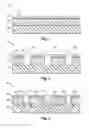
FIG. 2 is a schematic cross-sectional elevation view of the system of FIG. 1, showing the insulating material after etching the holes;
FIG. 3 is a schematic cross-sectional elevation view of the system of FIG. 1, showing the seed layer deposited over the insulating material and holes;
FIG. 4 is a schematic cross-sectional elevation view of the system of FIG. 1, showing the photo resist patterned on the seed layer;
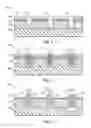
FIG. 5 is a schematic cross-sectional elevation view of the system of FIG. 1, showing the plating material plated into the holes; and
FIG. 6 is a schematic cross-sectional elevation view of the system of FIG. 1, showing the bump structures remaining after removing the photo resist material.
DETAILED DESCRIPTION OF THE PREFERRED EMBODIMENTS
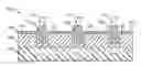
Reference will now be made to the drawings wherein like reference numerals identify similar structural features or aspects of the subject disclosure. For purposes of explanation and illustration, and not limitation, a partial view of an exemplary embodiment of a system in accordance with the disclosure is shown in FIG. 1 and is designated generally by reference character 100. Other embodiments of systems in accordance with the disclosure, or aspects thereof, are provided in FIGS. 2-7, as will be described. The systems and methods described herein can be used to provide improved bump structures, e.g., to accommodate smaller pixel pitch sizes in read-out integrated circuits (ROICs), photodiode arrays (PDAs), and smaller scale interconnections in other electronic assemblies.
System 100 is shown in FIG. 1 including an insulating material 102, e.g. of a polyimide or other suitable material, deposited on a wafer 104. A dielectric layer 106, e.g., of SiN or other suitable material, is deposited on the insulating material 102, and an initial layer of photo resist 108 is deposited on the dielectric layer 106. This initial structure can be used in a method of forming bump structures for interconnecting components. As shown in FIG. 2, the photo resist 108 is patterned, the dielectric layer 106 and insulating layer 102 are etched, e.g., by dry etching, to form holes 110 in the insulating material 102. The holes 110 provide a pattern 120 for bump structures 116 shown in FIG. 6. Dry etching the layer of insulating material 102 includes dry etching the dielectric layer 106.
The initial photo resist 108 is removed, and as shown in FIG. 3, a seed layer 112 is deposited on the insulating material 102 over the pattern, e.g., over the dielectric layer 106 and holes 110 in the insulating material 102. The seed layer 112 is deposited on the surface of the dielectric layer 106, e.g., on the top surface 128 of the hole pattern 120 of FIG. 2, on the sidewalls 130 of the holes 110, e.g., in direct contact with the insulating material 102, and on the bottom surface 132 of the holes 110 or base portion 126 of the pattern, e.g., in direct contact with the wafer 104. As shown in FIG. 4, the seed layer 112 is patterned with a second application of photo resist material 114. Seed layer 112 has the properties that allow for plating bump structures onto system 100 as explained below with reference to FIGS. 5-6.
With reference now to FIG. 5, with the photo resist material 114 patterned on seed layer 112, a plating material is plated over the seed layer 112 and the photo resist material 114 to form bump structures 116 in the pattern, i.e. bump structures made of the plating material in holes 110. It is contemplated that any suitable process besides plating can be used for forming the bump structures, e.g., evaporation techniques, without departing from the scope of this disclosure. The plating material is only deposited in the holes 110, so the bump structures 116 are isolated from one another electrically, and are spaced apart from one another by the insulating material 102. The plating material includes copper, indium, or any other suitable plating material, e.g., for electrical conductivity.
Referring now to FIG. 6, the method includes removing the photo resist material 114 after forming bump structures over the seed layer 112 and the photo resist material 114. Removing the photo resist material 114 can include leaving the bump structures 116 seated in a seat 122 of the seed layer 112. The remaining seed layer 112, i.e. the portions of seed layer 112 remaining in FIG. 6 from what is left after removing the portions of seed layer 112 shown in FIG. 5 but removed in FIG. 6, is recessed (as part of the removal of the photo resist material 114 of FIG. 5) below the top surface 134 of insulating material 102 (as oriented in FIG. 6, in other words the surface of insulating material 102 opposite wafer 104 and/or the bottoms surface 132 of holes 110 shown in FIG. 3), and below the surface 124 of the dielectric layer 106, to provide a gap 118 between each bump structure 116 and the insulating material 102 at the top of each hole 110. A portion of each bump structure 116 extends from the seat 122 and proud of top surface 128 of the hole pattern.
A focal plane array assembled from a PDA and ROIC as described above can define a plurality of pixels. The pixels can have a pitch size is less than 10 μm. The bump structures can each have a diameter less than 5 um. The bump structures can each have a height to diameter ratio of greater than 1:1.
The methods and systems of the present disclosure, as described above and shown in the drawings, provide for bump structures with superior properties including reduced bump size without short circuiting the bump structures in pressing. While the apparatus and methods of the subject disclosure have been shown and described with reference to preferred embodiments, those skilled in the art will readily appreciate that changes and/or modifications may be made thereto without departing from the scope of the subject disclosure.
Claims
What is claimed is:1. A method of forming bump structures for interconnecting components, comprising:
dry etching a layer of insulating material to create a pattern for bump structures;
depositing a seed layer on the insulating material over the pattern;
patterning the seed layer with a photo resist material; and
forming bump structures over the seed layer and the photo resist material with a plating material in the pattern, wherein the bump structures are isolated from one another.
2. A method as recited in claim 1, further comprising removing the photo resist material after forming the bump structures over the seed layer and the photo resist material.
3. A method as recited in claim 2, wherein removing the photo resist material includes leaving the bump structures seated in a seat of the seed layer, wherein the seed layer is recessed below the insulating material to provide a gap between the bump structures and the insulating material.
4. A method as recited in claim 1, wherein dry etching a layer of insulating material includes dry etching a dielectric layer deposited between the insulating material and an initial layer of photo resist material, patterning the initial layer of photo resist material, and dry etching the initial layer of photo resist material, the dielectric layer, and the insulating material to create the pattern for bump structures.
5. A method as recited in claim 4, wherein depositing the seed layer includes depositing the seed layer over the dielectric layer, over a wafer supporting the insulating material, and over the insulating material.
6. A method as recited in claim 5, wherein the seed layer is deposited on the wafer at a base portion of the pattern, wherein the seed layer is deposited on the dielectric layer at a surface of the pattern opposite of the base portion, and wherein the seed layer is deposited on the insulating material in sidewalls of the pattern.
7. A method as recited in claim 1, wherein the pattern includes holes for accommodating the bump structure, wherein forming the bump structures over the seed layer and the photo resist material with a plating material includes depositing plating material only in the holes.
8. A method as recited in claim 1, further comprising:
removing the photo resist material after forming the bump structures over the seed layer and the photo resist material, wherein removing the photo resist material includes leaving the bump structures seated in a seat of the seed layer, wherein the seed layer is recessed below the insulating material to provide a gap between the bump structures and the insulating material, with a portion of the bump structures extending from the seat proud of surface of the pattern; and
pressing the bump structures and laterally expanding the bump structures into the gap to keep the bump structures from electrically short circuiting with one another.
9. A method as recited in claim 1, wherein forming the bump structures over the seed layer and the photo resist material with a plating material includes plating with a plating material including at least one of copper or indium.
10. A system comprising:
a layer of insulating material with holes therein;
a seed layer seated within the holes, wherein the seed layer is recessed below a top surface of the insulating material that is opposite a bottom surface of the holes; and
a respective bump structure seated in the seed layer of each hole.
11. A system as recited in claim 10, wherein the bump structures are on one of a photodiode array (PDA) or a read-out integrated circuit (ROIC), and wherein the PDA and ROIC are joined together by the bump structures.
12. A system as recited in claim 11, wherein the PDA and ROIC define a plurality of pixels, wherein the plurality of pixels have a pitch size, wherein the pitch size is less than 10 μm.
13. A system as recited in claim 10, wherein the bump structures each have a diameter less than 5 um.
14. A system as recited in claim 10, wherein the bump structures each have a height to diameter ratio of greater than 1:1.
15. A system as recited in claim 10, wherein a portion of the bump structures extend from the seed layer proud of a top surface of the insulating material.
Images & Drawings included:
Sources:
- United States Patent and Trademark Office - verify current appl. status at the USPTO↗
Similar patent applications:
Recent applications in this class:
- » 20250048768 2025-02-06
SEMICONDUCTOR DEVICE, ELECTRONIC EQUIPMENT, AND WAFER - » 20250031475 2025-01-23
SEMICONDUCTOR CHIP, SOLID-STATE IMAGING DEVICE, AND ELECTRONIC EQUIPMENT - » 20250022901 2025-01-16
OPTICAL SEMICONDUCTOR PACKAGE AND METHOD FOR PRODUCING OPTICAL SEMICONDUCTOR PACKAGE - » 20250015116 2025-01-09
SEMICONDUCTOR DEVICE, APPARATUS, AND MANUFACTURING METHOD OF SEMICONDUCTOR DEVICE - » 20250006767 2025-01-02
OPTICAL SEMICONDUCTOR DEVICE WITH INTEGRATED VIAS IMPLEMENTING INTER-DIE CONNECTION - » 20250006766 2025-01-02
Stacking Single-Photon Avalanche Diodes and High Voltage Devices - » 20240421172 2024-12-19
TWO-WAY OPTICAL SENSOR PACKAGE AND A METHOD FOR FORMING THE SAME - » 20240413184 2024-12-12
RADIATION DETECTOR FOR POSITION-RESOLVED DETECTION OF RADIATION - » 20240405050 2024-12-05
SOLID-STATE IMAGING DEVICE, SOLID-STATE IMAGING DEVICE MANUFACTURING METHOD, AND ELECTRONIC DEVICE - » 20240405049 2024-12-05
SENSOR PACKAGE AND A METHOD FOR FORMING THE SAME
Recent applications for this Assignee:
- » 20240292074 2024-08-29
Neuromorphic compressive sensing in low-light environment - » 20240036176 2024-02-01
DETECTION PIXELS AND PIXEL SYSTEMS - » 20230333221 2023-10-19
TIME-OF-FLIGHT DISTANCE COMPENSATION THRESHOLD RAMP DRIVER - » 20230307481 2023-09-28
PHOTODETECTOR ARRAY (PDA) METALLIZATION - » 20230307398 2023-09-28
Hybridization bumps for fine pitch sensor arrays - » 20230305259 2023-09-28
SYSTEMS AND METHODS FOR ALIGNING IMAGING DEVICES - » 20230299223 2023-09-21
PHOTODIODE STRUCTURES - » 20230050990 2023-02-16
Visible-swir hyper spectral photodetectors with reduced dark current - » 20220079447 2022-03-17
VISUALIZATION FOR FLUORESCENT GUIDED IMAGING - » 20210288100 2021-09-16
Low capacitance photo detectors