Reflection structure for LED lamp
US20180119939A1
2018-05-03
15/310,765
2015-05-18
Abstract:
A reflection structure for an LED lamp contains: a substrate having an accommodation groove in which a plurality of cavities are defined and configured to accommodate multiple light-emitting diode (LED) chips respectively. The substrate also includes multiple partition ribs fixed in the accommodation groove of the substrate and configured to separate the plurality of cavities. Each of the multiple partition ribs separates any two adjacent of the plurality of cavities. Thereby, light from said each LED chip is reflected by said each partition rib and its radiation flux increases by way of a Nano-reflective material layer of said each partition rib, such that the substrate of the reflection structure protects said LED chip and dissipates heat of said LED chip effectively.
Interested in similar patents?
Get notified when new applications in this technology area are published.
Classification:
H01L33/483 » CPC further
Semiconductor devices with at least one potential-jump barrier or surface barrier specially adapted for light emission; Processes or apparatus specially adapted for the manufacture or treatment thereof or of parts thereof; Details thereof characterised by the semiconductor body packages Containers
F21Y2115/10 » CPC further
Light-generating elements of semiconductor light sources Light-emitting diodes [LED]
F21V7/0066 » CPC further
Reflectors for light sources specially adapted to cooperate with point like light sources; specially adapted to cooperate with light sources the shape of which is unspecified
H01L33/642 » CPC further
Semiconductor devices with at least one potential-jump barrier or surface barrier specially adapted for light emission; Processes or apparatus specially adapted for the manufacture or treatment thereof or of parts thereof; Details thereof characterised by the semiconductor body packages; Heat extraction or cooling elements characterized by the shape
H01L25/0753 » CPC further
Assemblies consisting of a plurality of individual semiconductor or other solid state devices ; Multistep manufacturing processes thereof all the devices being of a type provided for in the same subgroup of groups - , e.g. assemblies of rectifier diodes the devices not having separate containers the devices being of a type provided for in group the devices being arranged next to each other
F21V29/505 » CPC main
Protecting lighting devices from thermal damage; Cooling or heating arrangements specially adapted for lighting devices or systems; Cooling arrangements characterised by the adaptation for cooling of specific components of reflectors
H01L33/60 » CPC further
Semiconductor devices with at least one potential-jump barrier or surface barrier specially adapted for light emission; Processes or apparatus specially adapted for the manufacture or treatment thereof or of parts thereof; Details thereof characterised by the semiconductor body packages; Optical field-shaping elements Reflective elements
H01L33/48 IPC
Semiconductor devices with at least one potential-jump barrier or surface barrier specially adapted for light emission; Processes or apparatus specially adapted for the manufacture or treatment thereof or of parts thereof; Details thereof characterised by the semiconductor body packages
H01L25/075 IPC
Assemblies consisting of a plurality of individual semiconductor or other solid state devices ; Multistep manufacturing processes thereof all the devices being of a type provided for in the same subgroup of groups - , e.g. assemblies of rectifier diodes the devices not having separate containers the devices being of a type provided for in group
F21V7/00 IPC
Reflectors for light sources
F21V29/70 » CPC further
Protecting lighting devices from thermal damage; Cooling or heating arrangements specially adapted for lighting devices or systems; Cooling arrangements characterised by passive heat-dissipating elements, e.g. heat-sinks
H01L33/64 IPC
Semiconductor devices with at least one potential-jump barrier or surface barrier specially adapted for light emission; Processes or apparatus specially adapted for the manufacture or treatment thereof or of parts thereof; Details thereof characterised by the semiconductor body packages Heat extraction or cooling elements
Description
FIELD OF THE INVENTION
The present invention relates to a reflection structure for an LED lamp which protects multiple LED chips and dissipates heat of each LED chip effectively.
BACKGROUND OF THE INVENTION
A conventional LED chip contains light-emitting diode (LED) which is a two-lead semiconductor light source. It is a p-n junction diode, which emits light when activated.
In application, multiple light-emitting diode (LED) chips are die bonded on a printed circuit board (PCB) of an LED illumination device and are packaged. Alternatively, a single light-emitting diode (LED) chip is mounted and packaged on a support, and the support is fixed on the PCB, wherein a reflective lens is arranged on the LED illumination device so as to reflect and adjust the light from the LED chip.
The light from the LED chip impacts fluorescent powder so that the fluorescent powder emits fluorescence beams, but light loss of the fluorescence beams occurs.
Furthermore, lights between any two of the multiple LED chips offset with each other and reduce because of photon impact.
The present invention has arisen to mitigate and/or obviate the afore-described disadvantages.
SUMMARY OF THE INVENTION
The primary objective of the present invention is to provide a reflection structure for an LED lamp which protects multiple LED chips and dissipates heat of each LED chip effectively.
To obtain above-mentioned objective, a reflection structure for an LED lamp provided by the present invention contains: a substrate having an accommodation groove in which a plurality of cavities are defined and configured to accommodate multiple light-emitting diode (LED) chips respectively.
The substrate also includes multiple partition ribs fixed in the accommodation groove of the substrate and configured to separate the plurality of cavities, wherein each of the multiple partition ribs separates any two adjacent of the plurality of cavities.
Preferably, four peripheral walls of each of the plurality of cavities are defined by a side wall of the accommodation groove of the substrate and three of the multiple partition ribs or by four of the multiple partition ribs.
Preferably, an angle between each of the four peripheral walls of said each cavity and a top of said each cavity is 45 degrees.
Preferably, a cross section of said each partition rib is in a triangle shape.
Preferably, a cross section of said each partition rib is in an isosceles trapezoid shape.
Preferably, said each partition rib has a central support made of carbon fibers and has a reinforcement covering made of metal material. Thereby, said each partition rib is reinforced so as to protect each of the LED chips accommodated in each of the plurality cavities.
Preferably, said each partition rib further has a Nano-reflective material layer coated on the reinforcement covering so as to increase radiation flux of light of said each LED chip accommodated in said each cavity.
Accordingly, light from said each LED chip is reflected by said each partition rib and its radiation flux increases by way of a Nano-reflective material layer of said each partition rib, such that the substrate of the reflection structure protects said LED chip and dissipates heat of said LED chip effectively.
BRIEF DESCRIPTION OF THE DRAWINGS
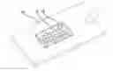
FIG. 1 is a perspective view showing the assembly of a reflection structure for an LED lamp according to a first embodiment of the present invention.
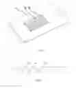
FIG. 2 is a cross sectional view showing the assembly of a part of the reflection structure for the LED lamp according to the first embodiment of the present invention.
FIG. 3 is a cross sectional view showing the assembly of a part of a reflection structure for an LED lamp according to a second embodiment of the present invention.
DETAILED DESCRIPTION OF THE PREFERRED EMBODIMENTS
With reference to FIG. 1, a reflection structure for a light-emitting diode (LED) lamp according to a first embodiment of the present invention comprises: a substrate 10 having an accommodation groove in which a plurality of cavities 11 are defined and configured to accommodate multiple light-emitting diode (LED) chips (not shown) respectively. The substrate 10 also includes multiple partition ribs 12 fixed in the accommodation groove thereof and configured to separate the plurality of cavities 11, for example, each of the multiple partition ribs 12 separates any two adjacent of the plurality of cavities 11.
The substrate 10 is in a rectangle shape or in a circle shape, and the plurality of cavities 11 are defined in a rectangular array in the substrate 10. Alternatively, the plurality of cavities 11 are defined in a circular array in the substrate 10.
Referring to FIG. 2, said each partition rib 12 has a central support 121 made of carbon fibers and has a reinforcement covering 122 made of metal material. Thereby, said each partition rib 12 is reinforced so as to protect each of the LED chips accommodated in each of the plurality cavities 11. Preferably, the central support 121 is made of carbon fibers and the reinforcement covering 122 is made of metal material, hence a heat dissipation of the substrate 10 enhances.
In addition, the multiple partition ribs 12 support other components mounted on the substrate 10.
Said each partition rib 12 further has a Nano-reflective material layer 123 coated on the reinforcement covering 122 so as to increase radiation flux of light of said each LED chip accommodated in said each cavity 11.
Four peripheral walls of said each cavity 11 are defined by a side wall of the accommodation groove of the substrate 10 and three of the multiple partition ribs 12 or by four of the multiple partition ribs 12, wherein an angle between each of the four peripheral walls of said each cavity 11 and a top of said each cavity 11 is 45 degrees, and a cross section of said each partition rib 12 is in a triangle shape. Preferably, the cross section of said each partition rib 12 is in an equilateral triangle shape so as to support and protect said each LED chip firmly.
As shown in FIG. 2, in a second embodiment, a cross section of said each partition rib 12 is in a trapezoid shape. Preferably, the cross section of said each partition rib 12 is in an isosceles trapezoid shape.
Thereby, the light from said each LED chip is reflected by said each partition rib and its radiation flux increases by way of the Nano-reflective material layer, and said each partition rib protects said each LED chip, hence the substrate of the reflection structure protects said LED chip and dissipates heat of said LED chip effectively.
While the preferred embodiments of the invention have been set forth for the purpose of disclosure, modifications of the disclosed embodiments of the invention as well as other embodiments thereof may occur to those skilled in the art. Accordingly, the appended claims are intended to cover all embodiments which do not depart from the spirit and scope of the invention.
Claims
What is claimed is:1. A reflection structure for an LED lamp comprising:
a substrate having an accommodation groove in which a plurality of cavities are defined and configured to accommodate multiple light-emitting diode (LED) chips respectively,
the substrate also including multiple partition ribs fixed in the accommodation groove of the substrate and configured to separate the plurality of cavities;
wherein each of the multiple partition ribs separates any two adjacent of the plurality of cavities.
2. The reflection structure as claimed in claim 1, wherein said each partition rib has a central support made of carbon fibers and has a reinforcement covering made of metal material.
3. The reflection structure as claimed in claim 2, wherein four peripheral walls of each of the plurality of cavities are defined by a side wall of the accommodation groove of the substrate and three of the multiple partition ribs or by four of the multiple partition ribs.
4. The reflection structure as claimed in claim 3, wherein an angle between each of the four peripheral walls of said each cavity and a top of said each cavity is 45 degrees.
5. The reflection structure as claimed in claim 4, wherein a cross section of said each partition rib is in a triangle shape.
6. The reflection structure as claimed in claim 4, wherein a cross section of said each partition rib is in an isosceles trapezoid shape.
Images & Drawings included:

Sources:
- United States Patent and Trademark Office - verify current appl. status at the USPTO↗
Similar patent applications:
Recent applications in this class:
- » 20200309361 2020-10-01
Semi-transparent sign temperature protection - » 20190368715 2019-12-05
Lamp unit - » 20190242567 2019-08-08
Variable area microjets to cool digital micromirror devices - » 20190242566 2019-08-08
Synthetic jets to cool digital micromirror devices - » 20170292690 2017-10-12
HEAT DISSIPATING REFLECTORS FOR LED LUMINAIRES - » 20160258610 2016-09-08
ILLUMINATING DEVICE - » 20120319554 2012-12-20
Electric lamp having reflector for transferring heat from light source - » 20120300455 2012-11-29
Illumination Device - » 20120300453 2012-11-29
Omni reflective optics for wide angle emission LED light bulb - » 20120268942 2012-10-25
Reflector lamp with improved heat dissipation and reduced weight