Electrical and optical via connections on a same chip
US20180158967A1
2018-06-07
15/886,927
2018-02-02
✅ Patent granted
US 10,403,772 B2
2019-09-03
-
-
Ellen E Kim
Michael Le Strange | Andrew M. Calderon | Roberts Mlotkowski Safran Cole & Calderon, P.C.
2038-02-02
Abstract:
The present disclosure relates to semiconductor structures and, more particularly, to electrical and optical via connections on a same chip and methods of manufacture. The structure includes an optical through substrate via (TSV) comprising an optical material filling the TSV. The structure further includes an electrical TSV which includes a liner of the optical material and a conductive material filling remaining portions of the electrical TSV.
Inventors:
- Geng WANG 162 🇺🇸 Stormville, NY, United States
- Kangguo CHENG 2,623 🇺🇸 Schenectady, NY, United States
- Chengwen Pei 149 🇺🇸 Danbury, CT, United States
- Joseph Ervin 43 🇺🇸 Wappingers Falls, NY, United States
- Juntao Li 593 🇺🇸 Cohoes, NY, United States
- Joseph Ervin 1 🇺🇸 Wappinger Falls, NY, United States
Assignee:
- GLOBALFOUNDRIES Inc. 5,848 Grand Cayman, Cayman Islands
Applicant:
Interested in similar patents?
Get notified when new applications in this technology area are published.
Classification:
H01L31/02327 » CPC main
Semiconductor devices sensitive to infra-red radiation, light, electromagnetic radiation of shorter wavelength or corpuscular radiation and specially adapted either for the conversion of the energy of such radiation into electrical energy or for the control of electrical energy by such radiation; Processes or apparatus specially adapted for the manufacture or treatment thereof or of parts thereof; Details thereof; Details; Optical elements or arrangements associated with the device the optical elements being integrated or being directly associated to the device, e.g. back reflectors
H01L31/02 IPC
Semiconductor devices sensitive to infra-red radiation, light, electromagnetic radiation of shorter wavelength or corpuscular radiation and specially adapted either for the conversion of the energy of such radiation into electrical energy or for the control of electrical energy by such radiation; Processes or apparatus specially adapted for the manufacture or treatment thereof or of parts thereof; Details thereof Details
G02B6/428 » CPC further
Light guides; Coupling light guides; Coupling light guides with opto-electronic elements; Packages, e.g. shape, construction, internal or external details; Electrical aspects containing printed circuit boards [PCB]
H01L23/481 » CPC further
Details of semiconductor or other solid state devices; Arrangements for conducting electric current to or from the solid state body in operation, e.g. leads, terminal arrangements ; Selection of materials therefor Internal lead connections, e.g. via connections, feedthrough structures
H01L31/02005 » CPC further
Semiconductor devices sensitive to infra-red radiation, light, electromagnetic radiation of shorter wavelength or corpuscular radiation and specially adapted either for the conversion of the energy of such radiation into electrical energy or for the control of electrical energy by such radiation; Processes or apparatus specially adapted for the manufacture or treatment thereof or of parts thereof; Details thereof; Details; Arrangements for conducting electric current to or from the device in operations for device characterised by at least one potential jump barrier or surface barrier
G02B2006/12061 » CPC further
Light guides of the optical waveguide type of the integrated circuit kind; Materials Silicon
G02B6/12 IPC
Light guides of the optical waveguide type of the integrated circuit kind
H01L31/0232 IPC
Semiconductor devices sensitive to infra-red radiation, light, electromagnetic radiation of shorter wavelength or corpuscular radiation and specially adapted either for the conversion of the energy of such radiation into electrical energy or for the control of electrical energy by such radiation; Processes or apparatus specially adapted for the manufacture or treatment thereof or of parts thereof; Details thereof; Details Optical elements or arrangements associated with the device
H01L23/48 IPC
Details of semiconductor or other solid state devices Arrangements for conducting electric current to or from the solid state body in operation, e.g. leads, terminal arrangements ; Selection of materials therefor
G02B6/42 IPC
Light guides; Coupling light guides Coupling light guides with opto-electronic elements
H01L21/76898 » CPC further
Processes or apparatus adapted for the manufacture or treatment of semiconductor or solid state devices or of parts thereof; Manufacture or treatment of devices consisting of a plurality of solid state components formed in or on a common substrate or of parts thereof; Manufacture of integrated circuit devices or of parts thereof; Manufacture of specific parts of devices defined in group; Applying interconnections to be used for carrying current between separate components within a device comprising conductors and dielectrics formed through a semiconductor substrate
H01L21/768 IPC
Processes or apparatus adapted for the manufacture or treatment of semiconductor or solid state devices or of parts thereof; Manufacture or treatment of devices consisting of a plurality of solid state components formed in or on a common substrate or of parts thereof; Manufacture of integrated circuit devices or of parts thereof; Manufacture of specific parts of devices defined in group Applying interconnections to be used for carrying current between separate components within a device comprising conductors and dielectrics
G02B6/43 » CPC further
Light guides; Coupling light guides; Coupling light guides with opto-electronic elements Arrangements comprising a plurality of opto-electronic elements and associated optical interconnections
G02B2006/12123 » CPC further
Light guides of the optical waveguide type of the integrated circuit kind; Constructional arrangements Diode
G02B6/122 » CPC further
Light guides of the optical waveguide type of the integrated circuit kind Basic optical elements, e.g. light-guiding paths
Description
FIELD OF THE INVENTION
The present disclosure relates to semiconductor structures and, more particularly, to electrical and optical via connections on a same chip and methods of manufacture.
BACKGROUND
Integrated optical and electrical through silicon vias (TSVs) are critical for multifunctional systems on chip (MSoC), for example, having optical circuits and electrical circuits on a single chip. The integration of the optical and electrical TSVs is a great challenge, though. Specifically, current processes require multiple mask sets and complex processes, leading to overall low yields and higher manufacturing costs.
SUMMARY
In an aspect of the disclosure, a structure comprises: an optical through substrate via (TSV) comprising an optical material filling the TSV; and an electrical TSV comprising a liner of the optical material and a conductive material filling remaining portions of the electrical TSV.
In an aspect of the disclosure, a structure comprises: an optical through silicon via (TSV) having an annular shape and comprising an optical material; an electrical TSV having a via shape and comprising a liner of the optical material and a conductive material filling remaining portions of the electrical TSV; an airgap formed in the silicon and in alignment with the optical TSV; and a photodetector in alignment with the airgap and the optical TSV.
In an aspect of the disclosure, a method comprises: forming an annular via and a via shaped via in a substrate using a same lithography process; filling the annular via with optical material while forming a liner on sidewalls of a electrical TSV via with the optical material, in a same deposition process; filling remaining portions of the electrical TSV via with conductive material; removing a back side of the substrate to form an annular optical TSV comprising the annular via with the optical material and an electrical via from the electrical TSV via with the optical material and the conductive material; and forming an airgap in the substrate in alignment with the annular optical TSV.
BRIEF DESCRIPTION OF THE DRAWINGS
The present disclosure is described in the detailed description which follows, in reference to the noted plurality of drawings by way of non-limiting examples of exemplary embodiments of the present disclosure.
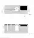
FIG. 1A shows a top down view of a structure and respective fabrication processes in accordance with aspects of the present disclosure.
FIG. 1B shows a cross-sectional view of the structure of FIG. 1A, along line A-A.
FIG. 2 shows an optical via filled with optical material and an electrical via lined with the optical material and respective fabrication processes in accordance with aspects of the present disclosure.
FIG. 3 shows the electrical via filled with conductive material and respective fabrication processes in accordance with aspects of the present disclosure.
FIG. 4 shows a handle wafer attached to the structure of FIG. 3 and respective fabrication processes in accordance with aspects of the present disclosure.
FIG. 5 shows a thinned wafer with the filled optical via and electrical via and respective fabrication processes in accordance with aspects of the present disclosure.
FIG. 6A shows a top down view of an optical through silicon via and an electrical through silicon via and respective fabrication processes in accordance with aspects of the present disclosure.
FIG. 6B shows a cross-sectional view of the structure of FIG. 6A, along line A-A.
FIG. 7 shows a cross-sectional view of a final structure and respective fabrication processes in accordance with aspects of the present disclosure.
DETAILED DESCRIPTION
The present disclosure relates to semiconductor structures and, more particularly, to electrical and optical via connections on a same chip and methods of manufacture. More specifically, the present disclosure provides a method to fabricate optical TSVs and electrical TSVs on a single chip, resulting in an advantageously designed structure. In embodiments, for example, an annular-shape optical TSV and via-shape electric TSV are formed simultaneously on a single chip, enabling a mask-free process. The annular-shape optical TSV and via-shape electric TSV can be formed with other devices on the same chip.
The electrical and optical via connections of the present disclosure can be manufactured in a number of ways using a number of different tools. In general, though, the methodologies and tools are used to form structures with dimensions in the micrometer and nanometer scale. The methodologies, i.e., technologies, employed to manufacture the electrical and optical via connections of the present disclosure have been adopted from integrated circuit (IC) technology. For example, the structures are built on wafers and are realized in films of material patterned by photolithographic processes on the top of a wafer. In particular, the fabrication of the electrical and optical via connections uses three basic building blocks: (i) deposition of thin films of material on a substrate, (ii) applying a patterned mask on top of the films by photolithographic imaging, and (iii) etching the films selectively to the mask.
FIG. 1A shows a top down view of a structure and respective fabrication processes in accordance with aspects of the present disclosure. FIG. 1B shows a cross-sectional view of the structure of FIG. 1A, along line A-A. It should be noted that the top down view of FIG. 1A does not include a mask, in order to show the different devices/circuits formed on or within the substrate.
More specifically and referring to both FIGS. 1A and 1B, the structure 5 includes a substrate 10 with a plurality of devices 14. In embodiments, the substrate 10 can be a semiconductor material such as, for example, Si; although other substrates are contemplated herein, e.g., SiGe, etc. The devices 14 can be any active or passive devices formed using conventional CMOS process. For example, the devices 14 can be logic devices, analog devices, processors, resistors, capacitors, etc., or other front end of the line (FEOL) or back end of the line (BEOL) devices.
Still referring to FIGS. 1A and 1B, an optical via 16 and an electrical via 18 can be formed in the substrate 10. In embodiments, the optical via 16 is preferably an annular shaped via with a via width dimension of “d1” and a width of the core portion of the annular shape, e.g., circumferential dimension, “d2”. The electrical via 18 has a width (diameter) of “D1”, where D1>d1. In embodiments, the dimension “d1” can be about 50 nm to 2 micron and dimension “d2” can be about 100 nm to about 5 micron or more as needed; although other dimensions for d1 and d2 are also contemplated herein. On the other hand, dimension “D1” is preferably greater than 300 nm and more preferably ranges from about 1 micron to about 10 microns, or more as needed. Although the electrical via 18 is shown with a circular cross-section, other shapes are also contemplated herein.
In embodiments, the optical via 16 and the electrical via 18 can be fabricated with a single mask 12, e.g., using mask 12 with a single lithography step. For example, in embodiments, the mask 12 can be an oxide material, nitride material, carbide, etc. In more specific embodiments, a resist formed over the mask 12 can be exposed to energy (e.g., light) to form one or more openings (e.g., patterns) which correspond to the dimensions “d1” and “D1”. An etching process, e.g., reactive ion etching (RIE), can be performed through the openings, with a chemistry selective to the mask 12 and underlying semiconductor material 10. The etching process will form openings in the semiconductor material 10 partly through the depth thereof. The resist is then removed using conventional stripants, e.g., oxygen ashing.
In FIG. 2, a deposition process is performed to fill the optical via 16 with optical material 20, which will also form a liner 20a on sidewalls of the electrical via 18. It should be understood by those of skill in the art that due to the wider dimension “D1” of the electrical via 18, the deposited optical material will not pinch off the opening of the electrical via 18; instead, in embodiments, the optical material will form a liner 20a of a thickness approximately equaling the dimension “d1” of the optical via 16, e.g., about 50 nm to about 2 micron in thickness. In embodiments, the deposition process is a chemical vapor deposition (CVD) process using, e.g., an optical material. For example, the optical material is a transparent material such as an oxide material, with the CVD process being an oxide flow. Any residual material formed on the mask 12 can be removed by a chemical mechanical process (CMP).
As shown in FIG. 3, a conductive material 22 fills in the remaining portion of the electrical via 18. In embodiments, the conductive material 22 can be a metal material. In more specific embodiments, the conductive material 22 can be tungsten, copper, aluminum, titanium, cobalt or other metal or metal alloy materials. The conductive material 22 can be deposited by a conventional CVD process, followed by a CMP process to remove any residual material from the mask 12.
Referring to FIG. 4, the mask is removed and a handle wafer or carrier 24 is attached to the substrate 10. In embodiments, the mask can be removed during the above described CMP process, e.g., the CMP process which is used to remove any residual conductive material. The handle wafer or carrier 24 can be a Si mandrel bonded to the substrate 10 via an oxide-oxide bond. In alternative embodiments, the handle wafer or carrier 24 can be attached to the substrate 10 by an adhesive or an organic glue, as examples known to those of skill in the art such that further explanation is not required for an understanding of the processes described herein.
In FIG. 5, the back side of the substrate 10 is removed to expose the conductive material 22 as well as the transparent material 20, 20a. In this way, an optical TSV 26 and electrical TSV 28 are now fully formed within the substrate 10 on a same chip, while being able to reduce masking steps, e.g., reducing complexity of the fabrication process and resultant manufacturing costs. In embodiments, the optical TSV 26 is an annular shaped optical TSV and the electrical TSV 28 can be any via shape. The back side of the substrate 10 can be removed by known processes such as, for example, etching, grinding, polishing or any combination of such techniques.
FIG. 6A shows a top down view of the optical TSV 26 and electrical TSV 28 and respective fabrication processes in accordance with aspects of the present disclosure; whereas, FIG. 6B shows a cross-sectional view of the structure of FIG. 6A, along line A-A. In these representative figures, it is shown that the optical TSV 26 includes a core of the substrate material 10. Also, the electrical TSV 28 includes a liner of the optical material, e.g., dielectric material to insulate the conductive material 24 from the substrate 10. In embodiments, the handle wafer is also removed using known processes.
FIG. 7 shows a cross-sectional view of a final structure and respective fabrication processes in accordance with aspects of the present disclosure. More specifically, the optical TSV 26 is shown to be attached to a substrate 10′ having a photodetector 30. In more specific embodiments, the photodetector 30 is aligned with the optical TSV 26, and more particularly, with an airgap 32 formed in the substrate 10 aligned with the optical TSV 26. In embodiments, the airgap 32 is formed by conventional lithography and etching processes as already described herein. More specifically, in embodiments, the airgap 32 can be formed in the substrate 10, in alignment with, e.g., overlapping, the optical TSV 26, using conventional lithography and etching processes, prior to the bonding of the substrates 10, 10′.
In embodiments, the airgap 32 has a depth ranging from about 100 nm to about 10 microns. Moreover, the airgap 32 spans the core of the annular shaped optical TSV 26 and overlaps with the optical material filling the optical TSV 26. As should be understood by those of skill in the art, the core of the annular shaped optical TSV 26 is composed of the substrate material 10, e.g., silicon.
The substrates 10, 10′ can be bonded together using an oxide-oxide bond. In embodiments, the electrical TSV 28 formed in the substrate 10 will also be aligned with and in electrical contact with an electrical TSV 28′ formed in the substrate 10′. In embodiments, additional devices 14 can also be formed in the substrate 10′, similar to that which was already described herein.
The method(s) as described above is used in the fabrication of integrated circuit chips. The resulting integrated circuit chips can be distributed by the fabricator in raw wafer form (that is, as a single wafer that has multiple unpackaged chips), as a bare die, or in a packaged form. In the latter case the chip is mounted in a single chip package (such as a plastic carrier, with leads that are affixed to a motherboard or other higher level carrier) or in a multichip package (such as a ceramic carrier that has either or both surface interconnections or buried interconnections). In any case the chip is then integrated with other chips, discrete circuit elements, and/or other signal processing devices as part of either (a) an intermediate product, such as a motherboard, or (b) an end product. The end product can be any product that includes integrated circuit chips, ranging from toys and other low-end applications to advanced computer products having a display, a keyboard or other input device, and a central processor.
The descriptions of the various embodiments of the present disclosure have been presented for purposes of illustration, but are not intended to be exhaustive or limited to the embodiments disclosed. Many modifications and variations will be apparent to those of ordinary skill in the art without departing from the scope and spirit of the described embodiments. The terminology used herein was chosen to best explain the principles of the embodiments, the practical application or technical improvement over technologies found in the marketplace, or to enable others of ordinary skill in the art to understand the embodiments disclosed herein.
Claims
What is claimed:1. A method, comprising:
forming an optical through substrate via (TSV) in a substrate comprising:
forming an annular via around a core portion comprised of a portion of the substrate, wherein the annular via has a via width “d1” between an inner wall of the annular via adjacent to the core portion and an outer wall of the annular via spaced apart from the core portion, and wherein a circumferential dimension of the core portion is “d2”; and
filling an optical material in the annular via; and
forming an electrical TSV in the substrate comprising:
forming a via in the substrate, spaced apart from the annular via;
forming a liner of the optical material on sidewalls of the via; and
forming an electrically conductive material in remaining portions of the via,
wherein the electrical TSV has a diameter of “D1”, where D1>d1.
2. The method of claim 1, wherein the substrate is silicon and the optical TSV and the electrical TSV are through the silicon vias.
3. The method of claim 1, wherein the optical material is oxide material.
4. The method of claim 1, wherein the electrical TSV is via shape.
5. The method of claim 4, wherein a width dimension of the optical TSV is smaller than a width dimension of the electrical TSV.
6. The method of claim 4, wherein the optical TSV and the electrical TSV extend entirely through the substrate.
7. The method of claim 4, further comprising forming at least one additional device in the substrate spaced apart from the optical TSV and the electrical TSV.
8. The method of claim 1, further comprising forming an airgap in the substrate in alignment with the optical TSV.
9. The method of claim 8, wherein the airgap is formed by recessing the optical material and the core portion in the substrate.
10. The method of claim 9, further comprising forming a photodetector in alignment with the airgap and the optical TSV.
11. The method of claim 10, wherein the airgap spans the core portion and overlaps with the optical material filling the TSV of the optical TSV.
12. The method of claim 11, wherein the photodetector is provided in another substrate which is bonded to the substrate having the optical TSV.
13. The method of claim 12, further comprising bonding the another substrate having the photodetector to the substrate having the optical TSV using an oxide-oxide bond.
14. The method of claim 13, wherein the another substrate includes an electrical TSV which electrically contacts the electrical TSV of the substrate having the optical TSV.
Images & Drawings included:


Sources:
- United States Patent and Trademark Office - verify current appl. status at the USPTO↗
Similar patent applications:
Recent applications in this class:
- » 20250063851 2025-02-20
Non-Rectangular Germanium Photodetector with Angled Input Waveguide - » 20250040291 2025-01-30
PHOTODETECTOR - » 20250015211 2025-01-09
PHOTODETECTOR - » 20240405136 2024-12-05
SEMICONDUCTOR LIGHT RECEIVING DEVICE - » 20240405135 2024-12-05
Electromagnetic Radiation Detectors with Lattice-Matched Epitaxial Anti-Reflection Structures - » 20240387757 2024-11-21
Integrated Photodetector - » 20240372018 2024-11-07
SEMICONDUCTOR DEVICE COMPRISING A PHOTODETECTOR WITH REDUCED DARK CURRENT - » 20240363772 2024-10-31
APPARATUS AND METHOD FOR ABSORBING ELECTROMAGNETIC RADIATION, SYSTEM FOR USE IN AN IMAGE SENSOR, AS WELL AS A METHOD FOR MANUFACTURING AN APPARATUS FOR ABSORBING ELECTROMAGNETIC RADIATION - » 20240347652 2024-10-17
PHOTODETECTORS WITH A LIGHT-ABSORBING LAYER AT LEAST PARTIALLY WRAPPED ABOUT A WAVEGUIDE CORE - » 20240332438 2024-10-03
WAVEGUIDE-TYPE LIGHT-RECEIVING ELEMENT, WAVEGUIDE-TYPE LIGHT-RECEIVING ELEMENT ARRAY, AND METHOD FOR MANUFACTURING WAVEGUIDE-TYPE LIGHT-RECEIVING ELEMENT
Recent applications for this Assignee:
- » 20220238386 2022-07-28
METHODS, APPARATUS, AND MANUFACTURING SYSTEM FOR SELF-ALIGNED PATTERNING OF A VERTICAL TRANSISTOR - » 20220200636 2022-06-23
Multiband receivers for millimeter wave devices - » 20220085994 2022-03-17
Public-private encryption key generation using Pcell parameter values and on-chip physically unclonable function values - » 20210066503 2021-03-04
Body-contacted field effect transistors configured for test and methods - » 20210063531 2021-03-04
Transmitter unit suitable for millimeter wave devices - » 20210057592 2021-02-25
Semiconductor detectors with butt-end coupled waveguide and method of forming the same - » 20210043727 2021-02-11
Gate-all-around field effect transistors with robust inner spacers and methods - » 20210027005 2021-01-28
Method, apparatus and system for wide metal line for SADP routing - » 20210005601 2021-01-07
Fin-type field effect transistor with reduced fin bulge and method - » 20210005454 2021-01-07
Metal on metal multiple patterning