Digital to analog converter and display panel having digital to analog converter
US20180164623A1
2018-06-14
15/128,379
2016-07-08
✅ Patent granted
US 10,185,166 B2
2019-01-22
WO; PCT/CN2016/089364; 20160708
WO; WO2017/201826; 20171130
Tony Davis
Mintz Levin Cohn Ferris Glovsky and Popeo, P.C. | Kongsik Kim | Jhongwoo Jay Peck
2036-12-23
Abstract:
A digital to analog converter includes N lines of transistors. A number of each rear line of transistors is equal to a half of a number of each adjacent front line of transistors. Each transistor includes a conducting terminal, an input terminal, and an output terminal. In any two adjacent lines of transistors, input terminals of the first transistors and input terminals of the second transistors of the rear line are connected to output terminals of the first transistors of a front line respectively. Output terminals of the second transistors of the front line are connected to output terminals of the first transistors of the front line. Output terminals of the second transistors of the rear line of transistors are connected to output terminals of the first transistor of the rear line of transistors. Conducting terminals of each line of transistors are connected to each other.
Assignee:
- Shenzhen China Star Optoelectronics Technology Co Ltd. 3,202 🇨🇳 Shenzhen, Guangdong, China
- SHENZHEN CHINA STAR OPTOELECTRONICS TECHNOLOGY CO., LTD. 1,397 🇨🇳 Shenzhen, China
Applicant:
Interested in similar patents?
Get notified when new applications in this technology area are published.
Classification:
G02F1/13306 » CPC main
Devices or arrangements for the control of the intensity, colour, phase, polarisation or direction of light arriving from an independent light source, e.g. switching, gating or modulating; Non-linear optics for the control of the intensity, phase, polarisation or colour based on liquid crystals, e.g. single liquid crystal display cells; Constructional arrangements; Operation of liquid crystal cells; Circuit arrangements Circuit arrangements or driving methods for the control of single liquid crystal cells
H03M1/66 » CPC further
Analogue/digital conversion; Digital/analogue conversion Digital/analogue converters
G09G3/3685 » CPC further
Control arrangements or circuits, of interest only in connection with visual indicators other than cathode-ray tubes for presentation of an assembly of a number of characters, e.g. a page, by composing the assembly by combination of individual elements arranged in a matrix no fixed position being assigned to or needed to be assigned to the individual characters or partial characters by control of light from an independent source using liquid crystals; Control of matrices with row and column drivers Details of drivers for data electrodes
G09G2310/027 » CPC further
Command of the display device; Addressing, scanning or driving the display screen or processing steps related thereto; Details of driving circuits Details of drivers for data electrodes, the drivers handling digital grey scale data, e.g. use of D/A converters
G02F1/133 IPC
Devices or arrangements for the control of the intensity, colour, phase, polarisation or direction of light arriving from an independent light source, e.g. switching, gating or modulating; Non-linear optics for the control of the intensity, phase, polarisation or colour based on liquid crystals, e.g. single liquid crystal display cells Constructional arrangements; Operation of liquid crystal cells; Circuit arrangements
G09G3/36 » CPC further
Control arrangements or circuits, of interest only in connection with visual indicators other than cathode-ray tubes for presentation of an assembly of a number of characters, e.g. a page, by composing the assembly by combination of individual elements arranged in a matrix no fixed position being assigned to or needed to be assigned to the individual characters or partial characters by control of light from an independent source using liquid crystals
H03M1/76 » CPC further
Analogue/digital conversion; Digital/analogue conversion; Digital/analogue converters; Simultaneous conversion using switching tree
G09G3/3648 » CPC further
Control arrangements or circuits, of interest only in connection with visual indicators other than cathode-ray tubes for presentation of an assembly of a number of characters, e.g. a page, by composing the assembly by combination of individual elements arranged in a matrix no fixed position being assigned to or needed to be assigned to the individual characters or partial characters by control of light from an independent source using liquid crystals; Control of matrices with row and column drivers using an active matrix
Description
BACKGROUND OF THE INVENTION
1. Field of the Invention
The present invention relates to a digital to analog converting field, especially relates to a digital to analog converter and a display panel having the digital to analog converter.
2. Description of Related Art
Liquid crystal display televisions, which have a small size, a light weight, and an excellent display effect, are very popular to people. Resources become poor with the development of economy. Thus, it is a problem how to design liquid crystal displays with excellent display effect by using less resources.
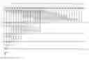
A circuit drive system of a display panel (such as a liquid crystal display) includes a data control module, a source converting module, a Gamma voltage drive module, a data drive module, and a scanning drive module. Wherein the cost of the data control module in the entire circuit drive system. The digital to analog converter of the data drive module includes a plurality of transistors. Referring to FIG. 1, a 5-bit digital to analog converter includes five lines of transistors. Each line of transistors includes 32 transistors. The converter has a complex structure with a high cost because of so many transistors.
Thus, to solve above technical problem, a digital to analog converter and a display panel having the digital to analog converter are required.
SUMMARY OF THE INVENTION
In order to overcome the deficiency of the related art, the purpose of the present disclosure is to provide a digital to analog converter and a display panel having the digital to analog converter.
In order to achieve the above purpose, a technology solution provided by the embodiment of the present disclosure is:
A digital to analog converter includes N lines of transistors. A number of each rear line of transistors is equal to a half of a number of each adjacent front line of transistors. A number of the N lines of transistors is equal to
∑ 1 N 2 M .
M, N is natural numbers, N is greater than 1, and M is no less than 1 and not greater than N. Each transistor includes a conducting terminal, an input terminal, and an output terminal; a number of a first line of transistors is 2N, and a number of a last line of transistors is 2. Input terminals of the first line of transistors are configured to receive 2N different voltage signals. Each line of transistors includes a half of first transistors and a half of second transistors. A conducting level of the half of first transistors is different from a conducting level of the half of second transistors. In any two adjacent lines of transistors, input terminals of the first transistors and input terminals of the second transistors of the rear line are connected to output terminals of the first transistors of a front line respectively. Output terminals of the second transistors of the front line are connected to output terminals of the first transistors of the front line, and output terminals of the second transistors of the rear line of transistors are connected to output terminals of the first transistor of the rear line of transistors. Conducting terminals of each line of transistors are connected to each other and receiving a high level signal or a low level signal indicating a digital signal; and output terminals of the two transistors of the last line of transistors are connected to each other and configured to output a converted analog signal.
As a further improvement of the present disclosure, the transistors are field effect transistors, the conducting terminal is a gate of the field effect transistor, the input terminal is a drain of the field effect transistor, and the output terminal is a source of the field effect transistor.
As a further improvement of the present disclosure, the first transistor is an N channel field effect transistor, and the second transistor is a P channel field effect transistor.
As a further improvement of the present disclosure, the transistors are triode transistors, the conducting terminal is a base of the triode transistor, the input terminal is a collector of the triode transistor, and the output terminal is an emitter of the triode transistor.
As a further improvement of the present disclosure, the conducting terminal of the first transistor is configured to receive a low level signal to be conducted, and the conducting terminal of the second transistor is configured to receive a high level signal to be conducted.
Correspondingly, a display panel includes the above digital to analog converter.
The benefit of the present disclosure is: the digital to analog converter of the present disclosure including a plurality of lines of transistors; the number of the rear line of transistors being equal to the number of the adjacent front line of transistors; the digital to analog converter having a simple structure and less transistors for converting digital signals, thereby reducing the cost of the converter.
BRIEF DESCRIPTION OF THE DRAWINGS
FIG. 1 is a circuit diagram showing the digital to analog converter of the related art.
FIG. 2 is a circuit diagram showing the digital to analog converter according to an embodiment of the present disclosure.
DETAILED DESCRIPTION OF THE PREFERRED EMBODIMENT
The following content combines with the figures and the embodiments for describing the present invention in detail. It is obvious that the following embodiments are only some embodiments of the present invention. For the person of ordinary skill in the art without creative effort, the other embodiments obtained thereby are still covered by the present invention.
Referring to FIG. 1, a display panel (now shown) includes a digital to analog converter. The digital to analog converter includes N lines of transistors. The number of each line of transistors is arranged in a way that the number of a rear line of transistors is a half of the number of a front line of transistors. The number of the N lines of transistors is
∑ 1 N 2 M .
M, N are natural numbers, N is greater than 1, and M is no less than 1 and not greater than N. Each transistor includes a conducting terminal, an input terminal, and an output terminal. The number of the first line of transistors is 2N, and the number of a last line of transistors is 2. The display panel further includes 2N different voltage signals (V1, V2, V3, . . . V32). The input terminals of the first line of transistors is used for receiving 2N different voltage signals (V1, V2, V3, . . . V32).
Each line of transistors comprises a half of first transistors 101 and a half of second transistors 102. The conducting level of the conducting terminal of the first transistor 101 is opposed to the conducting level of the conducting terminal of the second transistor 102. In the embodiment, the conducting terminal of the first transistor 101 is used for receiving a low level to be conducted, and the conducting terminal of the second transistor 102 is used for receiving a high level to be conducted. In any two adjacent lines of transistors, input terminals of the first transistors and input terminals of the second transistors of the rear line are connected to output terminals of the first transistors of a front line respectively, output terminals of the second transistors of the front line are connected to output terminals of the first transistors of the front line, and output terminals of the second transistors of the rear line of transistors are connected to output terminals of the first transistor of the rear line of transistors. The conducting terminals of each line of transistors are connected to each other and receive a high level signal or a low level signal (D1, D1, D2, D3, D4) indicating a digital signal. The output terminals of the two transistors of the last line of transistors are connected to each other and used for outputting a converted analog signal Vout.
In the present embodiment, the transistors are field effect transistors. The conducting terminal is a gate of the field effect transistor, the input terminal is a drain of the field effect transistor, and the output terminal is a source of the field effect transistor.
In use, when the signals D0, D1, D2, D3, D4 are different high or low level signals indicating data signal, the transistor are be conducted to enable the voltage value of the converted analog signal Vout to be equal to the voltage value of one of the voltage signals V1, . . . V32. For example, when the signal D3 of the signals D0, D1, D2, D3, D4 is low level and others are high levels, Vout is equal to V24.
In another embodiment, the transistors are the transistors are triode transistors, the conducting terminal is a base of the triode transistor, the input terminal is a collector of the triode transistor, and the output terminal is an emitter of the triode transistor.
The number of each line of transistors is arranged in a way that the number of a rear line of transistors is a half of the number of a front line of transistors in the digital to analog converter of the present disclosure, the digital to analog converter has a simple structure and less transistors for converting the same digital signals relative to the converter of the prior art, thereby reducing the cost of the converter.
For the person skilled in the art, obviously, the present invention is not limited to the detail of the above exemplary embodiment. Besides, without deviating the spirit and the basic feature of the present invention, other specific forms can also achieve the present invention. Therefore, no matter from what point of view, the embodiments should be deemed to be exemplary, not limited. The range of the present invention is limited by the claims not by the above description. Accordingly, the embodiments are used to include all variation in the range of the claims and the equivalent requirements of the claims. It should not regard any reference signs in the claims as a limitation to the claims.
Besides, it can be understood that, although the present disclosure is describe according to the embodiments, each embodiment does not include only on dependent technology solution. The description of the present disclosure is only for clarity. The person skilled in the art should regard the present disclosure as an entirety. Technology solutions in the embodiments can be adequately combined to form other embodiments that can be understood by the person skilled in the art.
Claims
What is claimed is:1. A digital to analog converter comprising N lines of transistors; wherein a number of each rear line of transistors is equal to a half of a number of each adjacent front line of transistors; a number of the N lines of transistors is equal to
∑ 1 N 2 M ,
M, N being natural numbers, N being greater than 1, and M being no less than 1 and not greater than N; each transistor comprises a conducting terminal, an input terminal, and an output terminal; a number of a first line of transistors is 2N, and a number of a last line of transistors is 2; input terminals of the first line of transistors is configured to receive 2N different voltage signals; each line of transistors comprises a half of first transistors and a half of second transistors; a conducting level of the half of first transistors being different from a conducting level of the half of second transistors; in any two adjacent lines of transistors, input terminals of the first transistors and input terminals of the second transistors of the rear line being connected to output terminals of the first transistors of a front line respectively, output terminals of the second transistors of the front line being connected to output terminals of the first transistors of the front line, and output terminals of the second transistors of the rear line of transistors being connected to output terminals of the first transistor of the rear line of transistors; conducting terminals of each line of transistors being connected to each other and receiving a high level signal or a low level signal indicating a digital signal; and output terminals of the two transistors of the last line of transistors being connected to each other and configured to output a converted analog signal.
2. The digital to analog converter according to claim 1, wherein the transistors are field effect transistors, the conducting terminal is a gate of the field effect transistor, the input terminal is a drain of the field effect transistor, and the output terminal is a source of the field effect transistor.
3. The digital to analog converter according to claim 2, wherein the first transistor is an N channel field effect transistor, and the second transistor is a P channel field effect transistor.
4. The digital to analog converter according to claim 1, wherein the transistors are triode transistors, the conducting terminal is a base of the triode transistor, the input terminal is a collector of the triode transistor, and the output terminal is an emitter of the triode transistor.
5. The digital to analog converter according to claim 1, wherein the conducting terminal of the first transistor is configured to receive a low level signal to be conducted, and the conducting terminal of the second transistor is configured to receive a high level signal to be conducted.
6. A display panel, the display panel comprising a digital to analog converter, the digital to analog converter comprising N lines of transistors; wherein a number of each rear line of transistors is equal to a half of a number of each adjacent front line of transistors; a number of the N lines of transistors is equal to
∑ 1 N 2 M ,
M, N being natural numbers, N is greater than 1, and M is no less than 1 and not greater than N; each transistor comprises a conducting terminal, an input terminal, and an output terminal; a number of a first line of transistors is 2N, and a number of a last line of transistors is 2; input terminals of the first line of transistors is configured to receive 2N different voltage signals; each line of transistors comprises a half of first transistors and a half of second transistors; a conducting level of the half of first transistors being different from a conducting level of the half of second transistors; in any two adjacent lines of transistors, input terminals of the first transistors and input terminals of the second transistors of the rear line being connected to output terminals of the first transistors of a front line respectively, output terminals of the second transistors of the front line being connected to output terminals of the first transistors of the front line, and output terminals of the second transistors of the rear line of transistors being connected to output terminals of the first transistor of the rear line of transistors; conducting terminals of each line of transistors being connected to each other and receiving a high level signal or a low level signal indicating a digital signal; and output terminals of the two transistor of the last line of transistors being connected to each other and configured to output a converted analog signal.
7. The display panel according to claim 6, wherein the transistors are field effect transistors, the conducting terminal is a gate of the field effect transistor, the input terminal is a drain of the field effect transistor, and the output terminal is a source of the field effect transistor.
8. The display panel according to claim 7, wherein the first transistor is an N channel field effect transistor, and the second transistor is a P channel field effect transistor.
9. The display panel according to claim 6, wherein the transistors are triode transistors, the conducting terminal is a base of the triode transistor, the input terminal is a collector of the triode transistor, and the output terminal is an emitter of the triode transistor.
10. The display panel according to claim 6, wherein the transistors are triode transistors, the conducting terminal is a base of the triode transistor, the input terminal is a collector of the triode transistor, and the output terminal is an emitter of the triode transistor.
11. The display panel according to claim 6, wherein, the display panel is a liquid crystal display.
12. The display panel according to claim 6, wherein, the display panel is a liquid crystal display.
Images & Drawings included:


Sources:
- United States Patent and Trademark Office - verify current appl. status at the USPTO↗
Similar patent applications:
- » 20080191912
Digital-to-analog converter, display panel driver having the same, and digital-to-analog converting method - » 20180358978
Digital to analog converter circuit, display panel and display device - » 20060145984
Electro-luminescent display panel and digital-analogy converter of the same - » 20070090983
Apparatus for driving display panel and digital-to-analog converter thereof - » 20070030192
Time division sampling digital to analog converter for driving flat panel display, method of implementing the same, and data driver circuit using the same - » 20070171176
Digital-analog converter, data driver, and flat panel display device using the same - » 20070182692
Digital-analog converter, data driver, and flat panel display device using the same - » 10896275
Simplified multi-output digital to analog converter (DAC) for a flat panel display - » 20080186216
Digital-Analog (D/A) converter and data driver and flat panel display using the D/A converter and data driver - » 20220139329
Display panel having a switch unit between a digital-to-analog converter and an amplifier for improving driving and driving method thereof
Recent applications in this class:
- » 20250237899 2025-07-24
LIGHTING DEVICE - » 20250216710 2025-07-03
ANTI-PEEP MODULE AND ANTI-PEEP DISPLAY DEVICE INCLUDING THE SAME - » 20250208455 2025-06-26
POLARIZATION MODULATION DEVICE - » 20250208454 2025-06-26
Liquid Crystal On Silicon Display Device Having Stacked Integrated Circuit Substrates - » 20250199348 2025-06-19
DISPLAY DEVICE - » 20250189836 2025-06-12
OPTICAL PATH CONTROL MEMBER AND DRIVING METHOD THEREOF - » 20250147351 2025-05-08
ELECTROPHORETIC DEVICE HAVING TRANSPARENT LIGHT STATE - » 20250147350 2025-05-08
WINDOW ASSEMBLY - » 20250116891 2025-04-10
LIQUID CRYSTAL DISPLAY AND SCREEN CLEARING METHOD THEREOF - » 20250102845 2025-03-27
WINDOW FILM AND METHOD FOR OPERATING THE SAME
Recent applications for this Assignee:
- » 20220052204 2022-02-17
Amorphous silicon thin film transistor and method for manufacturing the same - » 20210405424 2021-12-30
Array substrate - » 20210358953 2021-11-18
Pixel structure, array substrate, and display device - » 20210336040 2021-10-28
Manufacturing method of TFT substrate - » 20210335832 2021-10-28
Thin film transistor (TFT) array substrate and display panel - » 20210191204 2021-06-24
Pixel structure and display panel containing same - » 20210090528 2021-03-25
Display driving system - » 20210083229 2021-03-18
OLED display panel and manufacturing method thereof - » 20210083010 2021-03-18
Color filter substrate having a filter layer disposed on quantum dot layer - » 20210082358 2021-03-18
White balance method and device for LCD panel