Elimination method of parasitic capacitance and device
US20180173359A1
2018-06-21
15/300,254
2016-08-12
✅ Patent granted
US 10,175,812 B2
2019-01-08
WO; PCT/CN2016/094894; 20160812
WO; WO2018/023831; 20180208
Pegeman Karimi
Andrew C. Cheng
2037-01-22
Abstract:
The disclosure discloses an elimination method of parasitic capacitance and a device. During a touch scanning period, inputting a first simulation signal to source electrode lines and inputting a second simulation signal to multiplex lines can eliminate parasitic capacitance. Waveforms of the first simulation signal and a touch scanning signal input in a common electrode are identical or similar, waveforms of the second simulation signal and the touch scanning signal input in the common electrode are similar, waveforms of the third simulation signal and the touch scanning signal input in the common electrode are similar, a second simulation waveform includes a first target high level, a second target high level, a first target low level and a second target low level that are generated by different modules, the first target high level>the second target high level>the first target low level>the second target low level.
Inventors:
- Xiaoping Tan 33 🇨🇳 Guangdong, China
- Xiaoping Tan 33 🇨🇳 Shenzhen, Guangdong, China
- Feilin JI 16 🇨🇳 Shenzhen, Guangdong, China
- Feilin Ji 15 🇨🇳 Guangdong, China
Assignee:
- Wuhan China Star Optoelectronics Technology Co., Ltd. 1,118 🇨🇳 Wuhan, Hubei, China
Applicant:
Interested in similar patents?
Get notified when new applications in this technology area are published.
Classification:
G06F3/0416 » CPC main
Input arrangements for transferring data to be processed into a form capable of being handled by the computer; Output arrangements for transferring data from processing unit to output unit, e.g. interface arrangements; Input arrangements or combined input and output arrangements for interaction between user and computer; Arrangements for converting the position or the displacement of a member into a coded form; Digitisers, e.g. for touch screens or touch pads, characterised by the transducing means Control or interface arrangements specially adapted for digitisers
G09G2320/0223 » CPC further
Control of display operating conditions; Improving the quality of display appearance Compensation for problems related to R-C delay and attenuation in electrodes of matrix panels, e.g. in gate electrodes or on-substrate video signal electrodes
G02F1/1333 » CPC further
Devices or arrangements for the control of the intensity, colour, phase, polarisation or direction of light arriving from an independent light source, e.g. switching, gating or modulating; Non-linear optics for the control of the intensity, phase, polarisation or colour based on liquid crystals, e.g. single liquid crystal display cells; Constructional arrangements; Operation of liquid crystal cells; Circuit arrangements Constructional arrangements; Manufacturing methods
G06F3/044 » CPC further
Input arrangements for transferring data to be processed into a form capable of being handled by the computer; Output arrangements for transferring data from processing unit to output unit, e.g. interface arrangements; Input arrangements or combined input and output arrangements for interaction between user and computer; Arrangements for converting the position or the displacement of a member into a coded form; Digitisers, e.g. for touch screens or touch pads, characterised by the transducing means by capacitive means
G06F3/0412 » CPC further
Input arrangements for transferring data to be processed into a form capable of being handled by the computer; Output arrangements for transferring data from processing unit to output unit, e.g. interface arrangements; Input arrangements or combined input and output arrangements for interaction between user and computer; Arrangements for converting the position or the displacement of a member into a coded form; Digitisers, e.g. for touch screens or touch pads, characterised by the transducing means Digitisers structurally integrated in a display
G09G3/3677 » CPC further
Control arrangements or circuits, of interest only in connection with visual indicators other than cathode-ray tubes for presentation of an assembly of a number of characters, e.g. a page, by composing the assembly by combination of individual elements arranged in a matrix no fixed position being assigned to or needed to be assigned to the individual characters or partial characters by control of light from an independent source using liquid crystals; Control of matrices with row and column drivers; Details of drivers for scan electrodes suitable for active matrices only
G09G3/3696 » CPC further
Control arrangements or circuits, of interest only in connection with visual indicators other than cathode-ray tubes for presentation of an assembly of a number of characters, e.g. a page, by composing the assembly by combination of individual elements arranged in a matrix no fixed position being assigned to or needed to be assigned to the individual characters or partial characters by control of light from an independent source using liquid crystals; Control of matrices with row and column drivers Generation of voltages supplied to electrode drivers
G09G3/3655 » CPC further
Control arrangements or circuits, of interest only in connection with visual indicators other than cathode-ray tubes for presentation of an assembly of a number of characters, e.g. a page, by composing the assembly by combination of individual elements arranged in a matrix no fixed position being assigned to or needed to be assigned to the individual characters or partial characters by control of light from an independent source using liquid crystals; Control of matrices with row and column drivers using an active matrix Details of drivers for counter electrodes, e.g. common electrodes for pixel capacitors or supplementary storage capacitors
G06F3/041 IPC
Input arrangements for transferring data to be processed into a form capable of being handled by the computer; Output arrangements for transferring data from processing unit to output unit, e.g. interface arrangements; Input arrangements or combined input and output arrangements for interaction between user and computer; Arrangements for converting the position or the displacement of a member into a coded form Digitisers, e.g. for touch screens or touch pads, characterised by the transducing means
G09G3/36 IPC
Control arrangements or circuits, of interest only in connection with visual indicators other than cathode-ray tubes for presentation of an assembly of a number of characters, e.g. a page, by composing the assembly by combination of individual elements arranged in a matrix no fixed position being assigned to or needed to be assigned to the individual characters or partial characters by control of light from an independent source using liquid crystals
Description
CROSS REFERENCE
This disclosure claims priority to Chinese patent application No. 201610628812.X, entitled “ELIMINATION METHOD OF PARASITIC CAPACITANCE AND DEVICE” filed on Aug. 3, 2016, which is incorporated by reference in its entirety.
FIELD OF THE DISCLOSURE
The disclosure relates to a touch screen panel technical field, and more particularly to an elimination method of parasitic capacitance and a device.
BACKGROUND OF THE DISCLOSURE
As the display technology is developing rapidly, a touch screen panel has been gradually infiltrated in human life. At present, touch screen panels can be divided into an add on mode touch panel and an in cell touch panel according to the compositional structure. The add on mode touch panel is producing a touch screen panel and a liquid crystal display (LCD) separately, then attaching them together to be a liquid crystal display with the touch function, but disadvantages such as low transmittance and a relative thick module exist. Yet the in cell touch panel is a sensor of the touch screen panel embedded in the liquid crystal display to reduce the thickness of the entire module and increase the transmittance, which is preferred by various panel manufacturers.
A conventional in-cell touch technology includes a hybrid in-cell touch technique and a full in-cell touch technique. A full in-cell touch panel is more popular due to its simpler structure. However, the full in-cell touch panel has parasitic capacitance that can affect an input touch scanning signal during touch scanning and reduce a signal-to-noise ratio during touch scanning.
SUMMARY OF THE DISCLOSURE
Embodiments of the disclosure provide an elimination method of parasitic capacitance and a device to reduce influence of the parasitic capacitance in a full in-cell touch panel on an input touch scanning signal.
First, the elimination method of parasitic capacitance is provided. The touch display panel includes a plurality of gate lines, a plurality of source electrode lines, a plurality of common electrode lines, a plurality of multiplex lines, an extension direction of the plurality of common electrode lines and an extension direction of the source electrode lines are parallel. A common electrode includes a plurality of sensor pads, the common electrode is multiplexed to be a touch driving electrode, the plurality of common electrode lines are connected to the plurality of sensor pads respectively. The multiplex lines are connected to the plurality of gate lines respectively. A scanning cycle includes a display scanning period and a touch scanning period.
During the touch scanning period, inputting a first simulation signal to the plurality of source electrode lines, inputting a second simulation signal to the plurality of multiplex lines and inputting a third simulation signal to the plurality of gate lines eliminate parasitic capacitance formed among the plurality of gate lines, the plurality of source electrode lines, the plurality of common electrode lines and the plurality of sensor pads.
A waveform of the first simulation signal and a waveform of a scanning signal input in the common electrode are similar, a waveform of the second simulation signal and the waveform of the scanning signal input in the common electrode are similar, a waveform of the third simulation signal and the waveform of the scanning signal input in the common electrode are similar.
Optionally, the waveform of the second simulation signal includes a first target high level and a second target high level, the waveform of the second simulation signal includes a first target low level and a second target low level. The first target high level and the second target high level are generated by different VGH modules, the first target low level and the second target low level are generated by different VGL modules.
Optionally, the first target high level is generated by a first VGH module, the second target high level is generated by a second VGH module, the first target low level is generated by a first VGL module, the second target low level is generated by a second VGL module.
Optionally, the first target high level>the second target high level>the first target low level>the second target low level.
Optionally, the waveform of the first simulation signal and the waveform of the scanning signal input in the common electrode are identical.
Second, an elimination device of parasitic capacitance is provided. The touch display panel includes a plurality of gate lines, a plurality of source electrode lines, a plurality of common electrode lines, a plurality of multiplex lines, an extension direction of the plurality of common electrode lines and an extension direction of the source electrode lines are parallel. A common electrode includes a plurality of sensor pads, the common electrode is multiplexed to be a touch driving electrode, the plurality of common electrode lines are connected to the plurality of sensor pads respectively. The multiplex lines are connected to the plurality of gate lines respectively. A scanning cycle includes a display scanning period and a touch scanning period. The device includes a first input module, a second input module and a third input module.
The first input module is configured to input a first simulation signal to the plurality of source electrode lines during the touch scanning period. The second input module is configured to input a second simulation signal to the plurality of multiplex lines. The third input module is configured to input a third simulation signal to the plurality of gate lines. Which eliminate parasitic capacitance formed among the plurality of gate lines, the plurality of source electrode lines, the plurality of common electrode lines and the plurality of sensor pads.
A waveform of the first simulation signal and a waveform of a scanning signal input in the common electrode are similar, a waveform of the second simulation signal and the waveform of the scanning signal input in the common electrode are similar, a waveform of the third simulation signal and the waveform of the scanning signal input in the common electrode are similar.
Optionally, the waveform of the second simulation signal includes a first target high level and a second target high level. The waveform of the second simulation signal includes a first target low level and a second target low level. The first target high level and the second target high level are generated by different VGH modules, the first target low level and the second target low level are generated by different VGL modules.
Optionally, the first target high level is generated by a first VGH module, the second target high level is generated by a second VGH module, the first target low level is generated by a first VGL module, the second target low level is generated by a second VGL module.
Optionally, the first target high level>the second target high level>the first target low level>the second target low level.
Optionally, the waveform of the first simulation signal and the waveform of the scanning signal input in the common electrode are identical.
In embodiments of the disclosure, inputting the first simulation signal with a waveform similar to the touch scanning signal input in the common electrode to the plurality of source electrode lines, inputting the second simulation signal with a waveform similar to the touch scanning signal input in the common electrode to the plurality of multiplex lines and inputting the third simulation signal with a waveform similar to the touch scanning signal input in the common electrode to the plurality of gate lines can reduce influence of parasitic capacitance in a full in-cell touch panel on the input touch scanning signal.
BRIEF DESCRIPTION OF THE DRAWINGS
In order to more clearly illustrate embodiments of the disclosure, following figures described in embodiments will be briefly introduced, it is obvious that the drawings are merely some embodiments of the disclosure, a person skilled in the art can obtain other figures according to these figures without creativity.
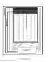
FIG. 1 is a schematic, structural view of a touch display panel of an in cell touch panel disclosed by the prior art.
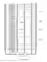
FIG. 2 is a schematic view of sensor pads in a full in-cell touch panel according to the prior art.
FIG. 3 is an equivalent circuit diagram of parasitic capacitance in the full in-cell touch panel according to the prior art.
FIG. 4 is a sequence diagram of inputting a first simulation signal, a second simulation signal and a third simulation signal in an elimination method of parasitic capacitance according to an embodiment of the disclosure.
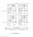
FIG. 5 is a schematic structural view of modules generating a first target high level, a second target high level, a first target low level and a second target low level according to the prior art.
FIG. 6 is a schematic structural view of modules generating a first target high level, a second target high level, a first target low level and a second target low level according to an embodiment of the disclosure.
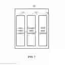
FIG. 7 is a schematic structural view of an elimination device of parasitic capacitance according to an embodiment of the disclosure.
DETAILED DESCRIPTION OF PREFERRED EMBODIMENTS
The disclosure firstly introduce a structure of an in cell touch panel and a scanning manner for convenience of comprehension. Referring to FIG. 1, FIG. 1 is a schematic, structural view of a touch display panel of an in cell touch panel disclosed by the prior art. The touch display panel shown in FIG. 1 includes a drive IC, a plurality of gate lines 1, a plurality of source electrode lines (not shown in the figure), a plurality of common electrode lines 2, a plurality of multiplex lines (not shown in the figure), an extension direction of the plurality of common electrode lines and an extension direction of the source electrode lines are parallel, as shown in FIG. 2, a common electrode on a side of a module is divided in a plurality of sensor pads 110, the plurality of common electrode lines 2 are connected to the plurality of sensor pads 110 respectively, the plurality of multiplex lines are connected to the plurality of gate lines 1 respectively.
The common electrode is generally multiplexed to be a touch driving electrode for reducing the entire thickness of the module. Therefore, a scanning cycle is at least divided in a display scanning period and a touch scanning period to achieve a display function and a touch function simultaneously. During the display scanning period, the drive IC inputs a display scanning signal to the plurality of gate lines 1 and inputs a VCOM voltage to the sensor pads 110, the display scanning is ran with coordination of the display scanning signal and the VCOM voltage. During the touch scanning period, the drive IC inputs a touch scanning signal to a plurality of touch sensing electrodes and inputs a pulsed voltage to the sensor pads 110, the touch scanning is ran with coordination of the touch scanning signal and the pulsed voltage.
However, as two adjacent pieces of metal can form a capacitor, an equivalent circuit diagram formed between two of the gate line, a first common electrode line, a second common electrode line and the source electrode line is shown as FIG. 3. One of the sensor pads 110 is taken as an example, capacitance between the first common electrode line and the second common electrode line can be equal to capacitance S1, capacitance between the first common electrode line and the gate line can be equal to S2, capacitance between the first common electrode line and the source electrode line can be equal to S3, capacitance between the second common electrode line and the source electrode line can be equal to S4, capacitance between the gate line and the source electrode line can be equal to S5. As existence of capacitance S1 to S5, during inputting a pulse-shaped touch scanning voltage to the sensor pad 110, voltages input to the gate line and the source electrode line are both direct voltages, which can cause a charging and discharging effect of capacitance to affect the input touch scanning signal during touch scanning and reduce a signal-to-noise ratio during touch scanning.
The embodiment of the disclosure provides an elimination method of parasitic capacitance to solve the problem above. The method includes during the touch scanning period inputting a first simulation signal to the plurality of source electrode lines, inputting a second simulation signal to the plurality of multiplex lines and inputting a third simulation signal to the plurality of gate lines for eliminating parasitic capacitance formed between two of the plurality of gate lines, the plurality of source electrode lines, the plurality of common electrode lines and the plurality of sensor pads. A waveform of the first simulation signal and a waveform of a touch scanning signal input in the common electrode are similar, a waveform of the second simulation signal and the waveform of the touch scanning signal input in the common electrode are similar, a waveform of the third simulation signal and the waveform of the touch scanning signal input in the common electrode are similar.
The first simulation signal, the second simulation signal and the third simulation signal being all similar to the touch scanning signal input to the common electrode indicates when the pulse-shaped touch scanning signal is a high level, the first simulation signal, the second simulation signal and the third simulation signal will also be the high level, when the pulse-shaped touch scanning signal is a low level, the first simulation signal, the second simulation signal and the third simulation signal will also be the low level. It can be comprehensible that when the first simulation signal, the second simulation signal, the third simulation signal and the touch scanning signal are the high levels (or low levels), voltage differences between two of the gate line, the first common electrode line, the second common electrode line and the source electrode line will be decreased to reduce the charging and discharging effects of the parasitic capacitance S1 to S5 between two of the gate line, the first common electrode line, the second common electrode line and the source electrode line.
In a practical embodiment, during the touch scanning period, an initial direct voltage on the plurality of source electrode lines is zero, therefore, the drive IC inputs the first simulation signal with a voltage identical to the touch scanning signal to the source electrode lines. An initial voltage on the plurality of multiplex lines is VGH, therefore, the second simulation signal inputting from the drive IC to the multiplex lines includes a first target high level and a second target high level, where the first target high level is higher than the second target high level, moreover, a value of the first target high level and that of the second target high level have no significant difference compared with a value of the VGH voltage. An initial voltage on the gate lines is VGL, therefore, the third simulation signal inputting from the drive IC to the gate lines includes a first target low level and a second target low level, where the first target low level is higher than the second target low level, moreover, a value of the first target low level and that of the second target low level have no significant difference compared with a value of the VGL voltage. In some circumstances, the second target high level can be higher than the first target low level.
As shown in FIG. 5, in a conventional technique, a module merely has one VGH module and one VGL module, however, the conventional VGH module and VGL module both have a multiplex output function. Various voltages can be output via various paths by selecting various modes. Therefore, the VGH module can generate the first target high level and the second target high level, the VGL module can generate the first target low level and the second target low level.
However, conversion efficiency of the voltage is low according to the manner above, therefore, in order to boost voltage conversion efficiency, the first target high level and the second target high level can be generated by various VGH modules, the first target low level and the second target low level can be generated by various VGL modules. For instance, as shown in FIG. 6, the module is disposed with two VGH modules containing a first VGH module and a second VGH module, also disposed with two VGL modules containing a first VGL module and a second VGL module. The first target high level is generated by the first VGH module, the second target high level is generated by the second VGH module, the first target low level is generated by the first VGL module, the second target low level is generated by the second VGL module. Generating the first target high level and the second target high level by various VGH modules and generating the first target low level and the second target low level by various VGL modules can improve efficiency of converting voltages efficiently.
The embodiment of the disclosure has been described in detail above, a device will be provided as follows to better implement the embodiment of the disclosure above correspondingly.
Referring to FIG. 7, FIG. 7 provides an elimination device of parasitic capacitance. A device 70 of the embodiment includes a plurality of gate lines, a plurality of source electrode lines, a plurality of common electrode lines, a plurality of multiplex lines, an extension direction of the plurality of common electrode lines and an extension direction of the source electrode lines are parallel. A common electrode includes a plurality of sensor pads, the common electrode is multiplexed to be a touch driving electrode, the plurality of common electrode lines are connected to the plurality of sensor pads respectively. The plurality of multiplex lines are connected to the plurality of gate lines respectively. A scanning cycle includes a display scanning period and a touch scanning period. The device 70 includes a first input module 71, a second input module 72 and a third input module 73.
The first input module 71 is configured to input the first simulation signal to the plurality of source electrode lines during the touch scanning period. The second input module 72 is configured to input the second simulation signal to the plurality of multiplex lines. The third input module 73 is configured to input the third simulation signal to the plurality of gate lines. Which eliminate parasitic capacitance formed between two of the plurality of gate lines, the plurality of source electrode lines, the plurality of common electrode lines and the plurality of sensor pads. A waveform of the first simulation signal and a waveform of a scanning signal input in the common electrode are similar, a waveform of the second simulation signal and the waveform of the scanning signal input in the common electrode are similar, a waveform of the third simulation signal and the waveform of the scanning signal input in the common electrode are similar.
Optionally, the waveform of the second simulation signal includes a first target high level and a second target high level. The waveform of the second simulation signal includes a first target low level and a second target low level. The first target high level and the second target high level are generated by different VGH modules, the first target low level and the second target low level are generated by different VGL modules.
Optionally, the first target high level is generated by a first VGH module, the second target high level is generated by a second VGH module, the first target low level is generated by a first VGL module, the second target low level is generated by a second VGL module.
Optionally, the first target high level>the second target high level>the first target low level>the second target low level.
Optionally, the waveform of the first simulation signal and the waveform of the scanning signal input in the common electrode are identical.
In embodiments of the disclosure, inputting the first simulation signal with a waveform similar to the touch scanning signal input in the common electrode to the plurality of source electrode lines, inputting the second simulation signal with a waveform similar to the touch scanning signal input in the common electrode to the plurality of multiplex lines and inputting the third simulation signal with a waveform similar to the touch scanning signal input in the common electrode to the plurality of gate lines can reduce influence of parasitic capacitance in a full in-cell touch panel on the input touch scanning signal.
It is understandable in practical to a person skilled in the art that all or portion of the processes in the method according to the aforesaid embodiment can be accomplished with the computer program to instruct the related hardware. The program can be stored in a readable storage medium of a computer. When the program is executed, the processes of the embodiments in the aforesaid respective methods can be included. The storage medium can be a disk, a compact disc, a Read-Only Memory (ROM) or a Random Access Memory (RAM).
Above are merely preferred embodiments of the disclosure, which do not limit the protection scope of the disclosure. A person skilled in the art can understand and achieve all or portion of the processes of the aforesaid embodiments to obtain equivalent replacements that should be covered by the protected scope of the disclosure as well.
Claims
What is claimed is:1. An elimination method of parasitic capacitance, wherein the touch display panel comprises a plurality of gate lines, a plurality of source electrode lines, a plurality of common electrode lines, a plurality of multiplex lines, an extension direction of the plurality of common electrode lines and an extension direction of the source electrode lines are parallel, a common electrode comprises a plurality of sensor pads, the common electrode is multiplexed to be a touch driving electrode, the plurality of common electrode lines are connected to the plurality of sensor pads respectively, the plurality of multiplex lines are connected to the plurality of gate lines respectively, a scanning cycle comprises a display scanning period and a touch scanning period,
during the touch scanning period, inputting a first simulation signal to the plurality of source electrode lines, inputting a second simulation signal to the plurality of multiplex lines and inputting a third simulation signal to the plurality of gate lines for eliminating parasitic capacitance formed among the plurality of gate lines, the plurality of source electrode lines, the plurality of common electrode lines and the plurality of sensor pads;
wherein a waveform of the first simulation signal and a waveform of a scanning signal input in the common electrode are similar, a waveform of the second simulation signal and the waveform of the scanning signal input in the common electrode are similar, a waveform of the third simulation signal and the waveform of the scanning signal input in the common electrode are similar.
2. The method according to claim 1, wherein the waveform of the second simulation signal comprises a first target high level and a second target high level, the waveform of the second simulation signal comprises a first target low level and a second target low level, the first target high level and the second target high level are generated by different VGH modules, the first target low level and the second target low level are generated by different VGL modules.
3. The method according to claim 2, wherein the first target high level is generated by a first VGH module, the second target high level is generated by a second VGH module, the first target low level is generated by a first VGL module, the second target low level is generated by a second VGL module.
4. The method according to claim 2, wherein the first target high level>the second target high level>the first target low level>the second target low level.
5. The method according to claim 1, wherein the waveform of the first simulation signal and the waveform of the scanning signal input in the common electrode are identical.
6. An elimination device of parasitic capacitance, wherein the touch display panel comprises a plurality of gate lines, a plurality of source electrode lines, a plurality of common electrode lines, a plurality of multiplex lines, an extension direction of the plurality of common electrode lines and an extension direction of the source electrode lines are parallel, a common electrode comprises a plurality of sensor pads, the common electrode is multiplexed to be a touch driving electrode, the plurality of common electrode lines are connected to the plurality of sensor pads respectively, the plurality of multiplex lines are connected to the plurality of gate lines respectively, a scanning cycle comprises a display scanning period and a touch scanning period, the device comprises a first input module, a second input module and a third input module,
the first input module being configured to input a first simulation signal to the plurality of source electrode lines during the touch scanning period, the second input module being configured to input a second simulation signal to the plurality of multiplex lines, the third input module being configured to input a third simulation signal to the plurality of gate lines, so as to eliminate parasitic capacitance formed among the plurality of gate lines, the plurality of source electrode lines, the plurality of common electrode lines and the plurality of sensor pads;
wherein a waveform of the first simulation signal and a waveform of a scanning signal input in the common electrode are similar, a waveform of the second simulation signal and the waveform of the scanning signal input in the common electrode are similar, a waveform of the third simulation signal and the waveform of the scanning signal input in the common electrode are similar.
7. The device according to claim 6, wherein the waveform of the second simulation signal comprises a first target high level and a second target high level, the waveform of the second simulation signal comprises a first target low level and a second target low level, the first target high level and the second target high level are generated by different VGH modules, the first target low level and the second target low level are generated by different VGL modules.
8. The device according to claim 7, wherein the first target high level is generated by a first VGH module, the second target high level is generated by a second VGH module, the first target low level is generated by a first VGL module, the second target low level is generated by a second VGL module.
9. The device according to claim 8, wherein the first target high level>the second target high level>the first target low level>the second target low level.
10. The device according to claim 7, wherein the waveform of the first simulation signal and the waveform of the scanning signal input in the common electrode are identical.
Images & Drawings included:

Sources:
- United States Patent and Trademark Office - verify current appl. status at the USPTO↗
Recent applications in this class:
- » 20250284359 2025-09-11
DISPLAY DEVICE - » 20250271959 2025-08-28
LIGHTING TOUCHPAD - » 20250271958 2025-08-28
DISPLAY DEVICE - » 20250264954 2025-08-21
WEARABLE DEVICE AND METHOD FOR IDENTIFYING TOUCH INPUT, AND NON-TRANSITORY COMPUTER-READABLE STORAGE MEDIUM - » 20250264953 2025-08-21
STATIC ELECTRICITY PREVENTION METHOD, AND ELECTRONIC DEVICE THEREFOR - » 20250264952 2025-08-21
Touch Display Device - » 20250258560 2025-08-14
INDICATED POSITION DETECTING DEVICE AND INDICATED POSITION DETECTING METHOD - » 20250258559 2025-08-14
Electronic Device - » 20250251816 2025-08-07
ELECTRONIC DEVICE WITH GLASS ENCLOSURE - » 20250251815 2025-08-07
ELECTRONIC DEVICE
Recent applications for this Assignee:
- » 20250252896 2025-08-07
PIXEL DRIVING CIRCUIT AND DISPLAY PANEL - » 20250248193 2025-07-31
DISPALY PANEL AND DISPLAY MODULE - » 20250244850 2025-07-31
TOUCH DISPLAY DEVICES AND TOUCH METHODS THEREOF - » 20250244577 2025-07-31
DISPLAY MODULE AND FIELD-OF-VIEW DISPLAY DEVICE FOR VEHICLE - » 20250225913 2025-07-10
LIGHT BOARDS AND DISPLAY PANELS - » 20250221126 2025-07-03
DISPLAY BACKPLANE AND DISPLAY DEVICE - » 20250212512 2025-06-26
DISPLAY PANEL - » 20250210003 2025-06-26
DISPLAY DEVICE AND ELECTRONIC DEVICE - » 20250182713 2025-06-05
GOA CIRCUIT AND DISPLAY PANEL - » 20250159934 2025-05-15
TRANSISTOR STRUCTURES, DRIVING SUBSTRATES AND DISPLAY PANELS