Organic electroluminescent device and manufacturing method thereof
US20180175294A1
2018-06-21
15/737,179
2016-06-15
✅ Patent granted
US 11,437,582 B2
2022-09-06
WO; PCT/CN2016/085802; 20160615
WO; WO2016/202251; 20161222
Andrew K Bohaty
Kilpatrick Townsend & Stockton
2038-02-07
Abstract:
Disclosed is an organic electroluminescent device, comprising a substrate and light emitting units formed in sequence on the substrate, characterized in that, each of the light emitting units comprises a first electrode layer (1), a light emitting layer (2) and a second electrode layer (3), the light emitting layer comprises a host material and a dye, the host material is made of materials having both electron transport capability and hole transport capability; at least one material in the host material has a CT excited triplet state energy level T1 greater than its n-π excited triplet state energy level S1, and T1-S1≤0.3 eV; or, at least one material in the host material has a CT excited triplet state energy level T1 greater than its n-π excited triplet state energy level S1, and T1-S1≥1 eV, with the difference between its n-π excited second triplet state energy level and its CT excited first singlet state energy level being in the range of −0.1 eV to 0.1 eV. The organic electroluminescent device configuration can sufficiently utilize the triplet state energy in the host material and the dye to increase the luminous efficiency and prolong the service life of the device.
Inventors:
- Song LIU 72 🇨🇳 Beijing, China
- Lian DUAN 24 🇨🇳 Beijing, China
- Dongdong ZHANG 55 🇨🇳 Beijing, China
- Fei ZHAO 24 🇨🇳 Beijing, China
- Jing Xie 3 🇨🇳 Hebei, China
Assignee:
- Tsinghua University 3,118 🇨🇳 Beijing, China
- KUNSHAN GO-VISIONOX OPTO-ELECTRONICS CO., LTD. 460 🇨🇳 KunShan, China
Applicant:
Interested in similar patents?
Get notified when new applications in this technology area are published.
Classification:
C07C2603/97 » CPC further
Systems containing at least three condensed rings; Spiro compounds containing "not free" spiro atoms containing at least one ring with less than six members containing five-membered rings
C07C255/58 » CPC further
Carboxylic acid nitriles having cyano groups bound to carbon atoms of six-membered aromatic rings of a carbon skeleton containing cyano groups and singly-bound nitrogen atoms, not being further bound to other hetero atoms, bound to the carbon skeleton
C07D285/14 » CPC further
Heterocyclic compounds containing rings having nitrogen and sulfur atoms as the only ring hetero atoms, not provided for by groups - ; Five-membered rings; Thiadiazoles; Hydrogenated thiadiazoles condensed with carbocyclic rings or ring systems
H01L51/006 » CPC main
Solid state devices using organic materials as the active part, or using a combination of organic materials with other materials as the active part; Processes or apparatus specially adapted for the manufacture or treatment of such devices, or of parts thereof; Selection of organic semiconducting materials, e.g. organic light sensitive or organic light emitting materials; Macromolecular systems with low molecular weight, e.g. cyanine dyes, coumarine dyes, tetrathiafulvalene; Amine compounds having at least two aryl rest on at least one amine-nitrogen atom, e.g. triphenylamine comprising polycyclic condensed aromatic hydrocarbons as substituents on the nitrogen atom
C07D417/04 » CPC further
Heterocyclic compounds containing two or more hetero rings, at least one ring having nitrogen and sulfur atoms as the only ring hetero atoms, not provided for by group containing two hetero rings directly linked by a ring-member-to-ring-member bond
C07D417/10 » CPC further
Heterocyclic compounds containing two or more hetero rings, at least one ring having nitrogen and sulfur atoms as the only ring hetero atoms, not provided for by group containing two hetero rings linked by a carbon chain containing aromatic rings
C07D417/14 » CPC further
Heterocyclic compounds containing two or more hetero rings, at least one ring having nitrogen and sulfur atoms as the only ring hetero atoms, not provided for by group containing three or more hetero rings
C07D471/20 » CPC further
Heterocyclic compounds containing nitrogen atoms as the only ring hetero atoms in the condensed system, at least one ring being a six-membered ring with one nitrogen atom, not provided for by groups - in which the condensed system contains three hetero rings Spiro-condensed systems
C07D487/14 » CPC further
Heterocyclic compounds containing nitrogen atoms as the only ring hetero atoms in the condensed system, not provided for by groups - in which the condensed system contains three hetero rings Ortho-condensed systems
C07D487/16 » CPC further
Heterocyclic compounds containing nitrogen atoms as the only ring hetero atoms in the condensed system, not provided for by groups - in which the condensed system contains three hetero rings Peri-condensed systems
C07F1/02 » CPC further
Compounds containing elements of Groups 1 or 11 of the Periodic System Lithium compounds
C07F3/02 » CPC further
Compounds containing elements of Groups 2 or 12 of the Periodic System Magnesium compounds
C07F3/06 » CPC further
Compounds containing elements of Groups 2 or 12 of the Periodic System Zinc compounds
H01L51/007 » CPC further
Solid state devices using organic materials as the active part, or using a combination of organic materials with other materials as the active part; Processes or apparatus specially adapted for the manufacture or treatment of such devices, or of parts thereof; Selection of organic semiconducting materials, e.g. organic light sensitive or organic light emitting materials; Macromolecular systems with low molecular weight, e.g. cyanine dyes, coumarine dyes, tetrathiafulvalene aromatic compounds comprising a hetero atom, e.g.: N,P,S comprising two or more different heteroatoms per ring, e.g. S and N Oxadiazole compounds
C07C317/36 » CPC further
Sulfones; Sulfoxides having sulfone or sulfoxide groups and nitrogen atoms, not being part of nitro or nitroso groups, bound to the same carbon skeleton with sulfone or sulfoxide groups bound to carbon atoms of six-membered aromatic rings of the carbon skeleton having sulfone or sulfoxide groups and amino groups bound to carbon atoms of six-membered aromatic rings being part of the same non-condensed ring or of a condensed ring system containing that ring with the nitrogen atoms of the amino groups bound to hydrogen atoms or to carbon atoms
C07D209/80 » CPC further
Heterocyclic compounds containing five-membered rings, condensed with other rings, with one nitrogen atom as the only ring hetero atom; Ring systems containing three or more rings [b, c]- or [b, d]-condensed
C07D209/86 » CPC further
Heterocyclic compounds containing five-membered rings, condensed with other rings, with one nitrogen atom as the only ring hetero atom; Ring systems containing three or more rings [b, c]- or [b, d]-condensed; Carbazoles; Hydrogenated carbazoles with only hydrogen atoms, hydrocarbon or substituted hydrocarbon radicals, directly attached to carbon atoms of the ring system
C07D219/02 » CPC further
Heterocyclic compounds containing acridine or hydrogenated acridine ring systems with only hydrogen, hydrocarbon or substituted hydrocarbon radicals, directly attached to carbon atoms of the ring system
C07D221/20 » CPC further
Heterocyclic compounds containing six-membered rings having one nitrogen atom as the only ring hetero atom, not provided for by groups - condensed with carbocyclic rings or ring systems Spiro-condensed ring systems
C07D241/48 » CPC further
Heterocyclic compounds containing 1,4-diazine or hydrogenated 1,4-diazine rings condensed with carbocyclic rings or ring systems with only hydrogen or carbon atoms directly attached to the ring nitrogen atoms; Phenazines with hydrocarbon radicals, substituted by nitrogen atoms, directly attached to the ring nitrogen atoms
C07D265/38 » CPC further
Heterocyclic compounds containing six-membered rings having one nitrogen atom and one oxygen atom as the only ring hetero atoms 1,4-Oxazines; Hydrogenated 1,4-oxazines condensed with carbocyclic rings [b, e]-condensed with two six-membered rings
C07D403/10 » CPC further
Heterocyclic compounds containing two or more hetero rings, having nitrogen atoms as the only ring hetero atoms, not provided for by group containing two hetero rings linked by a carbon chain containing aromatic rings
C07D403/14 » CPC further
Heterocyclic compounds containing two or more hetero rings, having nitrogen atoms as the only ring hetero atoms, not provided for by group containing three or more hetero rings
C07D413/10 » CPC further
Heterocyclic compounds containing two or more hetero rings, at least one ring having nitrogen and oxygen atoms as the only ring hetero atoms containing two hetero rings linked by a carbon chain containing aromatic rings
C07D413/14 » CPC further
Heterocyclic compounds containing two or more hetero rings, at least one ring having nitrogen and oxygen atoms as the only ring hetero atoms containing three or more hetero rings
H01L51/0059 » CPC further
Solid state devices using organic materials as the active part, or using a combination of organic materials with other materials as the active part; Processes or apparatus specially adapted for the manufacture or treatment of such devices, or of parts thereof; Selection of organic semiconducting materials, e.g. organic light sensitive or organic light emitting materials; Macromolecular systems with low molecular weight, e.g. cyanine dyes, coumarine dyes, tetrathiafulvalene Amine compounds having at least two aryl rest on at least one amine-nitrogen atom, e.g. triphenylamine
H01L51/0061 » CPC further
Solid state devices using organic materials as the active part, or using a combination of organic materials with other materials as the active part; Processes or apparatus specially adapted for the manufacture or treatment of such devices, or of parts thereof; Selection of organic semiconducting materials, e.g. organic light sensitive or organic light emitting materials; Macromolecular systems with low molecular weight, e.g. cyanine dyes, coumarine dyes, tetrathiafulvalene; Amine compounds having at least two aryl rest on at least one amine-nitrogen atom, e.g. triphenylamine comprising heteroaromatic hydrocarbons as substituents on the nitrogen atom
H01L51/0067 » CPC further
Solid state devices using organic materials as the active part, or using a combination of organic materials with other materials as the active part; Processes or apparatus specially adapted for the manufacture or treatment of such devices, or of parts thereof; Selection of organic semiconducting materials, e.g. organic light sensitive or organic light emitting materials; Macromolecular systems with low molecular weight, e.g. cyanine dyes, coumarine dyes, tetrathiafulvalene aromatic compounds comprising a hetero atom, e.g.: N,P,S comprising only nitrogen as heteroatom
H01L51/0068 » CPC further
Solid state devices using organic materials as the active part, or using a combination of organic materials with other materials as the active part; Processes or apparatus specially adapted for the manufacture or treatment of such devices, or of parts thereof; Selection of organic semiconducting materials, e.g. organic light sensitive or organic light emitting materials; Macromolecular systems with low molecular weight, e.g. cyanine dyes, coumarine dyes, tetrathiafulvalene aromatic compounds comprising a hetero atom, e.g.: N,P,S comprising only sulfur as heteroatom
H01L51/0069 » CPC further
Solid state devices using organic materials as the active part, or using a combination of organic materials with other materials as the active part; Processes or apparatus specially adapted for the manufacture or treatment of such devices, or of parts thereof; Selection of organic semiconducting materials, e.g. organic light sensitive or organic light emitting materials; Macromolecular systems with low molecular weight, e.g. cyanine dyes, coumarine dyes, tetrathiafulvalene aromatic compounds comprising a hetero atom, e.g.: N,P,S comprising two or more different heteroatoms per ring, e.g. S and N
H01L51/0071 » CPC further
Solid state devices using organic materials as the active part, or using a combination of organic materials with other materials as the active part; Processes or apparatus specially adapted for the manufacture or treatment of such devices, or of parts thereof; Selection of organic semiconducting materials, e.g. organic light sensitive or organic light emitting materials; Macromolecular systems with low molecular weight, e.g. cyanine dyes, coumarine dyes, tetrathiafulvalene aromatic compounds comprising a hetero atom, e.g.: N,P,S Polycyclic condensed heteroaromatic hydrocarbons
H01L51/0072 » CPC further
Solid state devices using organic materials as the active part, or using a combination of organic materials with other materials as the active part; Processes or apparatus specially adapted for the manufacture or treatment of such devices, or of parts thereof; Selection of organic semiconducting materials, e.g. organic light sensitive or organic light emitting materials; Macromolecular systems with low molecular weight, e.g. cyanine dyes, coumarine dyes, tetrathiafulvalene aromatic compounds comprising a hetero atom, e.g.: N,P,S; Polycyclic condensed heteroaromatic hydrocarbons comprising only nitrogen in the heteroaromatic polycondensed ringsystem, e.g. phenanthroline, carbazole
H01L51/0077 » CPC further
Solid state devices using organic materials as the active part, or using a combination of organic materials with other materials as the active part; Processes or apparatus specially adapted for the manufacture or treatment of such devices, or of parts thereof; Selection of organic semiconducting materials, e.g. organic light sensitive or organic light emitting materials Coordination compounds, e.g. porphyrin
H01L51/0092 » CPC further
Solid state devices using organic materials as the active part, or using a combination of organic materials with other materials as the active part; Processes or apparatus specially adapted for the manufacture or treatment of such devices, or of parts thereof; Selection of organic semiconducting materials, e.g. organic light sensitive or organic light emitting materials; Coordination compounds, e.g. porphyrin Metal complexes comprising a IIB-metal (Zn, Cd, Hg)
H01L51/5012 » CPC further
Solid state devices using organic materials as the active part, or using a combination of organic materials with other materials as the active part; Processes or apparatus specially adapted for the manufacture or treatment of such devices, or of parts thereof specially adapted for light emission, e.g. organic light emitting diodes [OLED] or polymer light emitting devices [PLED] Electroluminescent [EL] layer
C07C2603/24 » CPC further
Systems containing at least three condensed rings; Ortho- or ortho- and peri-condensed systems containing three rings containing only six-membered rings Anthracenes; Hydrogenated anthracenes
H01L51/0008 » CPC further
Solid state devices using organic materials as the active part, or using a combination of organic materials with other materials as the active part; Processes or apparatus specially adapted for the manufacture or treatment of such devices, or of parts thereof; Processes specially adapted for the manufacture or treatment of devices or of parts thereof; Deposition of organic semiconductor materials on a substrate using physical deposition, e.g. sublimation, sputtering
H01L51/0052 » CPC further
Solid state devices using organic materials as the active part, or using a combination of organic materials with other materials as the active part; Processes or apparatus specially adapted for the manufacture or treatment of such devices, or of parts thereof; Selection of organic semiconducting materials, e.g. organic light sensitive or organic light emitting materials; Macromolecular systems with low molecular weight, e.g. cyanine dyes, coumarine dyes, tetrathiafulvalene Polycyclic condensed aromatic hydrocarbons, e.g. anthracene
H01L51/0056 » CPC further
Solid state devices using organic materials as the active part, or using a combination of organic materials with other materials as the active part; Processes or apparatus specially adapted for the manufacture or treatment of such devices, or of parts thereof; Selection of organic semiconducting materials, e.g. organic light sensitive or organic light emitting materials; Macromolecular systems with low molecular weight, e.g. cyanine dyes, coumarine dyes, tetrathiafulvalene; Polycyclic condensed aromatic hydrocarbons, e.g. anthracene containing six or more rings
H01L51/5016 » CPC further
Solid state devices using organic materials as the active part, or using a combination of organic materials with other materials as the active part; Processes or apparatus specially adapted for the manufacture or treatment of such devices, or of parts thereof specially adapted for light emission, e.g. organic light emitting diodes [OLED] or polymer light emitting devices [PLED]; Electroluminescent [EL] layer Triplet emission
H01L51/5024 » CPC further
Solid state devices using organic materials as the active part, or using a combination of organic materials with other materials as the active part; Processes or apparatus specially adapted for the manufacture or treatment of such devices, or of parts thereof specially adapted for light emission, e.g. organic light emitting diodes [OLED] or polymer light emitting devices [PLED]; Electroluminescent [EL] layer having a host comprising an emissive dopant and further additive materials, e.g. for improving the dispersability, for improving the stabilisation, for assisting energy transfer
H01L51/5056 » CPC further
Solid state devices using organic materials as the active part, or using a combination of organic materials with other materials as the active part; Processes or apparatus specially adapted for the manufacture or treatment of such devices, or of parts thereof specially adapted for light emission, e.g. organic light emitting diodes [OLED] or polymer light emitting devices [PLED]; Carrier transporting layer Hole transporting layer
H01L51/5072 » CPC further
Solid state devices using organic materials as the active part, or using a combination of organic materials with other materials as the active part; Processes or apparatus specially adapted for the manufacture or treatment of such devices, or of parts thereof specially adapted for light emission, e.g. organic light emitting diodes [OLED] or polymer light emitting devices [PLED]; Carrier transporting layer Electron transporting layer
H01L2251/5376 » CPC further
Indexing scheme relating to organic semiconductor devices covered by group; Organic light emitting devices; Structure Combination of fluorescent and phosphorescent emission
H01L2251/5384 » CPC further
Indexing scheme relating to organic semiconductor devices covered by group; Organic light emitting devices; Structure Multiple hosts in the emissive layer
H01L2251/558 » CPC further
Indexing scheme relating to organic semiconductor devices covered by group; Organic light emitting devices characterised by parameters Thickness
H01L51/00 IPC
Solid state devices using organic materials as the active part, or using a combination of organic materials with other materials as the active part; Processes or apparatus specially adapted for the manufacture or treatment of such devices, or of parts thereof
H01L51/50 IPC
Solid state devices using organic materials as the active part, or using a combination of organic materials with other materials as the active part; Processes or apparatus specially adapted for the manufacture or treatment of such devices, or of parts thereof specially adapted for light emission, e.g. organic light emitting diodes [OLED] or polymer light emitting devices [PLED]
C07C211/61 » CPC further
Compounds containing amino groups bound to a carbon skeleton having amino groups bound to carbon atoms of six-membered aromatic rings of the carbon skeleton having amino groups bound to carbon atoms of six-membered aromatic rings being part of condensed ring systems of the carbon skeleton with at least one of the condensed ring systems formed by three or more rings
Description
TECHNICAL FIELD
The present invention relates to the technical field of organic electroluminescent devices, and in particular relates to an organic electroluminescent device with a single-layered organic layer.
BACKGROUND
An organic electroluminescent device (OLED) usually includes a plurality of pixels, and each pixel is composed of several sub-pixels. Currently, one widely used solution in small and medium sized devices is forming a pixel with three sub-pixels of red, green and blue. Each kind of sub-pixel comprises a hole transport layer, a light emitting layer, an electron transport layer, and a hole/exciton blocking layer arranged between the light emitting layer and the electron transport layer, wherein the light emitting layer comprises a blue light emitting layer, a green light emitting layer or a red light emitting layer. Besides, a green optical compensation layer and a red light emitting layer might be required to be arranged between the hole transport layer and an electrode layer, which further adds to the processing steps.
In order to solve the above-mentioned problem, it is explored to use a device configuration with a single-layered light emitting layer. However, in conventional OLED devices with single-layered light emitting layer, because most organic materials have imbalanced carrier injection and different carriers have hugely different transporting speed, the light emitting area easily shifts to the side of the injection electrode with a lower migration rate. In the condition of a metal electrode, this may easily cause light-emitting to be quenched by the electrode, which negatively affects the efficiency and service life of the device.
SUMMARY OF THE INVENTION
Thus, the present invention is intended to solve the technical problem that the organic electroluminescent devices in prior arts with the existing configuration of single-layered structure have a short service life because of exciton quenching, by providing an organic electroluminescent device that can sufficiently utilize the triplet state energy in the host material and the dye to increase the luminous efficiency and prolong the service life of the device.
The present invention also provides a preparation method of the above-mentioned organic electroluminescent device.
In order to solve the above-mentioned technical problem, the present invention adopts the following technical scheme:
An organic electroluminescent device comprises a substrate and light emitting units formed in sequence on the substrate, and each of the light emitting units comprises a first electrode layer, a light emitting layer and a second electrode layer, the light emitting layer comprises a host material and a dye, the host material is made of materials having both electron transport capability and hole transport capability; at least one material in the host material has a CT excited triplet state energy level T1 greater than its n-π excited triplet state energy level S1, and T1-S1≤0.3 eV; or, at least one material in the host material has a CT excited triplet state energy level T1 greater than its n-π excited triplet state energy level S1, and T1-S1≥1 eV, with the difference between its n-π excited second triplet state energy level and its CT excited first singlet state energy level being in the range of −0.1 eV to 0.1 eV.
Preferably, the host material is an exciplex, and the exciplex is a thermal activating delayed fluorescence material.
Alternatively, the host material is an exciplex made from an electron transport type material and a hole transport type material at a mass ratio of 1:9 to 9:1. Wherein, the electron transport type material and/or the hole transport type material has T1-S1≤0.3 eV; or, the electron transport type material and/or the hole transport type material has T1-S1≥1 eV, with the difference between the n-π excited second triplet state energy level and the CT excited first singlet state energy level of the host material being in the range of −0.1 eV to 0.1 eV.
Alternatively, the host material is composed of a thermal activating delayed fluorescence material and a hole transport type material at a mass ratio of 1:9 to 9:1. Wherein, the thermal activating delayed fluorescence material and/or the hole transport type material has T1-S1≤0.3 eV; or, the thermal activating delayed fluorescence material and/or the hole transport type material has T1-S1≥1 eV, with the difference between the n-π excited second triplet state energy level and the CT excited first singlet state energy level of the host material being in the range of −0.1 eV to 0.1 eV.
Alternatively, the host material is composed of a thermal activating delayed fluorescence material and an electron transport type material at a mass ratio of 1:9 to 9:1. Wherein, the thermal activating delayed fluorescence material and/or the electron transport type material has T1-S1≤0.3 eV; or, the thermal activating delayed fluorescence material and/or the electron transport type material has T1-S1≥1 eV, with the difference between the n-π excited second triplet state energy level and the CT excited first singlet state energy level of the host material being in the range of −0.1 eV to 0.1 eV.
The dye is made of a fluorescence material and/or a phosphorescence material, the fluorescence material has a doping concentration of 0.5-10 wt %, the phosphorescence material has a doping concentration of 0.5-20 wt %.
The light emitting layer has a thickness of 50 nm-150 nm.
The electron transport type material is tri-(8-oxyquinoline)-aluminum, 2,9-dimethyl-4,7-diphenyl-1,10-o-phenanthroline, 4,7-diphenyl-1,10-o-phenanthroline, di-(2-methyl-8-quinolyl)-4-phenyl-phenoxide-aluminum(III), 1,3,5-tri-(1-phenyl-1H-benzimidazole-2-yl)-benzene, or 1,3,5-tri-[(3-pyridyl)-3-phenyl]-benzene.
The hole transport type material is N,N′-di-(1-naphthyl)-N,N′-diphenyl-1,1′-biphenyl-4,4′-diamine, N,N′-diphenyl-N,N′-di-(m-methyl-phenyl)-1,1′-biphenyl-4,4′-diamine, 4,4′-cyclohexyl-di-[N,N-di-(4-methyl-phenyl)]-phenylamine, 4,4′-N,N′-di-carbazole-biphenyl, 4,4′,4″-tri-(carbazole-9-yl)-triphenylamine, or 1,3-di-(carbazole-9-yl)-benzene.
The thermal activating delayed fluorescence (TADF) material has a structure selected from the following structural formulas (1-1) to (1-100):
A preparation method of the aforementioned organic electroluminescent device comprises the following steps:
-
- evaporation coating a first electrode layer, a light emitting layer and a second electrode layer in sequence on a substrate by using an open mask;
- wherein, the light emitting layer is prepared by co-evaporation coating of a host material and a dye.
As compared to prior arts, the above-mentioned technical scheme of the present invention has the following advantages:
(1) The present invention aims to providing a single-layered device configuration, wherein the organic electroluminescent device only needs to consist of a first electrode layer, a light emitting layer and a second electrode layer, and the light emitting layer is prepared by co-evaporation coating of only a host material and a dye, without the necessity to prepare other organic layers such as a hole transport layer, a hole blocking layer, an electron transport layer or an electron blocking layer, so that the structure of the device is greatly simplified, the preparation process is shortened, and the production cost is reduced.
(2) In the present invention, the host material has T1-S1≤0.3 eV, such material has small difference between its singlet state energy level and its triplet state energy level, in particular, the host material may be a thermal activating delayed fluorescence material (TADF), or an exciplex made from an electron transport type material and a hole transport type material, or a composition made from a thermal activating delayed fluorescence material (TADF) and a hole transport type material, or a composition made from a thermal activating delayed fluorescence material (TADF) and an electron transport type material, these three types of compositions have donor groups and receptor groups, and therefore have capabilities to transport both holes and electrons. Meanwhile, the device configuration adopted by the present invention can sufficiently utilize the triplet state energy in the host material and the dye, because the difference between the singlet state energy level and the triplet state energy level is small, which is beneficial for injection of electrons and holes, so that the problem of low efficiency and short service life caused by exciton quenching can be solved. Therefore, the luminous efficiency can be increased and the service life of the device can be prolonged.
BRIEF DESCRIPTION OF THE DRAWINGS
In order to make the content of the present invention more easy to be understood clearly, hereinafter, the present invention is further described in detail according to specific embodiments of the present invention with reference to the accompanying drawings, wherein,
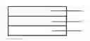
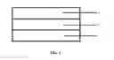
FIG. 1 is a structural schematic diagram of an organic electroluminescent device of the present invention.
Wherein: 1—first electrode layer, 2—light emitting layer, 3—second electrode layer.
DETAILED DESCRIPTION OF EMBODIMENTS
The present invention is further described hereinafter by illustrating specific embodiments.
The present invention can be implemented in many different forms, and should not be interpreted to be limited to the embodiments described herein. On the contrary, by providing these embodiments, the present disclosure is made complete and thorough, and the inventive concept of the present invention is sufficiently conveyed to those skilled in the art, wherein the present invention is defined by the Claims. In the accompanying drawings, for the sake of clarity, dimensions and relative sizes of layers and areas might be exaggerated. It should be understood that, when one element such as a layer, an area or a substrate plate is described as “formed on” or “configured on” another element, this one element may be configured directly upon that another element, or there may exist intermediate element(s). On the contrary, when one element is described as “directly formed upon” or “directly configured upon” another element, there exist no intermediate element.
As shown in FIG. 1, an organic electroluminescent device in the present invention comprises a substrate and light emitting units formed in sequence on the substrate, wherein, each of the light emitting units comprises a first electrode layer 1, a light emitting layer 2 and a second electrode layer 3; the light emitting layer comprises a host material and a dye; the host material is made of materials having both electron transport capability and hole transport capability; at least one material in the host material has a CT excited triplet state energy level T1 greater than its n-π excited triplet state energy level S1, and T1-S1≤0.3 eV; or, at least one material in the host material has a CT excited triplet state energy level T1 greater than its n-π excited triplet state energy level S1, and T1-S1≥1 eV, with the difference between its n-π excited second triplet state energy level and its CT excited first singlet state energy level being in the range of −0.1 eV to 0.1 eV.
A thermal activating delayed fluorescence material is a material in which there exists charge transfer transition. Both donor group units and receptor group units exist simultaneously in a thermal activating delayed fluorescence material, which gives the thermal activating delayed fluorescence material both electron transport capability and hole transport capability, wherein, the donor group unit is one donor group or a group formed by two or more donor groups being connected together, the receptor group unit is one receptor group or a group formed by two or more receptor groups being connected together. In particular, the thermal activating delayed fluorescence material has a structure selected from the structural formulas (1-1) to (1-100).
The host material in the present invention may be an exciplex made from a single thermal activating delayed fluorescence material, or an exciplex made from an electron transport type material and a hole transport type material, or a composition made from a thermal activating delayed fluorescence material (TADF) and a hole transport type material, or a composition made from a thermal activating delayed fluorescence material (TADF) and an electron transport type material.
The electron transport type material is tri-(8-oxyquinoline)-aluminum, 2,9-dimethyl-4,7-diphenyl-1,10-o-phenanthroline, 4,7-diphenyl-1,10-o-phenanthroline, di-(2-methyl-8-quinolyl)-4-phenyl-phenoxide-aluminum(III), 1,3,5-tri-(1-phenyl-1H-benzimidazole-2-yl)-benzene, or 1,3,5-tri-[(3-pyridyl)-3-phenyl]-benzene.
| Abbreviation | Full name | Structural formula |
| A1q3 | tri-(8-oxyquinoline)-aluminum | |
| BCP | 2,9-dimethyl-4,7-diphenyl-1,10- o-phenanthroline | |
| Bphen | 4,7-diphenyl-1,10-o-phenanthroline | |
| BAlq | di-(2-methyl-8-quinolyl)-4-phenyl- phenoxide-aluminum(III) | |
| TPBi | 1,3,5-tri-(1-phenyl-1H-benzimidazole-2-yl)- benzene | |
| TmPyPB | 1,3,5-tri-[(3-pyridyl)-3-phenyl]-benzene | |
The hole transport type material is N,N′-di-(1-naphthyl)-N,N′-diphenyl-1,1′-biphenyl-4,4′-diamine, N,N′-diphenyl-N,N′-di-(m-methyl-phenyl)-1,1′-biphenyl-4,4′-diamine, 4,4′-cyclohexyl-di-[N,N-di-(4-methyl-phenyl)]-phenylamine, 4,4′-N,N′-di-carbazole-biphenyl, 4,4′,4″-tri-(carbazole-9-yl)-triphenylamine, or 1,3-di-(carbazole-9-yl)-benzene.
| Abbreviation | Full name | Structural formula |
| NPB | N,N′-di-(1-naphthyl)-N,N′-diphenyl- 1,1′-biphenyl-4,4′-diamine | |
| TPD | N,N′-diphenyl- N,N′-di-(m-methyl-phenyl)- 1,1′-biphenyl-4,4′-diamine | |
| TAPC | 4,4′-cyclohexyl- di-[N,N-di-(4-methyl-phenyl)]- phenylamine | |
| CBP | 4,4′-N,N′-di-carbazole-biphenyl | |
| TCTA | 4,4′,4″-tri-(carbazole-9-yl)- triphenylamine | |
| mCP | 1,3-di-(carbazole-9-yl)-benzene | |
The red dye used in the present invention is selected from the following structural formulas:
The green dye used in the present invention is selected from the following structural formulas:
The blue dye used in the present invention is selected from the following structural formulas:
Embodiment 1
A device 1 of this embodiment has the following structure:
glass/ITO/(1-24):CBP:Ir(piq)2(acac)(5%)/cathode
The device 1 consists of a substrate, an anode layer, a light emitting layer and a cathode layer, without any hole injection layer, hole transport layer, electron injection layer or electron transport layer. The host material of the light emitting layer is made from the thermal activating delayed fluorescence material of the formula (1-24) and the hole transport type material of CBP, at a mass ratio of 1:1.
The preparation method of the device 1 is as follows: evaporation coating an anode layer (ITO), a light emitting layer and a cathode layer (cathode) in sequence on a substrate by using an open mask, wherein the light emitting layer is prepared by co-evaporation coating of a host material (1-24):CBP and a dye Ir(piq)2(acac), the doping concentration of the dye Ir(piq)2(acac) is 5 wt %.
Embodiment 2
A device 2 of this embodiment has the following structure:
glass/ITO/(1-88):BAlq:Ir(piq)2(acac)(5%)/cathode
In the device 2, the host material of the light emitting layer is made from an electron transport type material and the thermal activating delayed fluorescence material of the formula (1-88), at a mass ratio of 1:1. Herein, the thermal activating delayed fluorescence material serves as a hole transport type material.
The preparation method of the device 2 comprises the steps of evaporation coating an anode layer (ITO), a light emitting layer and a cathode layer (cathode) in sequence on a substrate by using an open mask, wherein the light emitting layer is prepared by co-evaporation coating of a host material (1-88):BAlq and a dye Ir(piq)2(acac), the doping concentration of the dye Ir(piq)2(acac) is 5 wt %.
Embodiment 3
A device 3 of this embodiment has the following structure:
glass/ITO/(1-88):(1-24):Ir(piq)2(acac)(5%)/cathode
In the device 3, the host material of the light emitting layer is an exciplex made from an electron transport type thermal activating delayed fluorescence material and a hole transport type thermal activating delayed fluorescence material), at a mass ratio of 1:1.
The preparation method of the device 3 is as follows: evaporation coating an anode layer (ITO), a light emitting layer and a cathode layer (cathode) in sequence on a substrate by using an open mask, wherein the light emitting layer is prepared by co-evaporation coating of a host material (1-88):(1-24) and a dye Ir(piq)2(acac), the doping concentration of the dye Ir(piq)2(acac) is 5 wt %.
COMPARISON EXAMPLE 1
A comparison device 1 of this example has the following structure:
glass/ITO/HIL/HTL/CBP:Ir(piq)2(acac)(5%)/HBL/ETL/cathode
COMPARISON EXAMPLE 2
A comparison device 2 of this example has the following structure:
glass/ITO/HIL/HTL/BAlq:Ir(piq)2(acac)(20%)/HBL/ETL/cathode
COMPARISON EXAMPLE 3
A comparison device 3 of this example has the following structure:
glass/ITO/HIL/HTL/CBP:BAlq:Ir(piq)2(acac)(5%)/HBL/ETL/cathode
| TABLE 1 | ||||
| Luminous | External | |||
| Brightness | efficiency | quantum | Service life T90 | |
| Device | (cd/m2) | (cd/A) | efficiency (%) | (hrs) |
| Device 1 | 5000 | 22 | 24 | 500 |
| Device 2 | 5000 | 25 | 23 | 625 |
| Device 3 | 5000 | 29 | 26 | 648 |
| Comparison | 5000 | 13 | 15 | 430 |
| device 1 | ||||
| Comparison | 5000 | 16 | 16 | 472 |
| device 2 | ||||
| Comparison | 5000 | 19 | 16 | 498 |
| device 3 | ||||
Embodiments 4-12
Devices 4-12 of these embodiments have the following structure:
glass/ITO/TADF:hole transport type material:fluorescence material/cathode
Wherein, the respective materials and mass ratios of the TADF, the hole transport type material and the fluorescence material are listed in Table 2.
Wherein the doping concentration of the fluorescence material refers to the ratio that the fluorescence material accounts for in the total mass of the light emitting layer, that is, the fluorescence material doping concentration=the fluorescence material mass/(the fluorescence material mass+the TADF mass+the hole transport type material mass)*100%.
The preparation method of the devices 4-12 comprises the step of evaporation coating an anode layer (ITO), a light emitting layer and a cathode layer (cathode) in sequence on a substrate by using an open mask, wherein the light emitting layer is prepared by co-evaporation coating of a host material (TADF:hole transport type material) and a fluorescence material.
| TABLE 2 | |||||
| doping | |||||
| Hole | concen- | ||||
| trans- | tration | ||||
| port | of the | ||||
| type | Mass | fluorescence | fluorescence | ||
| TADF | material | ratio | material | material | |
| Device 4 | Formula (1-1) | NPB | 1:9 | DCJT | 15 wt % |
| Device 5 | Formula (1-2) | TCTA | 2:8 | BCzVBi | 15 wt % |
| Device 6 | Formula (1-3) | CBP | 3:7 | DPAVBi | 5 wt % |
| Device 7 | Formula (1-4) | mCP | 4:5 | BCzVBi | 5 wt % |
| Device 8 | Formula (1-5) | TPD | 5:4 | DCJT | 5 wt % |
| Device 9 | Formula (1-6) | TAPC | 6:3 | DCJT | 5 wt % |
| Device 10 | Formula (1-11) | CBP | 7:2 | BCzVBi | 5 wt % |
| Device 11 | Formula (1-15) | mCP | 8:1 | DPAVBi | 5 wt % |
| Device 12 | Formula (1-20) | mCP | 9:1 | BCzVBi | 5 wt % |
Embodiments 13-30
Devices 13-30 of these embodiments have the following structure:
glass/ITO/TADF:electron transport type material:fluorescence material/cathode
Wherein, the respective materials and mass ratios of the TADF, the electron transport type material and the fluorescence material are listed in Table 3.
Wherein the doping concentration of the fluorescence material refers to the ratio that the fluorescence material accounts for in the total mass of the light emitting layer, that is, the fluorescence material doping concentration=the fluorescence material mass/(the fluorescence material mass+the TADF mass+the electron transport type material mass)*100%.
The preparation method of the devices 13-30 comprises the step of evaporation coating an anode layer (ITO), a light emitting layer and a cathode layer (cathode) in sequence on a substrate by using an open mask, wherein the light emitting layer is prepared by co-evaporation coating of a host material (TADF:electron transport type material) and a fluorescence material.
| TABLE 3 | |||||
| doping | |||||
| concen- | |||||
| Electron | tration | ||||
| transport | fluores- | of the fluo- | |||
| type | Mass | cence | rescence | ||
| TADF | material | ratio | material | material | |
| Device 13 | Formula (1-21) | TmPyPB | 1:9 | DCJT | 5 wt % |
| Device 14 | Formula (1-22) | TPBi | 2:8 | BCzVBi | 5 wt % |
| Device 15 | Formula (1-23) | BCP | 3:7 | DPAVBi | 5 wt % |
| Device 16 | Formula (1-24) | Bphen | 4:5 | BCzVBi | 5 wt % |
| Device 17 | Formula (1-25) | BCP | 5:4 | DCJT | 5 wt % |
| Device 18 | Formula (1-26) | Alq3 | 6:3 | BCzVBi | 5 wt % |
| Device 19 | Formula (1-31) | Bphen | 7:2 | DPAVBi | 5 wt % |
| Device 20 | Formula (1-35) | BCP | 8:1 | BCzVBi | 5 wt % |
| Device 21 | Formula (1-40) | BAlq | 9:1 | DCJT | 5 wt % |
| Device 22 | Formula (1-45) | Alq3 | 1:9 | DCM | 5 wt % |
| Device 23 | Formula (1-48) | BAlq | 2:8 | DMQA | 15 wt % |
| Device 24 | Formula (1-50) | TPBi | 3:7 | TMDBQA | 15 wt % |
| Device 25 | Formula (1-51) | Bphen | 4:5 | DPAVB | 5 wt % |
| Device 26 | Formula (1-55) | Bphen | 5:4 | Rubrene | 5 wt % |
| Device 27 | Formula (1-60) | TPBi | 6:3 | DCJTB | 5 wt % |
| Device 28 | Formula (1-65) | BAlq | 7:2 | DBQA | 15 wt % |
| Device 29 | Formula (1-78) | TmPyPB | 8:1 | DCM2 | 5 wt % |
| Device 30 | Formula (1-86) | Bphen | 9:1 | Rubrene | 5 wt % |
Embodiments 31-45
Devices 31-45 of these embodiments have the following structure:
glass/ITO/TADF:hole transport type material:phosphorescence material/cathode
Wherein, the respective materials and mass ratios of the TADF, the hole transport type material and the phosphorescence material are listed in Table 4.
Wherein the doping concentration of the phosphorescence material refers to the ratio that the phosphorescence material accounts for in the total mass of the light emitting layer, that is, the phosphorescence material doping concentration=the phosphorescence material mass/(the phosphorescence material mass+the TADF mass+the hole transport type material mass)*100%.
The preparation method of the devices 31-45 comprises the step of evaporation coating an anode layer (ITO), a light emitting layer and a cathode layer (cathode) in sequence on a substrate by using an open mask, wherein the light emitting layer is prepared by co-evaporation coating of a host material (TADF:hole transport type material) and a phosphorescence material.
| TABLE 4 | |||||
| doping | |||||
| concentration of | |||||
| Hole | the | ||||
| transport | phosphorescence | phosphorescence | |||
| TADF | type material | Mass ratio | material | material | |
| Device 31 | Formula (1-32) | NPB | 1:9 | Ir(ppy)3 | 30 wt % |
| Device 32 | Formula (1-33) | TCTA | 2:8 | Ir(ppy)2(acac) | 15 wt % |
| Device 33 | Formula (1-34) | CBP | 3:7 | FIrPic | 5 wt % |
| Device 34 | Formula (1-56) | mCP | 4:5 | Ir(2-phq)2(acac) | 15 wt % |
| Device 35 | Formula (1-36) | TPD | 5:4 | Ir(ppy)2(acac) | 30 wt % |
| Device 36 | Formula (1-37) | TAPC | 6:3 | Ir(btpy)3 | 20 wt % |
| Device 37 | Formula (1-38) | CBP | 7:2 | Be(pp)2 | 5 wt % |
| Device 38 | Formula (1-39) | mCP | 8:1 | Ir(piq)2(acac) | 15 wt % |
| Device 39 | Formula (1-41) | mCP | 9:1 | Ir(ppy)3 | 30 wt % |
| Device 40 | Formula (1-42) | NPB | 1:9 | FIrPic | 5 wt % |
| Device 41 | Formula (1-43) | CBP | 2:8 | Ir(piq)2(acac) | 15 wt % |
| Device 42 | Formula (1-44) | TAPC | 3:7 | Ir(ppy)2(acac) | 15 wt % |
| Device 43 | Formula (1-46) | NPB | 4:5 | FIr6 | 10 wt % |
| Device 44 | Formula (1-47) | TCTA | 5:4 | Ir(piq)2(acac) | 30 wt % |
| Device 45 | Formula (1-49) | CBP | 6:3 | Be(pp)2 | 5 wt % |
Embodiments 46-60
Devices 46-60 of these embodiments have the following structure:
glass/ITO/TADF:electron transport type material:phosphorescence material/cathode
Wherein, the respective materials and mass ratios of the TADF, the electron transport type material and the phosphorescence material are listed in Table 5.
Wherein the doping concentration of the phosphorescence material refers to the ratio that the phosphorescence material accounts for in the total mass of the light emitting layer, that is, the phosphorescence material doping concentration=the phosphorescence material mass/(the phosphorescence material mass+the TADF mass+the electron transport type material mass)*100%.
The preparation method of the devices 46-60 comprises the step of evaporation coating an anode layer (ITO), a light emitting layer and a cathode layer (cathode) in sequence on a substrate by using an open mask, wherein the light emitting layer is prepared by co-evaporation coating of a host material (TADF:electron transport type material) and a phosphorescence material.
| TABLE 5 | |||||
| doping | |||||
| concentration of | |||||
| Electron | the | ||||
| transport | phosphorescence | phosphorescence | |||
| TADF | type material | Mass ratio | material | material | |
| Device 46 | Formula (1-52) | BAlq | 1:9 | Ir(ppy)3 | 30 wt % |
| Device 47 | Formula (1-53) | TPBi | 2:8 | Ir(ppy)2(acac) | 15 wt % |
| Device 48 | Formula (1-54) | Bphen | 3:7 | FIrPic | 5 wt % |
| Device 49 | Formula (1-57) | Bphen | 4:5 | Ir(2-phq)2(acac) | 15 wt % |
| Device 50 | Formula (1-58) | Alq3 | 5:4 | Ir(ppy)2(acac) | 30 wt % |
| Device 51 | Formula (1-59) | Alq3 | 6:3 | Ir(btpy)3 | 20 wt % |
| Device 52 | Formula (1-72) | Bphen | 7:2 | Be(pp)2 | 5 wt % |
| Device 53 | Formula (1-76) | BCP | 8:1 | Ir(piq)2(acac) | 15 wt % |
| Device 54 | Formula (1-80) | TmPyPB | 9:1 | Ir(ppy)3 | 30 wt % |
| Device 55 | Formula (1-82) | TPBi | 1:9 | FIrPic | 5 wt % |
| Device 56 | Formula (1-83) | BAlq | 2:8 | Ir(piq)2(acac) | 15 wt % |
| Device 57 | Formula (1-85) | TPBi | 3:7 | Ir(ppy)2(acac) | 15 wt % |
| Device 58 | Formula (1-63) | BCP | 4:5 | FIr6 | 10 wt % |
| Device 59 | Formula (1-68) | Bphen | 5:4 | Ir(piq)2(acac) | 30 wt % |
| Device 60 | Formula (1-66) | BCP | 6:3 | Be(pp)2 | 5 wt % |
Embodiments 61-74
Devices 61-74 of these embodiments have the following structure:
glass/ITO/TADF:dye/cathode
Wherein, the materials and mass ratios of the dye as in the (TADF:dye) are listed in Table 6.
Wherein the dye is a fluorescence material and/or a phosphorescence material, the doping concentration of the dye refers to the ratio that the dye accounts for in the total mass of the light emitting layer, that is, the dye doping concentration=the dye mass/(the dye mass+the TADF mass)*100%.
The preparation method of the devices 61-74 comprises the step of evaporation coating an anode layer (ITO), a light emitting layer and a cathode layer (cathode) in sequence on a substrate by using an open mask, wherein the light emitting layer is prepared by co-evaporation coating of a host material TADF and a dye.
| TABLE 6 | ||||
| dye | ||||
| doping | ||||
| concen- | ||||
| TADF | Dye | Dye name | tration | |
| Device 61 | Formula (1-87) | fluorescence | TMDBQA | 10 wt % |
| Device 62 | Formula (1-88) | fluorescence | DMQA | 5 wt % |
| Device 63 | Formula (1-89) | fluorescence | DPAVBi | 5 wt % |
| Device 64 | Formula (1-90) | fluorescence | BCzVBi | 5 wt % |
| Device 65 | Formula (1-91) | fluorescence | DCJT | 5 wt % |
| Device 66 | Formula (1-92) | fluorescence | DCJTB | 5 wt % |
| Device 67 | Formula (1-93) | fluorescence | Rubrene | 5 wt % |
| Device 68 | Formula (1-94) | phospho- | Ir(ppy)3 | 30 wt % |
| rescence | ||||
| Device 69 | Formula (1-95) | phospho- | Ir(ppy)2(acac) | 15 wt % |
| rescence | ||||
| Device 70 | Formula (1-96) | phospho- | FIrPic | 5 wt % |
| rescence | ||||
| Device 71 | Formula (1-97) | phospho- | Ir(2-phq)2(acac) | 15 wt % |
| rescence | ||||
| Device 72 | Formula (1-98) | phospho- | Ir(ppy)2 (acac) | 30 wt % |
| rescence | ||||
| Device 73 | Formula (1-99) | phospho- | Ir(btpy)3 | 20 wt % |
| rescence | ||||
| Device 74 | Formula | phospho- | Be(pp)2 | 5 wt % |
| (1-100) | rescence | |||
Test results of performance of some devices of the above-mentioned Devices 4-74 are listed as follows:
| Luminous | External | |||
| Brightness | efficiency | quantum | Service life T90 | |
| Device | (cd/m2) | (cd/A) | efficiency (%) | (hrs) |
| Device 4 | 5000 | 20 | 17 | 520 |
| Device 8 | 5000 | 17 | 16 | 498 |
| Device 10 | 1000 | 10 | 4 | 163 |
| Device 12 | 1000 | 9 | 3 | 150 |
| Device 15 | 1000 | 6 | 5 | 155 |
| Device 18 | 1000 | 8 | 5 | 164 |
| Device 20 | 1000 | 8 | 5 | 160 |
| Device 24 | 5000 | 20 | 19 | 392 |
| Device 26 | 5000 | 16 | 17 | 511 |
| Device 30 | 5000 | 17 | 17 | 509 |
| Device 35 | 5000 | 60 | 16 | 398 |
| Device 40 | 1000 | 4 | 6 | 89 |
| Device 48 | 1000 | 4 | 5 | 79 |
| Device 55 | 1000 | 6 | 5 | 80 |
| Device 62 | 5000 | 19 | 17 | 355 |
| Device 68 | 5000 | 57 | 15 | 472 |
| Device 70 | 1000 | 5 | 6 | 74 |
| Device 72 | 5000 | 52 | 14 | 394 |
| Device 74 | 1000 | 7 | 13 | 88 |
Embodiments of synthesis of the compound of formula (1-85) to (1-98):
Embodiment 75
The synthesis method of the compound of formula (1-85) is as follows: in a nitrogen atmosphere, lmol potassium tert-butoxide is dissolved in 20 mL DML with stirring for 1 hour, then a DML solution containing lmol carbazole is added dropwise therein, after that the resultant solution is stirred for 1 hour; then, a DMF solution containing 0.2 mol 2,3,4,5,6-pentafluorobenzonitrile is added dropwise therein, after that the resultant solution is stirred for 5 hours; then, the reacted liquid is poured into water, and solid is obtained after filtration and separated by using a chromatographic column. Thereby the compound of formula (1-85) is produced, with a yield rate of 90%.
Mass spectrum: 929.
Element analysis: C: 86.60, H: 4.35, N: 9.05.
Embodiment 76
In the synthesis method of the compound of formula (1-86), the reactant carbazole is replaced by tert-butyl carbazole, and a synthesis process similar to that of Embodiment 75 is carried out to produce the compound of formula (1-86), with a yield rate of 91%.
Mass spectrum: 1490.
Element analysis: C: 86.20, H: 8.16, N: 5.64.
Embodiment 77
In the synthesis method of the compound of formula (1-87), the reactant carbazole is replaced by phenyl carbazole, and a synthesis process similar to that of Embodiment 75 is carried out to produce the compound of formula (1-87), with a yield rate of 91%.
Mass spectrum: 1689.
Element analysis: C: 90.20, H: 4.83, N: 4.97.
Embodiment 78
The synthesis method of the compound of formula (1-88) is as follows: in a nitrogen atmosphere, lmol potassium tert-butoxide is dissolved in 20 mL DML with stirring for 1 hour, then a DML solution containing lmol carbazole is added dropwise therein, after that the resultant solution is stirred for 1 hour; then, a DMF solution containing 0.25 mol 2,3,5,6-tetrafluorobenzonitrile is added dropwise therein, after that the resultant solution is stirred for 5 hours; then, the reacted liquid is poured into water, and solid is obtained after filtration and separated by using a chromatographic column. Thereby the compound of formula (1-88) is produced, with a yield rate of 90%.
Mass spectrum: 763.
Element analysis: C: 86.47, H: 4.36, N: 9.17.
Embodiment 79
In the synthesis method of the compound of formula (1-89), the reactant carbazole is replaced by tert-butyl carbazole, and a synthesis process similar to that of Embodiment 78 is carried out to produce the compound of formula (1-89), with a yield rate of 91%.
Mass spectrum: 1212.
Element analysis: C: 86.15, H: 8.07, N: 5.77.
Embodiment 80
In the synthesis method of the compound of formula (1-90), the reactant carbazole is replaced by methyl carbazole, and a synthesis process similar to that of Embodiment 78 is carried out to produce the compound of formula (1-90), with a yield rate of 91%.
Mass spectrum: 876.
Element analysis: C: 86.36, H: 5.65, N: 7.99.
Embodiment 81
In the synthesis method of the compound of formula (1-91), the reactant carbazole is replaced by phenyl carbazole, and a synthesis process similar to that of Embodiment 78 is carried out to produce the compound of formula (1-91), with a yield rate of 91%.
Mass spectrum: 1372.
Element analysis: C: 90.10, H: 4.79, N: 5.10.
Embodiment 82
In the synthesis method of the compound of formula (1-92), the reactant carbazole is replaced by methoxyl carbazole, and a synthesis process similar to that of Embodiment 78 is carried out to produce the compound of formula (1-92), with a yield rate of 91%.
Mass spectrum: 1004.
Element analysis: C: 75.35, H: 4.93, N: 6.97.
Embodiment 83
The synthesis method of the compound of formula (1-93) is as follows: in a nitrogen atmosphere, 1 mol potassium tert-butoxide is dissolved in 20 mL DML with stirring for 1 hour, then a DML solution containing lmol methoxyl carbazole is added dropwise therein, after that the resultant solution is stirred for 1 hour; then, a DMF solution containing 0.33 mol 2,4,6-trifluorobenzonitrile is added dropwise therein, after that the resultant solution is stirred for 5 hours; then, the reacted liquid is poured into water, and solid is obtained after filtration and separated by using a chromatographic column. Thereby the compound of formula (1-93) is produced, with a yield rate of 90%.
Mass spectrum: 778.
Element analysis: C: 75.55, H: 4.93, N: 7.19.
Embodiment 84
In the synthesis method of the compound of formula (1-94), the reactant carbazole is replaced by tert-butyl carbazole, and a synthesis process similar to that of Embodiment 83 is carried out to produce the compound of formula (1-94), with a yield rate of 91%.
Mass spectrum: 935.
Element analysis: C: 86.00, H: 7.81, N: 5.99.
Embodiment 85
In the synthesis method of the compound of formula (1-95), the reactant carbazole is replaced by phenoxazine, and a synthesis process similar to that of Embodiment 83 is carried out to produce the compound of formula (1-95), with a yield rate of 91%.
Mass spectrum: 829.
Element analysis: C: 79.79, H: 4.00, N: 8.48.
Embodiment 86
In the synthesis method of the compound of formula (1-96), the reactant carbazole is replaced by phenothiazine, and a synthesis process similar to that of Embodiment 83 is carried out to produce the compound of formula (1-96), with a yield rate of 91%.
Mass spectrum: 892.
Element analysis: C: 74.05, H: 3.70, N: 7.88.
Embodiment 87
In the synthesis method of the compound of formula (1-97), the reactant carbazole is replaced by acridine, and a synthesis process similar to that of Embodiment 83 is carried out to produce the compound of formula (1-97), with a yield rate of 91%.
Mass spectrum: 932.
Element analysis: C: 86.32, H: 6.15, N: 7.52.
Embodiment 88
In the synthesis method of the compound of formula (1-98), the reactant carbazole is replaced by phenazine, and a synthesis process similar to that of Embodiment 83 is carried out to produce the compound of formula (1-98), with a yield rate of 91%.
Mass spectrum: 880.
Element analysis: C: 80.50, H: 5.17, N: 14.32.
Apparently, the aforementioned embodiments are merely examples illustrated for clearly describing the present invention, rather than limiting the implementation ways thereof. For those skilled in the art, various changes and modifications in other different forms can be made on the basis of the aforementioned description. It is unnecessary and impossible to exhaustively list all the implementation ways herein. However, any obvious changes or modifications derived from the aforementioned description are intended to be embraced within the protection scope of the present invention.
Claims
1. An organic electroluminescent device, comprising a substrate and light emitting units formed in sequence on the substrate, wherein each of the light emitting units comprises a first electrode layer (1), a light emitting layer (2) and a second electrode layer (3), the light emitting layer comprises a host material and a dye,
the host material is made of materials having both electron transport capability and hole transport capability;
at least one material in the host material has a CT excited triplet state energy level T1 greater than its n-π excited triplet state energy level S1, and T1-S1≤0.3 eV; or
at least one material in the host material has a CT excited triplet state energy level T1 greater than its n-π excited triplet state energy level S1, and T1-S1≥1 eV, with the difference between its n-π excited second triplet state energy level and its CT excited first singlet state energy level being in the range of −0.1 eV to 0.1 eV.
2. The organic electroluminescent device in accordance with claim 1, wherein the host material is an exciplex, and the exciplex is a thermal activating delayed fluorescence material.
3. The organic electroluminescent device in accordance with claim 1, wherein the host material is an exciplex made from an electron transport type material and a hole transport type material at a mass ratio of 1:9 to 9:1.
4. The organic electroluminescent device in accordance with claim 3, wherein
the electron transport type material and/or the hole transport type material has T1-S1≤0.3 eV; or
the electron transport type material and/or the hole transport type material has T1-S1≥1 eV, with the difference between the n-π excited second triplet state energy level and the CT excited first singlet state energy level of the host material being in the range of −0.1 eV to 0.1 eV.
5. The organic electroluminescent device in accordance with claim 1, wherein the host material is composed of a thermal activating delayed fluorescence material and a hole transport type material at a mass ratio of 1:9 to 9:1.
6. The organic electroluminescent device in accordance with claim 5, wherein
the thermal activating delayed fluorescence material and/or the hole transport type material has T1-S1≤0.3 eV; or
the thermal activating delayed fluorescence material and/or the hole transport type material has T1-S1≥1 eV, with the difference between the n-π excited second triplet state energy level and the CT excited first singlet state energy level of the host material being in the range of −0.1 eV to 0.1 eV.
7. The organic electroluminescent device in accordance with claim 1, wherein the host material is composed of a thermal activating delayed fluorescence material and an electron transport type material at a mass ratio of 1:9 to 9:1.
8. The organic electroluminescent device in accordance with claim 7, wherein
the thermal activating delayed fluorescence material and/or the electron transport type material has T1-S1≤0.3 eV; or
the thermal activating delayed fluorescence material and/or the electron transport type material has T1-S1≥1 eV, with the difference between the n-π excited second triplet state energy level and the CT excited first singlet state energy level of the host material being in the range of −0.1 eV to 0.1 eV.
9. The organic electroluminescent device in accordance with claim 1, wherein the dye is made of a fluorescence material and/or a phosphorescence material, the fluorescence material has a doping concentration of 0.5-10 wt %, the phosphorescence material has a doping concentration of 0.5-20 wt %.
10. The organic electroluminescent device in accordance with claim 1, wherein the light emitting layer (2) has a thickness of 50 nm-150 nm.
11. The organic electroluminescent device in accordance with claim 1, wherein,
the electron transport type material is tri-(8-oxyquinoline)-aluminum, 2,9-dimethyl-4,7-diphenyl-1,10-o-phenanthroline, 4,7-diphenyl-1,10-o-phenanthroline, di-(2-methyl-8-quinolyl)-4-phenyl-phenoxide-aluminum(III), 1,3,5-tri-(1-phenyl-1H-benzimidazole-2-yl)-benzene, or 1,3,5-tri-[(3 -pyridyl)-3 -phenyl]-benzene;
the hole transport type material is N,N′-di-(1-naphthyl)-N,N′-diphenyl-1,1′-biphenyl-4,4′-diamine, N,N′-diphenyl-N,N′-di-(m-methyl-phenyl)-1,1′-biphenyl-4,4′-diamine, 4,4′-cyclohexyl-di-[N,N-di-(4-methyl-phenyl)]-phenylamine, 4,4′-N,N′-di-carbazole-biphenyl, 4,4′,4″-tri-(carbazole-9-yl)-triphenylamine, or 1,3-di-(carbazole-9-yl)-benzene.
the thermal activating delayed fluorescence (TADF) material has a structure selected from the following structural formulas (1-1) to (1-100):
12. A preparation method of the organic electroluminescent device of claim 1, comprising the following steps:
evaporation coating a first electrode layer (1), a light emitting layer (2) and a second electrode layer (3) in sequence on a substrate by using an open mask;
wherein the light emitting layer (2) is prepared by co-evaporation coating of a host material and a dye.
Images & Drawings included:


Sources:
- United States Patent and Trademark Office - verify current appl. status at the USPTO↗
Similar patent applications:
- » 20050221122
Organic electroluminescence device, manufacturing method thereof and electronic equipment - » 20060040134
Organic electroluminescent device, manufacturing method thereof, and electronic apparatus - » 20170179405
Organic electroluminescent device, manufacturing method thereof and electronic equipment - » 20200220100
Top-emitting type organic electroluminescent device, manufacturing method thereof and display apparatus - » 20170141077
ORGANIC ELECTROLUMINESCENT DEVICE, MANUFACTURING METHOD THEREOF AND DISPLAY DEVICE - » 20080272991
Organic electroluminescence pixel, organic electroluminescence device, and manufacturing method thereof - » 20050236983
Organic electroluminescent device, method of manufacture thereof and electronic apparatus - » 20100264815
Organic electroluminescence device and manufacturing method thereof - » 20060240284
Organic electroluminescent device and manufacturing method thereof and flat display device incorporating the same - » 20050218795
Organic electroluminescence device and manufacturing method thereof
Recent applications in this class:
- » 20240074305 2024-02-29
TETRAHYDRONAPHTHALENE-BASED ORGANIC COMPOUND, MIXTURE, COMPOSITION, AND ORGANIC ELECTRONIC DEVICE - » 20230200221 2023-06-22
LIGHT-EMITTING DEVICE INCLUDING CONDENSED CYCLIC COMPOUND, ELECTRONIC APPARATUS INCLUDING THE LIGHT-EMITTING DEVICE, AND THE CONDENSED CYCLIC COMPOUND - » 20230200220 2023-06-22
LIGHT EMITTING ELEMENT AND AMINE COMPOUND FOR THE SAME - » 20230180599 2023-06-08
LIGHT-EMITTING DEVICE - » 20230172056 2023-06-01
LIGHT-EMITTING DEVICE INCLUDING AMINE-BASED COMPOUND, ELECTRONIC APPARATUS INCLUDING THE LIGHT-EMITTING DEVICE, AND THE AMINE-BASED COMPOUND - » 20230172055 2023-06-01
Compound for organic electronic element, organic electronic element using the same, and an electronic device thereof - » 20230157157 2023-05-18
LIGHT-EMITTING DEVICE INCLUDING DIAMINE-BASED COMPOUND, ELECTRONIC APPARATUS INCLUDING THE LIGHT-EMITTING DEVICE, AND THE DIAMINE-BASED COMPOUND - » 20230157156 2023-05-18
Organic electroluminescent compound and organic electroluminescent device comprising the same - » 20230157155 2023-05-18
LIGHT EMITTING DEVICE AND AMINE COMPOUND FOR LIGHT EMITTING DEVICE - » 20230146776 2023-05-11
COMPOUND FOR ORGANIC ELECTRIC DEVICE, ORGANIC ELECTRIC DEVICE USING SAME, AND ELECTRONIC DEVICE THEREOF
Recent applications for this Assignee:
- » 20250294979 2025-09-18
DISPLAY PANEL HAVING IMPROVED LIGHT-EMITTING STRUCTURE - » 20250277298 2025-09-04
MASK DEVICE - » 20250275072 2025-08-28
FOLDABLE DISPLAY APPARATUS AND MANUFACTURING METHOD THEREFOR, AND ELECTRONIC DEVICE - » 20250273183 2025-08-28
METHOD, APPARATUS, AND SYSTEM FOR OBTAINING COMPENSATION BASIC DATA OF DISPLAY PANEL - » 20250263696 2025-08-21
PROTEIN TRANSLATION SYSTEM - » 20250261520 2025-08-14
DISPLAY PANEL, DISPLAY DEVICE AND MASK - » 20250255183 2025-08-07
ORGANIC LIGHT-EMITTING DIODE AND DISPLAY APPARATUS - » 20250255183 2025-08-07
ORGANIC LIGHT-EMITTING DIODE AND DISPLAY APPARATUS - » 20250255154 2025-08-07
DISPLAY PANEL AND DISPLAY DEVICE - » 20250255129 2025-08-07
ARRAY SUBSTRATE AND DISPLAY PANEL