Pressure sensor and manufacturing method thereof
US20180209864A1
2018-07-26
15/669,972
2017-08-07
✅ Patent granted
US 10,323,996 B2
2019-06-18
-
-
Nguyen Q. Ha
JCIPRNET
2038-02-01
Abstract:
A pressure sensor and a manufacturing method thereof are provided. The pressure sensor includes a thin-film transistor (TFT) array and a pressure-sensitive layer covering the TFT array. The pressure-sensitive layer includes a plurality of insulating layers and one of one-dimensional materials arranged on the same plane and two-dimensional materials. The insulating layers and the one- or two-dimensional materials are alternately stacked so as to effectively enhance pressure resolution.
Inventors:
- Ming-Hung Hsieh 16 🇹🇼 Taichung City, Taiwan
- Yu-Hsuan Ho 26 🇹🇼 Taichung City, Taiwan
- Ming-Chih Tsai 22 🇹🇼 Taichung City, Taiwan
- Ming-Hung HSIEH 15 🇹🇼 Taichung, Taiwan
- Ming-Chih Tsai 17 🇹🇼 Taichung, Taiwan
- Yu-Hsuan Ho 22 🇹🇼 Taichung, Taiwan
Assignee:
- WINBOND ELECTRONICS CORP. 716 🇹🇼 Taichung City, Taiwan
- Winbond Electronics Corp. 943 🇹🇼 Taichung, Taiwan
Applicant:
Interested in similar patents?
Get notified when new applications in this technology area are published.
Classification:
H01L27/102 IPC
Devices consisting of a plurality of semiconductor or other solid-state components formed in or on a common substrate including semiconductor components specially adapted for rectifying, oscillating, amplifying or switching and having at least one potential-jump barrier or surface barrier; including integrated passive circuit elements with at least one potential-jump barrier or surface barrier the substrate being a semiconductor body including a plurality of individual components in a repetitive configuration including bipolar components
H01L27/1024 » CPC further
Devices consisting of a plurality of semiconductor or other solid-state components formed in or on a common substrate including semiconductor components specially adapted for rectifying, oscillating, amplifying or switching and having at least one potential-jump barrier or surface barrier; including integrated passive circuit elements with at least one potential-jump barrier or surface barrier the substrate being a semiconductor body including a plurality of individual components in a repetitive configuration including bipolar components including bipolar transistors Arrays of single bipolar transistors only, e.g. read only memory structures
H01L29/0669 » CPC further
Semiconductor devices adapted for rectifying, amplifying, oscillating or switching, or capacitors or resistors with at least one potential-jump barrier or surface barrier, e.g. PN junction depletion layer or carrier concentration layer; Details of semiconductor bodies or of electrodes thereof; Multistep manufacturing processes therefor; Semiconductor bodies ; Multistep manufacturing processes therefor characterised by their shape; characterised by the shapes, relative sizes, or dispositions of the semiconductor regions ; characterised by the concentration or distribution of impurities within semiconductor regions characterised by the shape of the body the shape of the body defining a nanostructure Nanowires or nanotubes
G01L9/10 » CPC main
Measuring steady of quasi-steady pressure of fluid or fluent solid material by electric or magnetic pressure-sensitive elements ; Transmitting or indicating the displacement of mechanical pressure-sensitive elements, used to measure the steady or quasi-steady pressure of a fluid or fluent solid material, by electric or magnetic means by making use of variations in inductance, i.e. electric circuits therefor
H01L29/06 IPC
Semiconductor devices adapted for rectifying, amplifying, oscillating or switching, or capacitors or resistors with at least one potential-jump barrier or surface barrier, e.g. PN junction depletion layer or carrier concentration layer; Details of semiconductor bodies or of electrodes thereof; Multistep manufacturing processes therefor; Semiconductor bodies ; Multistep manufacturing processes therefor characterised by their shape; characterised by the shapes, relative sizes, or dispositions of the semiconductor regions ; characterised by the concentration or distribution of impurities within semiconductor regions
H01L29/786 » CPC further
Semiconductor devices adapted for rectifying, amplifying, oscillating or switching, or capacitors or resistors with at least one potential-jump barrier or surface barrier, e.g. PN junction depletion layer or carrier concentration layer; Details of semiconductor bodies or of electrodes thereof; Multistep manufacturing processes therefor; Types of semiconductor device ; Multistep manufacturing processes therefor controllable by only the electric current supplied, or only the electric potential applied, to an electrode which does not carry the current to be rectified, amplified or switched; Unipolar devices, e.g. field effect transistors; Field effect transistors with field effect produced by an insulated gate Thin film transistors, i.e. transistors with a channel being at least partly a thin film
H01L29/0673 » CPC further
Semiconductor devices adapted for rectifying, amplifying, oscillating or switching, or capacitors or resistors with at least one potential-jump barrier or surface barrier, e.g. PN junction depletion layer or carrier concentration layer; Details of semiconductor bodies or of electrodes thereof; Multistep manufacturing processes therefor; Semiconductor bodies ; Multistep manufacturing processes therefor characterised by their shape; characterised by the shapes, relative sizes, or dispositions of the semiconductor regions ; characterised by the concentration or distribution of impurities within semiconductor regions characterised by the shape of the body the shape of the body defining a nanostructure; Nanowires or nanotubes oriented parallel to a substrate
C01B13/00 » CPC further
Oxygen; Oxides or hydroxides in general; Per-compounds
C01B13/00 » CPC further
Oxygen; Ozone; Oxides or hydroxides in general
Description
CROSS-REFERENCE TO RELATED APPLICATION
This application claims the priority benefits of China application serial no. 201710058129.1, filed on Jan. 23, 2017. The entirety of the above-mentioned patent application is hereby incorporated by reference herein and made a part of this specification.
BACKGROUND OF THE INVENTION
Field of the Invention
The invention relates to a pressure sensing technique, and more particularly, to a pressure sensor and a manufacturing method thereof.
Description of Related Art
In recent, the pressure-sensitive layer in the pressure sensor is mostly formed by mixing conductive particles in a resin. The pressure-sensitive layer is functioned by pressure resulting in thinning thickness thereof so as to reduce output resistance. However, since the conductivity of conductive particles lacks directionality, not only does resistance change occur to regions subjected to pressure, regions not subjected to pressure are also readily affected, such that pressure resolution is worsened. Therefore, how to alleviate the above issues of the pressure sensor to achieve excellent resolution is an important research topic.
SUMMARY OF THE INVENTION
The invention provides a pressure sensor that can effectively enhance pressure resolution.
The invention further provides a pressure sensor that can also effectively enhance pressure resolution.
The invention further provides a manufacturing method of a pressure sensor that can manufacture a pressure sensor having high pressure resolution.
A pressure sensor of the invention includes a thin-film transistor array and a pressure-sensitive layer covering the thin-film transistor array. In particular, the pressure-sensitive layer includes a plurality of one-dimensional materials arranged on the same plane and a plurality of insulating layers, and the one-dimensional materials and the insulating layers are alternately stacked.
Another pressure sensor of the invention includes a thin-film transistor array and a pressure-sensitive layer covering the thin-film transistor array. In particular, the pressure-sensitive layer includes a plurality of two-dimensional materials and a plurality of insulating layers, and the two-dimensional materials and the insulating layers are alternately stacked.
In the above embodiments of the invention, the pressure-sensitive layer may be inductive resistive.
In an embodiment of the invention, the diameter of the one-dimensional material may be 5 nm to 100 nm.
In an embodiment of the invention, the aspect ratio of the one-dimensional material may be greater than 100.
In an embodiment of the invention, the one-dimensional material may include a metal nanowire, a carbon nanotube, or a metal oxide semiconductor.
In an embodiment of the invention, a metal of the metal nanowire may include gold, silver, or copper.
In an embodiment of the invention, a metal oxide of the metal oxide semiconductor may include zinc oxide, titanium oxide, tungsten oxide, molybdenum oxide, vanadium oxide, copper oxide, nickel oxide, cobalt oxide, iron oxide, or tin oxide.
In another embodiment of the invention, the two-dimensional material may include graphene oxide or molybdenum disulfide.
A manufacturing method of the pressure sensor of the invention includes forming a thin-film transistor array and forming a pressure-sensitive layer on the thin-film transistor array by 3D printing. The pressure-sensitive layer includes a plurality of insulating layers and a plurality of one-dimensional materials arranged on the same plane that are alternately stacked, or the pressure-sensitive layer includes a plurality of insulating layers and a plurality of two-dimensional materials that are alternately stacked.
Based on the above, in the pressure sensor of the invention, by disposing alternately stacked insulating layers and one- or two-dimensional materials arranged on the same plane in the pressure-sensitive layer, the conductive structure in the pressure-sensitive layer may be a conductive layer having directionality, and therefore the pressure resolution of the pressure sensor is enhanced.
In order to make the aforementioned features and advantages of the disclosure more comprehensible, embodiments accompanied with figures are described in detail below.
BRIEF DESCRIPTION OF THE DRAWINGS
The accompanying drawings are included to provide a further understanding of the invention, and are incorporated in and constitute a part of this specification. The drawings illustrate embodiments of the invention and, together with the description, serve to explain the principles of the invention.
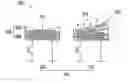
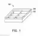
FIG. 1 is a three-dimensional schematic diagram of a pressure sensor according to an embodiment of the invention.
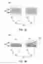
FIG. 2A is a cross-sectional schematic diagram of the pressure sensor of FIG. 1 not under pressure.
FIG. 2B is a cross-sectional schematic diagram of the pressure sensor of FIG. 2A under pressure.
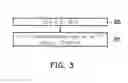
FIG. 3 is a manufacturing flow chart of a pressure sensor according to another embodiment of the invention.
DESCRIPTION OF THE EMBODIMENTS
FIG. 1 is a three-dimensional schematic diagram of a pressure sensor according to an embodiment of the invention.
Please refer to FIG. 1. A pressure sensor 100 of the present embodiment includes a thin-film transistor array 102 and a pressure-sensitive layer 104 covering the thin-film transistor array 102. The pressure-sensitive layer 104 is, for instance, inductive resistive.
Hereinafter, the detailed structure of the pressure sensor of FIG. 1 and embodiments thereof are exemplarily described with reference to FIG. 2A and FIG. 2B.
Please refer first to FIG. 2A. The pressure sensor 100 of the present embodiment includes a thin-film transistor array 102 and a pressure-sensitive layer 104 covering the thin-film transistor array 102. The pressure-sensitive layer 104 includes a plurality of one-dimensional materials 206 arranged on the same plane and a plurality of insulating layers 208, and the one-dimensional materials 206 and the insulating layers 208 are alternately stacked, such that the one-dimensional materials 206 between the layers are not in contact with one another.
In the present embodiment, the diameter of the one-dimensional material is generally 5 nm to 100 nm, preferably 20 nm to 80 nm, and more preferably 40 nm to 60 nm. Moreover, in terms of good conductivity, the length of the one-dimensional material is not particularly limited provided the aspect ratio of the one-dimensional material is greater than 100. For instance, the one-dimensional material may include a metal nanowire, a carbon nanotube, or a metal oxide semiconductor. The metal of the metal nanowire may include gold, silver, or copper, but is not limited thereto. The metal oxide of the metal oxide semiconductor may include zinc oxide, titanium oxide, tungsten oxide, molybdenum oxide, vanadium oxide, copper oxide, nickel oxide, cobalt oxide, iron oxide, or tin oxide, but is not limited thereto.
In FIG. 2A and FIG. 2B, for ease of illustration, only two adjacent thin-film transistor elements (a first thin-film transistor element 210 and a second thin-film transistor element 212) are shown, but it should be understood that, the thin-film transistor array may contain more thin-film transistor elements and is not limited to the quantity shown in FIG. 2A or FIG. 2B.
When pressure is not applied, as shown in FIG. 2A, since the one-dimensional materials 206 on the first thin-film transistor element 210 and the second thin-film transistor element 212 are separated by the insulating layers 208, current is not readily transferred between the one-dimensional materials 206, and therefore the one-dimensional materials 206 are in high-resistance state. When a pressure 214 is applied to a region of the first thin-film transistor element 210, as shown in FIG. 2B, the distances between the one-dimensional materials 206 are decreased due to the deformation of the pressure-sensitive layer 104 on the first thin-film transistor element 210 from pressure. As a result, current is readily transferred between the one-dimensional materials 206, such that the resistance of the pressure-sensitive layer 104 is reduced. Moreover, although the pressure-sensitive layer 104 on the second thin-film transistor element 212 is also deformed due to the pressure 214, even if deformation occurs, the one-dimensional materials 206 having directionality do not readily come in contact with one another since the pressure-sensitive layer 104 is not directly located on the point of application. Therefore, in the pressure-sensitive layer 104, the region 216 away from the point of application still has high resistance. Therefore, in comparison to conventional pressure sensor in which the pressure-sensitive layer contains conductive particles, the invention may provide better pressure resolution and may be applied in a pressure image sensing technique such as fingerprint recognition or foot pressure sensing, but is not limited thereto. The invention may be applied in any situation requiring pressure sensing.
Moreover, the one-dimensional materials 206 may also be replaced by two-dimensional materials (not shown) such that a pressure-sensitive layer is formed by the alternate stacking of the two-dimensional materials and the insulating layers 208. The two-dimensional materials may include, for instance, graphene oxide or molybdenum disulfide (MoS2), but is not limited thereto. The structure of the two-dimensional materials may also be alternately stacked with the insulating layers 208 to prevent contact of the two-dimensional materials between the layers. Therefore, the embodiment thereof is similar to that of the one-dimensional materials and is therefore not repeated herein.
Hereinafter, the manufacturing method of the pressure sensor according to another embodiment of the invention is described. Please refer to FIG. 3.
First, step 300 is performed to form a TFT (thin-film transistor) array, and the method of forming the TFT array may adopt any known manufacturing method.
Then, step 302 is performed to form a pressure-sensitive layer on the TFT array by 3D printing, wherein the pressure-sensitive layer includes insulating layers and one-dimensional materials arranged on the same plane, and the insulating layers and the one-dimensional materials are alternately stacked. In other embodiment, the pressure-sensitive layer includes insulating layers and two-dimensional materials, and the insulating layers and the two-dimensional materials are alternately stacked. The one-dimensional materials and the two-dimensional materials are as described in each of the embodiments above and are therefore not repeated herein. When the pressure-sensitive layer is a one-dimensional material, the insulating layers and the one-dimensional materials are alternately formed on the TFT array, and therefore the one-dimensional materials between the layers do not come in contact in the absence of pressure, and current is transferred between the one-dimensional materials only after the pressure-sensitive layer is subjected to a certain amount of pressure to change (reduce) the resistance of the pressure sensor.
When the pressure-sensitive layer includes two-dimensional materials, the insulating layers and the two-dimensional materials are similarly alternately formed on the TFT array, and the results thereof are the same as those of the pressure-sensitive layer formed by one-dimensional materials.
Moreover, in addition to the 3D printing, the method of forming the pressure-sensitive layer may also adopt a manufacturing method suitable for roll-to-roll such as screen printing or gravure printing.
Based on the above, in the pressure sensor of the invention, by alternately stacking the plurality of one-dimensional materials arranged on the same plane and the insulating layers or alternately stacking the plurality of two-dimensional materials and the insulating layers in the pressure-sensitive layer, the pressure resolution of the pressure sensor may be enhanced. The reason is that, current transfer between the one-dimensional materials or two-dimensional materials has directionality, and therefore in comparison to conventional pressure sensor in which the pressure-sensitive layer contains conductive particles, the invention may provide better pressure resolution.
Although the invention has been described with reference to the above embodiments, it will be apparent to one of ordinary skill in the art that modifications to the described embodiments may be made without departing from the spirit of the invention. Accordingly, the scope of the invention is defined by the attached claims not by the above detailed descriptions.
Claims
What is claimed is:1. A pressure sensor, comprising:
a thin-film transistor array; and
a pressure-sensitive layer covering the thin-film transistor array, wherein the pressure-sensitive layer comprises a plurality of one-dimensional materials arranged on the same plane and a plurality of insulating layers, and the one-dimensional materials and the insulating layers are alternately stacked.
2. The pressure sensor of claim 1, wherein the pressure-sensitive layer is inductive resistive.
3. The pressure sensor of claim 1, wherein a diameter of the one-dimensional material is 5 nm to 100 mm.
4. The pressure sensor of claim 1, wherein an aspect ratio of the one-dimensional material is greater than 100.
5. The pressure sensor of claim 1, wherein the one-dimensional material comprises a metal nanowire, a carbon nanotube, or a metal oxide semiconductor.
6. The pressure sensor of claim 5, wherein a metal of the metal nanowire comprises gold, silver, or copper.
7. The pressure sensor of claim 5, wherein a metal oxide of the metal oxide semiconductor comprises zinc oxide, titanium oxide, tungsten oxide, molybdenum oxide, vanadium oxide, copper oxide, nickel oxide, cobalt oxide, iron oxide, or tin oxide.
8. A pressure sensor, comprising:
a thin-film transistor array; and
a pressure-sensitive layer covering the thin-film transistor array, wherein the pressure-sensitive layer comprises a plurality of two-dimensional materials and a plurality of insulating layers, and the two-dimensional materials and the insulating layers are alternately stacked.
9. The pressure sensor of claim 8, wherein the two-dimensional material comprises graphene oxide or molybdenum disulfide.
10. The pressure sensor of claim 8, wherein the pressure-sensitive layer is inductive resistive.
11. A manufacturing method of a pressure sensor, comprising:
forming a thin-film transistor array; and
teaming a pressure-sensitive layer on the thin-film transistor array by 3D printing, wherein the pressure-sensitive layer comprises a plurality of insulating layers and a plurality of one-dimensional materials arranged on the same plane that are alternately stacked, or the pressure-sensitive layer comprises the plurality of insulating layers and a plurality of two-dimensional materials that are alternately stacked.
12. The manufacturing method of the pressure sensor of claim 11, wherein a diameter of the one-dimensional material is 5 nm to 100 mm.
13. The manufacturing method of the pressure sensor of claim 11, wherein an aspect ratio of the one-dimensional material is greater than 100.
14. The manufacturing method of the pressure sensor of claim 11, wherein the one-dimensional material comprises a metal nanowire, a carbon nanotube, or a metal oxide semiconductor, and the two-dimensional material comprises graphene oxide or molybdenum disulfide.
15. The manufacturing method of the pressure sensor of claim 14, wherein a metal of the metal nanowire comprises gold, silver, or copper, and a metal oxide of the metal oxide semiconductor comprises zinc oxide, titanium oxide, tungsten oxide, molybdenum oxide, vanadium oxide, copper oxide, nickel oxide, cobalt oxide, iron oxide, or tin oxide.
Images & Drawings included:
Sources:
- United States Patent and Trademark Office - verify current appl. status at the USPTO↗
Similar patent applications:
- » 20130327149
Capacitive pressure sensor, manufacturing method thereof, and pressure sensor package - » 20200309629
Pressure sensor, manufacturing method thereof, pressure sensing method and display device - » 20220155169
Capacitive pressure sensor, manufacturing method thereof, and capacitive pressure sensor device - » 20240426680
PRESSURE SENSOR, MANUFACTURING METHOD THEREOF AND PRESSURE DETECTION DEVICE - » 20110152694
BLOOD-PRESSURE SENSOR, MANUFACTURING METHOD THEREOF, AND BLOOD-PRESSURE SENSOR SYSTEM - » 20080178681
Semiconductor pressure sensor, manufacturing method thereof, and die for molding semiconductor pressure sensor - » 20200309619
Pressure sensor, manufacturing method thereof, and electronic device - » 20090266170
Pressure sensor, manufacturing method thereof, and electronic component provided therewith - » 20190154533
Pressure sensor, manufacturing method thereof, and display device having the same - » 20230175911
Pressure sensor, manufacturing method thereof, and display device having the same
Recent applications in this class:
- » 20230066181 2023-03-02
Modular actuating device, vehicle, and method - » 20200333203 2020-10-22
Coil actuated pressure sensor and deformable substrate
Recent applications for this Assignee:
- » 20250287621 2025-09-11
3D CAPACITANCE STRUCTURE AND MANUFACTURE METHOD THEREOF - » 20250287616 2025-09-11
SEMICONDUCTOR STRUCTURE AND MANUFACTURING METHOD THEREOF - » 20250287585 2025-09-11
MANUFACTURING METHOD OF SEMICONDUCTOR STRUCTURE - » 20250286558 2025-09-11
DELAY CONTROL METHOD - » 20250285673 2025-09-11
SEMICONDUCTOR MEMORY DEVICE AND METHOD FOR CONTROLLING THE SAME - » 20250284465 2025-09-11
TRUE RANDOM NUMBER GENERATOR AND TRUE RANDOM NUMBER GENERATING METHOD THEREOF - » 20250273264 2025-08-28
MEMORY ARRAY AND MEMORY CELL - » 20250272849 2025-08-28
METHOD FOR DETECTING IMAGE BOUNDARY USING GAN MODEL, COMPUTER READABLE RECORDING MEDIA, AND ELECTRONIC APPARATUS - » 20250271495 2025-08-28
CHIP TEST SYSTEM AND METHOD - » 20250267851 2025-08-21
SEMICONDUCTOR STRUCTURE AND METHOD FOR FORMING THE SAME