BOA liquid crystal panel based on IGZO-TFT and method for manufacturing the same
US20180210298A1
2018-07-26
15/328,920
2017-01-05
✅ Patent granted
US 10,191,339 B2
2019-01-29
WO; PCT/CN2017/070280; 20170105
WO; WO2018/040464; 20180308
Dung Le
2037-01-05
Abstract:
Provided is a BOA liquid crystal panel based on an IGZO-TFT and a method for manufacturing the same. The method includes steps of: (1) forming a black matrix; (2) forming a gate; (3) forming a gate insulator; (4) forming a source and a drain; (5) forming IGZO; (6) forming a passivation; (7) forming R/G/B color resist; (8) forming ITO. Copper oxide is used as a coplanar structure of the black matrix of an IGZO-TFT based BOA component, which can effectively prevent the risk of etching IGZO.
Assignee:
- Shenzhen China Star Optoelectronics Technology Co Ltd. 3,202 🇨🇳 Shenzhen, Guangdong, China
- SHENZHEN CHINA STAR OPTOELECTRONICS TECHNOLOGY CO., LTD. 1,397 🇨🇳 Shenzhen, China
Applicant:
Interested in similar patents?
Get notified when new applications in this technology area are published.
Classification:
G02F1/136209 » CPC main
Devices or arrangements for the control of the intensity, colour, phase, polarisation or direction of light arriving from an independent light source, e.g. switching, gating or modulating; Non-linear optics for the control of the intensity, phase, polarisation or colour based on liquid crystals, e.g. single liquid crystal display cells; Constructional arrangements; Operation of liquid crystal cells; Circuit arrangements; Liquid crystal cells structurally associated with a semi-conducting layer or substrate, e.g. cells forming part of an integrated circuit; Active matrix addressed cells Light shielding layers, e.g. black matrix, incorporated in the active matrix substrate, e.g. structurally associated with the switching element
H01L21/0274 » CPC further
Processes or apparatus adapted for the manufacture or treatment of semiconductor or solid state devices or of parts thereof; Manufacture or treatment of semiconductor devices or of parts thereof; Making masks on semiconductor bodies for further photolithographic processing not provided for in group or comprising organic layers characterised by the treatment of photoresist layers Photolithographic processes
H01L21/02565 » CPC further
Processes or apparatus adapted for the manufacture or treatment of semiconductor or solid state devices or of parts thereof; Manufacture or treatment of semiconductor devices or of parts thereof; Forming layers; Forming inorganic semiconducting materials on a substrate; Deposited layers; Materials Oxide semiconducting materials not being Group 12/16 materials, e.g. ternary compounds
H01L21/02631 » CPC further
Processes or apparatus adapted for the manufacture or treatment of semiconductor or solid state devices or of parts thereof; Manufacture or treatment of semiconductor devices or of parts thereof; Forming layers; Forming inorganic semiconducting materials on a substrate; Formation types; Deposition types Physical deposition at reduced pressure, e.g. MBE, sputtering, evaporation
H01L27/127 » CPC further
Devices consisting of a plurality of semiconductor or other solid-state components formed in or on a common substrate including semiconductor components specially adapted for rectifying, oscillating, amplifying or switching and having at least one potential-jump barrier or surface barrier; including integrated passive circuit elements with at least one potential-jump barrier or surface barrier the substrate being other than a semiconductor body, e.g. an insulating body comprising a plurality of TFTs formed on a non-semiconducting substrate, e.g. driving circuits for AMLCDs; Multistep manufacturing methods with a particular formation, treatment or patterning of the active layer specially adapted to the circuit arrangement
H01L27/1225 » CPC further
Devices consisting of a plurality of semiconductor or other solid-state components formed in or on a common substrate including semiconductor components specially adapted for rectifying, oscillating, amplifying or switching and having at least one potential-jump barrier or surface barrier; including integrated passive circuit elements with at least one potential-jump barrier or surface barrier the substrate being other than a semiconductor body, e.g. an insulating body comprising a plurality of TFTs formed on a non-semiconducting substrate, e.g. driving circuits for AMLCDs with a particular composition, shape or crystalline structure of the active layer with semiconductor materials not belonging to the group IV of the periodic table, e.g. InGaZnO
H01L27/1262 » CPC further
Devices consisting of a plurality of semiconductor or other solid-state components formed in or on a common substrate including semiconductor components specially adapted for rectifying, oscillating, amplifying or switching and having at least one potential-jump barrier or surface barrier; including integrated passive circuit elements with at least one potential-jump barrier or surface barrier the substrate being other than a semiconductor body, e.g. an insulating body comprising a plurality of TFTs formed on a non-semiconducting substrate, e.g. driving circuits for AMLCDs; Multistep manufacturing methods with a particular formation, treatment or coating of the substrate
H01L29/437 » CPC further
Semiconductor devices adapted for rectifying, amplifying, oscillating or switching, or capacitors or resistors with at least one potential-jump barrier or surface barrier, e.g. PN junction depletion layer or carrier concentration layer; Details of semiconductor bodies or of electrodes thereof; Multistep manufacturing processes therefor; Electrodes ; Multistep manufacturing processes therefor characterised by the materials of which they are formed Superconductor materials
H01L29/4908 » CPC further
Semiconductor devices adapted for rectifying, amplifying, oscillating or switching, or capacitors or resistors with at least one potential-jump barrier or surface barrier, e.g. PN junction depletion layer or carrier concentration layer; Details of semiconductor bodies or of electrodes thereof; Multistep manufacturing processes therefor; Electrodes ; Multistep manufacturing processes therefor characterised by the materials of which they are formed; Metal-insulator-semiconductor electrodes, e.g. gates of MOSFET for thin film semiconductor, e.g. gate of TFT
H01L29/66969 » CPC further
Semiconductor devices adapted for rectifying, amplifying, oscillating or switching, or capacitors or resistors with at least one potential-jump barrier or surface barrier, e.g. PN junction depletion layer or carrier concentration layer; Details of semiconductor bodies or of electrodes thereof; Multistep manufacturing processes therefor; Types of semiconductor device ; Multistep manufacturing processes therefor; Multistep manufacturing processes of devices having semiconductor bodies not comprising group 14 or group 13/15 materials
G02F2202/10 » CPC further
Materials and properties semiconductor
H01L27/108 IPC
Devices consisting of a plurality of semiconductor or other solid-state components formed in or on a common substrate including semiconductor components specially adapted for rectifying, oscillating, amplifying or switching and having at least one potential-jump barrier or surface barrier; including integrated passive circuit elements with at least one potential-jump barrier or surface barrier the substrate being a semiconductor body including a plurality of individual components in a repetitive configuration including field-effect components Dynamic random access memory structures
G02F1/1362 » CPC further
Devices or arrangements for the control of the intensity, colour, phase, polarisation or direction of light arriving from an independent light source, e.g. switching, gating or modulating; Non-linear optics for the control of the intensity, phase, polarisation or colour based on liquid crystals, e.g. single liquid crystal display cells; Constructional arrangements; Operation of liquid crystal cells; Circuit arrangements; Liquid crystal cells structurally associated with a semi-conducting layer or substrate, e.g. cells forming part of an integrated circuit Active matrix addressed cells
G02F1/1368 » CPC further
Devices or arrangements for the control of the intensity, colour, phase, polarisation or direction of light arriving from an independent light source, e.g. switching, gating or modulating; Non-linear optics for the control of the intensity, phase, polarisation or colour based on liquid crystals, e.g. single liquid crystal display cells; Constructional arrangements; Operation of liquid crystal cells; Circuit arrangements; Liquid crystal cells structurally associated with a semi-conducting layer or substrate, e.g. cells forming part of an integrated circuit; Active matrix addressed cells in which the switching element is a three-electrode device
H01L21/02 IPC
Processes or apparatus adapted for the manufacture or treatment of semiconductor or solid state devices or of parts thereof Manufacture or treatment of semiconductor devices or of parts thereof
H01L21/027 IPC
Processes or apparatus adapted for the manufacture or treatment of semiconductor or solid state devices or of parts thereof; Manufacture or treatment of semiconductor devices or of parts thereof Making masks on semiconductor bodies for further photolithographic processing not provided for in group or
H01L21/443 » CPC further
Processes or apparatus adapted for the manufacture or treatment of semiconductor or solid state devices or of parts thereof; Manufacture or treatment of semiconductor devices or of parts thereof the devices having at least one potential-jump barrier or surface barrier, e.g. PN junction, depletion layer or carrier concentration layer the devices having semiconductor bodies not provided for in groups, , , and with or without impurities, e.g. doping materials; Manufacture of electrodes on semiconductor bodies using processes or apparatus not provided for in groups - ; Deposition of conductive or insulating materials for electrodes from a gas or vapour, e.g. condensation
H01L21/4763 IPC
Processes or apparatus adapted for the manufacture or treatment of semiconductor or solid state devices or of parts thereof; Manufacture or treatment of semiconductor devices or of parts thereof the devices having at least one potential-jump barrier or surface barrier, e.g. PN junction, depletion layer or carrier concentration layer the devices having semiconductor bodies not provided for in groups, , , and with or without impurities, e.g. doping materials; Treatment of semiconductor bodies using processes or apparatus not provided for in groups to change their surface-physical characteristics or shape, e.g. etching, polishing, cutting Deposition of non-insulating, e.g. conductive -, resistive -, layers on insulating layers; After-treatment of these layers
H01L27/12 IPC
Devices consisting of a plurality of semiconductor or other solid-state components formed in or on a common substrate including semiconductor components specially adapted for rectifying, oscillating, amplifying or switching and having at least one potential-jump barrier or surface barrier; including integrated passive circuit elements with at least one potential-jump barrier or surface barrier the substrate being other than a semiconductor body, e.g. an insulating body
H01L29/423 IPC
Semiconductor devices adapted for rectifying, amplifying, oscillating or switching, or capacitors or resistors with at least one potential-jump barrier or surface barrier, e.g. PN junction depletion layer or carrier concentration layer; Details of semiconductor bodies or of electrodes thereof; Multistep manufacturing processes therefor; Electrodes ; Multistep manufacturing processes therefor characterised by their shape, relative sizes or dispositions not carrying the current to be rectified, amplified or switched
H01L29/43 IPC
Semiconductor devices adapted for rectifying, amplifying, oscillating or switching, or capacitors or resistors with at least one potential-jump barrier or surface barrier, e.g. PN junction depletion layer or carrier concentration layer; Details of semiconductor bodies or of electrodes thereof; Multistep manufacturing processes therefor; Electrodes ; Multistep manufacturing processes therefor characterised by the materials of which they are formed
H01L29/49 IPC
Semiconductor devices adapted for rectifying, amplifying, oscillating or switching, or capacitors or resistors with at least one potential-jump barrier or surface barrier, e.g. PN junction depletion layer or carrier concentration layer; Details of semiconductor bodies or of electrodes thereof; Multistep manufacturing processes therefor; Electrodes ; Multistep manufacturing processes therefor characterised by the materials of which they are formed Metal-insulator-semiconductor electrodes, e.g. gates of MOSFET
H01L29/66 IPC
Semiconductor devices adapted for rectifying, amplifying, oscillating or switching, or capacitors or resistors with at least one potential-jump barrier or surface barrier, e.g. PN junction depletion layer or carrier concentration layer; Details of semiconductor bodies or of electrodes thereof; Multistep manufacturing processes therefor Types of semiconductor device ; Multistep manufacturing processes therefor
H01L29/786 IPC
Semiconductor devices adapted for rectifying, amplifying, oscillating or switching, or capacitors or resistors with at least one potential-jump barrier or surface barrier, e.g. PN junction depletion layer or carrier concentration layer; Details of semiconductor bodies or of electrodes thereof; Multistep manufacturing processes therefor; Types of semiconductor device ; Multistep manufacturing processes therefor controllable by only the electric current supplied, or only the electric potential applied, to an electrode which does not carry the current to be rectified, amplified or switched; Unipolar devices, e.g. field effect transistors; Field effect transistors with field effect produced by an insulated gate Thin film transistors, i.e. transistors with a channel being at least partly a thin film
Description
FIELD OF THE INVENTION
The present disclosure relates to the field of liquid crystal, and in particularly to a BOA liquid crystal panel based on an IGZO-TFT and a method for manufacturing the same.
BACKGROUND OF THE INVENTION
Black matrix on array (BOA) technique is a popular technique for manufacturing a liquid crystal display (LCD) panel. In a BOA process, a color filter (CF) substrate is not used, which renders a CF process unnecessary and can reduce costs, improve the alignment precision of the manufacturing process, and is conducive to manufacture of display devices of high aperture ratio and high resolution.
In a traditional BOA process, a black matrix (BM) is an organic photoresist, and patterning is performed after coating of R/G/B color resist. Since the BM has a high requirement for optical density, but the optical density of the existing BM for a BOA structure is low, a coating of the BM is extremely thick. However, the thick BM coating can shield alignment marks on the array substrate, which is not conducive to exposure alignment in the process. Further, for a BM with large height, it is difficult to control a taper angle thereof and the taper angle is relatively steep, which may cause breakage of pixel indium tin oxide (ITO; ITO is an N-type oxide semiconductor, and ITO thin film is indium tin oxide semiconductor transparent conductive film) when ITO laps on the BM.
Metal oxides have good insulativity. However, many metal oxides, especially those materials that are widely used in industrial applications, such as aluminum oxide (Al2O3), have good transmissivity, and are not suitable for use as a BM material. The inventors of the present disclosure found that copper oxide (CuO) as a black oxide is easily used in industrial production and can be used as a BM material.
IGZO (indium gallium zinc oxide, a metal oxide) is a good material for an active layer of a thin film transistor (TFT) because of its high mobility, good film formation uniformity, easiness in large-size production, and because it can be applied in the same manufacturing process as arsenic (As). In recent years, IGZO has been widely developed. Similar to ITO, IGZO is easy to be etched by aluminum hydroxide (Al(OH)3), so it is generally not suitable for use as a component with a back channel etched (BCE) structure. This is because, in a BCE structure, an IGZO layer is etched away when a source and a drain are formed by etching, which can result in failure in the manufacture of the TFT component.
In view of the foregoing, the inventors of the present disclosure designed a BOA liquid crystal panel based on an IGZO-TFT and a method for manufacturing the same to eliminate the above-mentioned defect.
SUMMARY OF THE INVENTION
It is an object of the present disclosure to provide a BOA liquid crystal panel based on an IGZO-TFT and a method for manufacturing the same. In the present disclosure, copper oxide is used as a coplanar structure of a black matrix of a IGZO-TFT based BOA component, which effectively prevents the risk of etching IGZO.
In order to achieve the above object, the present disclosure provides a method for manufacturing a BOA liquid crystal panel based on an IGZO-TFT. The method comprising steps of:
(1) forming a black matrix, which comprises:
forming a copper film on a substrate,
oxidizing the copper film to obtain a copper oxide film, and
patterning the copper oxide film and exposing an opening area to obtain a black matrix pattern;
(2) forming a gate, which comprises forming a gate film on the black matrix pattern, and then exposing the gate film to radiation to obtain a gate pattern;
(3) forming a gate insulator), which comprises forming a gate insulator film on the resulting structure of step (2) to form a gate insulator film;
(4) forming a source and a drain, which comprises forming a source film and a drain film on a part of the gate insulator film which covers the gate pattern, and then exposing the source film and the drain film to obtain a source pattern and a drain pattern;
(5) forming IGZO, which comprises forming a IGZO film on a part of the gate insulator film which covers the gate pattern and is between the source and the drain to obtain an IGZO pattern;
(6) forming a passivation, which comprises forming a passivation film on the resulting structure of step (5), and forming a contact hole passing through the passivation film on the source and the drain;
(7) forming R/G/B color resist, which comprises coating the resulting structure of step (6) except the contact hole, with R/G/B color resist, and exposing the coating to radiation to obtain a desired pattern;
(8) forming ITO, which comprises covering the contact hole and the opening area with an ITO film, and exposing the ITO film to radiation to obtain an ITO pattern.
According to the method for manufacturing a BOA liquid crystal panel based on an IGZO-TFT, in step (1), the copper film is formed by physical vapor deposition.
According to the method for manufacturing a BOA liquid crystal panel based on an IGZO-TFT, in step (2), the gate film is formed by physical vapor deposition, and the gate pattern is obtained by subjecting the gate film to exposure and to dry etching. The gate pattern is made of copper.
According to the method for manufacturing a BOA liquid crystal panel based on an IGZO-TFT, in step (3), the gate insulator film is formed by chemical vapor deposition, and the gate insulator film is made of silicon dioxide.
According to the method for manufacturing a BOA liquid crystal panel based on an IGZO-TFT, in step (4), the source film and the drain film are formed by physical vapor deposition, and the source pattern and the drain pattern are obtained by subjecting the source film and the drain film to exposure and to wet etching, and the source pattern and the drain pattern are made of copper
According to the method for manufacturing a BOA liquid crystal panel based on an IGZO-TFT, in step (5), the metal oxide IGZO film is formed by physical vapor deposition, and the IGZO pattern is obtained by subjecting the IGZO film to exposure and to wet etching.
According to the method for manufacturing a BOA liquid crystal panel based on an IGZO-TFT, in step (6), the passivation film is formed by chemical vapor deposition, and the passivation film is made of SiO2.
According to the method for manufacturing a BOA liquid crystal panel based on an IGZO-TFT, in step (8), the ITO film is formed by physical vapor deposition, and the pattern is obtained by subjecting the ITO film to exposure and to wet etching.
The present disclosure further provides a BOA liquid crystal panel based on an IGZO-TFT. The liquid crystal panel mainly comprises a substrate having a BM pattern thereon. An opening area of the BM pattern is exposed. The BM pattern has a gate pattern thereon. The substrate, the BM pattern, and the gate pattern have a gate insulator film thereon. The gate pattern covered by the gate insulator film has a source and a drain thereon. An IGZO film is provided on a part of the gate insulator film which covers the gate pattern covered and is between the source and the drain. A passivation film is provided on the whole resulting structure, and the passivation film has a contact hole at a position corresponding to the source and the drain. R/G/B color resist is applied to the entire resulting structure, except the contact hole. The contact hole and the opening area are covered with an ITO pattern.
In the BOA liquid crystal panel based on an IGZO-TFT, the black matrix pattern is formed of copper oxide.
The present disclosure brings the following beneficial effects. The present disclosure provides an IGZO-TFT based BOA component using CuO as the coplanar structure of a BM, and effectively overcomes the difficulty of the prior art in manufacturing a BM of a BOA structure, and in etching IGZO in the BCE structure in the IGZO-TFT. In addition, the present disclosure adopts a bottom-gate structure (coplanar), so that a source and a drain can be formed before the formation of IGZO, whereby the risk of etching IGZO can be avoided.
BRIEF DESCRIPTION OF THE DRAWINGS
The present disclosure will be described in more detail below by way of embodiments and with reference to the accompanying drawings, in which:
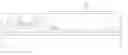
FIG. 1 is a schematic diagram of manufacturing a BM pattern;
FIG. 2 is a schematic diagram of manufacturing a gate pattern;
FIG. 3 is a schematic diagram of manufacturing a GI (gate insulator) film;
FIG. 4 is a schematic diagram of manufacturing a source and a drain;
FIG. 5 is a schematic diagram of manufacturing an IGZO film;
FIG. 6 is a schematic diagram of manufacturing a PV (passivation) film;
FIG. 7 is a schematic diagram of manufacturing R/G/B color resist; and
FIG. 8 is a schematic diagram of manufacturing an ITO pattern.
In the drawings, same reference numerals are used for same parts. The drawings are not provided by an actual proportion.
DETAILED DESCRIPTION OF THE EMBODIMENTS
The present disclosure will be further described below with reference to the accompanying drawings.
The present disclosure provides a method for manufacturing a BOA liquid crystal panel based on an IGZO-TFT. The method comprises the following steps.
(1) Forming a Black Matrix (BM):
As shown in FIG. 1, first, a copper (Cu) film is formed on a substrate 1 by physical vapor deposition (PVD) followed by O2 plasma treatment to obtain a copper oxide (CuO) layer. That is to say, the copper oxide layer is used as a barrier layer of a BM for patterning, and an opening area 3 is exposed. Then the copper oxide layer is exposed to radiation, and subjected to wet etching to obtain a BM pattern 2. It needs to be noted that only the opening area 3 of the BM pattern is exposed.
(2) Forming a Gate:
As shown in FIG. 2, a gate film is formed on the BM pattern 2 by PVD, and then the gate film is exposed to radiation, and subjected to dry etching to obtain a gate pattern 4. Preferably,the gate pattern 4 is made of copper (Cu).
(3) Forming a GI (Gate Insulator):
As shown in FIG. 3, a GI film formed by chemical vapor deposition (CVD) on the entire surface of the substrate. Preferably, the GI film 5 is made of silicon dioxide (SiO2).
(4) Forming a Source and a Drain:
As shown in FIG. 4, a source film and a drain film are formed on a part of the GI film 5 which covers the gate pattern 4 by PVD, and then the source film and the drain film are exposed to radiation and subjected to wet etching to obtain a source and a drain pattern. Preferably, the source and the drain pattern 6 are made of copper (Cu).
(5) Forming a Metal Oxide:
As shown in FIG. 5, a metal oxide (IGZO) film is formed on a part of the GI film 5 which covers the gate pattern 4 and which is between the source and the drain 6 by PVD, and then the metal oxide film is exposed to radiation and subjected to wet etching to obtain a metal oxide (IGZO) pattern 7.
(6) Forming a PV (Passivation):
As shown in FIG. 6, a PV film 8 is formed by CVD on the entire resulting structure, and a contact hole 9 of pixel passing through the PV film 8 and located on the source and the drain pattern 6 is obtained by dry etching. Preferably,the PV film is made of SiO2.
(7) Forming R/G/B Color Resist:
As shown in FIG. 7, the resulting structure, except the contact hole, is coated with R/G/B color resist and is exposed radiation to obtain a desired pattern.
(8) Forming ITO (Indium Tin Oxide):
As shown in FIG. 8, an ITO film is formed to cover the contact hole 9 and the opening region 3 by PVD, and the ITO film is then exposed to radiation and subjected to wet etching to obtain an ITO pattern 11.
The present disclosure further provides a BOA liquid crystal panel based on an IGZO-TFT. The liquid crystal panel mainly comprises, as shown in FIG. 8, a substrate 1 having a BM pattern 2 thereon. An opening area 3 of the BM pattern 2 is exposed. The BM pattern has a gate pattern 4 thereon. The substrate 1, the BM pattern 2, and the gate pattern 4 have a GI film 5 thereon. The gate pattern 4 covered by the GI film 5 has a source and a drain 6 thereon. An IGZO film 7 is provided on the gate pattern 4 covered by the GI film and between the source and the drain 6. A PV film 8 is provided on the whole resulting structure, and the PV film 8 has a contact hole 9 at a position corresponding to the source and the drain 6. R/G/B color resist 10 is applied to the entire resulting structure, except the contact hole 9. The contact hole 9 and the opening area 3 are covered with an ITO pattern 11.
In view of the above, the present disclosure brings the following beneficial effects.
The present disclosure provides an IGZO-TFT based BOA component using CuO as the coplanar structure of a BM, and effectively overcomes the difficulty of the prior art in manufacturing a BM of a BOA structure, and in etching IGZO in the BCE structure in the IGZO-TFT. In addition, the present disclosure adopts a bottom-gate structure (coplanar), so that a source and a drain can be formed before the formation of IGZO, whereby the risk of etching IGZO can be avoided.
Although the present disclosure has been described with reference to preferred embodiments, various modifications may be made thereto without departing from the scope of the present disclosure, and equivalents may be used for replacing the components therein. In particular, the technical features mentioned in the various embodiments may be combined in any manner as long as there is no structural conflict. The present disclosure is not limited to the specific embodiments disclosed herein, but includes all the technical solutions falling within the scope of the claims.
Claims
1. A method for manufacturing a BOA liquid crystal panel based on an IGZO-TFT, comprising steps of:
(1) forming a black matrix, which comprises:
forming a copper film on a substrate,
oxidizing the copper film to obtain a copper oxide film, and
patterning the copper oxide film and exposing an opening area to obtain a black matrix pattern;
(2) forming a gate, which comprises forming a gate film on the black matrix pattern, and then exposing the gate film to radiation to obtain a gate pattern;
(3) forming a gate insulator, which comprises forming a gate insulator film on the resulting structure of step (2) to form a gate insulator film;
(4) forming a source and a drain, which comprises forming a source film and a drain film on a part of the gate insulator film which covers the gate pattern, and then exposing the source and the drain film to obtain a source and a drain pattern;
(5) forming IGZO, which comprises forming a IGZO film on a part of the gate insulator film which covers the gate pattern and is between the source and the drain to obtain an IGZO pattern;
(6) forming a passivation, which comprises forming a passivation film on the resulting structure of step (5), and forming a contact hole passing through the passivation film on the source and the drain;
(7) forming R/G/B color resist, which comprises coating the resulting structure of step (6) except the contact hole, with R/G/B color resist, and exposing the coating to radiation to obtain a desired pattern;
(8) forming ITO, which comprises covering the contact hole and the opening area with an ITO film, and exposing the ITO film to radiation to obtain an ITO pattern.
2. The method for manufacturing a BOA liquid crystal panel based on an IGZO-TFT according to claim 1, characterized in that in step (1), the copper film is formed by physical vapor deposition.
3. The method for manufacturing a BOA liquid crystal panel based on an IGZO-TFT according to claim 1, characterized in that in step (2), the gate film is formed by physical vapor deposition, and the gate pattern is obtained by subjecting the gate film to exposure and to dry etching, and the gate pattern is made of copper.
4. The method for manufacturing a BOA liquid crystal panel based on an IGZO-TFT according to claim 1, characterized in that in step (3), the gate insulator film is formed by chemical vapor deposition, and the gate insulator film is made of silicon dioxide.
5. The method for manufacturing a BOA liquid crystal panel based on an IGZO-TFT according to claim 1, characterized in that in step (4), the source and the drain film are formed by physical vapor deposition, and the source pattern and the drain pattern are obtained by subjecting the source film and the drain film to exposure and to wet etching, and the source pattern and the drain pattern are made of copper.
6. The method for manufacturing a BOA liquid crystal panel based on an IGZO-TFT according to claim 1, characterized in that in step (5), the metal oxide IGZO film is formed by physical vapor deposition, and the IGZO pattern is obtained by subjecting the IGZO film to exposure and to wet etching.
7. The method for manufacturing a BOA liquid crystal panel based on an IGZO-TFT according to claim 1, characterized in that in step (6), the PV film is formed by chemical vapor deposition, and the PV film is made of SiO2.
8. The method for manufacturing a BOA liquid crystal panel based on an IGZO-TFT according to claim 1, characterized in that in step (8), the ITO film is formed by physical vapor deposition, and the ITO pattern is obtained by subjecting the ITO film to exposure and to wet etching.
9. A BOA liquid crystal panel based on an IGZO-TFT, comprising a substrate, wherein:
the substrate is provided thereon with a black matrix pattern, an opening area of the black matrix pattern being exposed, and the black matrix pattern being provided thereon with a gate pattern, wherein the substrate, the black matrix pattern, and the gate pattern are provided thereon with a gate insulator film, wherein the gate pattern covered by the gate insulator film is provided thereon with a source and a drain, wherein an IGZO film is provided on a part of the gate insulator film which covers the gate pattern covered and is between the source and the drain, wherein a passivation film is provided on the source and the drain, the IGZO film, and the gate insulator film, wherein the passivation film has a contact hole at a position corresponding to the source and the drain, and the passivation film, except the contact hole, is coated with R/G/B color resist, and the contact hole and the opening area are covered with an ITO pattern.
10. The BOA liquid crystal panel based on an IGZO-TFT according to claim 9, characterized in that the black matrix pattern is formed of copper oxide.
Images & Drawings included:


Sources:
- United States Patent and Trademark Office - verify current appl. status at the USPTO↗
Recent applications in this class:
- » 20250271712 2025-08-28
ELECTRONIC DEVICE - » 20250271711 2025-08-28
PIXEL STRUCTURE - » 20250264769 2025-08-21
DISPLAY PANEL - » 20250216730 2025-07-03
ELECTRO-OPTICAL DEVICE AND ELECTRONIC APPARATUS - » 20250216729 2025-07-03
ELECTRO-OPTICAL DEVICE AND ELECTRONIC APPARATUS - » 20250199369 2025-06-19
DISPLAY DEVICE - » 20250130468 2025-04-24
VR LUMINANCE-OPTIMIZED LCD DESIGN SEEN THROUGH THE LENS - » 20250130467 2025-04-24
LIQUID CRYSTAL DISPLAY DEVICE - » 20250130466 2025-04-24
DISPLAY PANEL - » 20250116904 2025-04-10
ELECTRONIC DEVICE
Recent applications for this Assignee:
- » 20220052204 2022-02-17
Amorphous silicon thin film transistor and method for manufacturing the same - » 20210405424 2021-12-30
Array substrate - » 20210358953 2021-11-18
Pixel structure, array substrate, and display device - » 20210336040 2021-10-28
Manufacturing method of TFT substrate - » 20210335832 2021-10-28
Thin film transistor (TFT) array substrate and display panel - » 20210191204 2021-06-24
Pixel structure and display panel containing same - » 20210090528 2021-03-25
Display driving system - » 20210083229 2021-03-18
OLED display panel and manufacturing method thereof - » 20210083010 2021-03-18
Color filter substrate having a filter layer disposed on quantum dot layer - » 20210082358 2021-03-18
White balance method and device for LCD panel