Array substrate of OLED display device and manufacturing method thereof
US20180212010A1
2018-07-26
15/327,403
2017-01-13
✅ Patent granted
US 10,068,955 B2
2018-09-04
WO; PCT/CN2017/071162; 20170113
-
Tan N Tran
JMD Davis Ben-David
2037-03-14
Abstract:
A manufacturing method of an array substrate of an OLED display device is provided. Active areas of a first thin film transistor T1 and a second thin film transistor T2 are formed by a first mask; channel doping areas, source electrode doping areas and drain electrode doping areas of T1 and T2 are formed by a second mask; gate electrodes of T1 and T2 are formed by a third mask; vias are formed by a fourth mask; source electrodes and drain electrodes of T1 and T2, a data line and a pixel electrode are formed by a fifth mask. The manufacturing method can simplify the process steps.
Assignee:
- SHENZHEN CHINA STAR OPTOELECTRONICS TECHNOLOGY CO., LTD. 1,397 🇨🇳 Shenzhen, China
Applicant:
Interested in similar patents?
Get notified when new applications in this technology area are published.
Classification:
H01L27/124 » CPC further
Devices consisting of a plurality of semiconductor or other solid-state components formed in or on a common substrate including semiconductor components specially adapted for rectifying, oscillating, amplifying or switching and having at least one potential-jump barrier or surface barrier; including integrated passive circuit elements with at least one potential-jump barrier or surface barrier the substrate being other than a semiconductor body, e.g. an insulating body comprising a plurality of TFTs formed on a non-semiconducting substrate, e.g. driving circuits for AMLCDs with a particular composition, shape or layout of the wiring layers specially adapted to the circuit arrangement, e.g. scanning lines in LCD pixel circuits
H01L27/3262 » CPC main
Devices consisting of a plurality of semiconductor or other solid-state components formed in or on a common substrate including components using organic materials as the active part, or using a combination of organic materials with other materials as the active part with components specially adapted for light emission, e.g. flat-panel displays using organic light-emitting diodes [OLED]; Matrix-type displays; Active matrix displays special geometry or disposition of pixel-elements of TFT
H01L21/02631 » CPC further
Processes or apparatus adapted for the manufacture or treatment of semiconductor or solid state devices or of parts thereof; Manufacture or treatment of semiconductor devices or of parts thereof; Forming layers; Forming inorganic semiconducting materials on a substrate; Formation types; Deposition types Physical deposition at reduced pressure, e.g. MBE, sputtering, evaporation
H01L29/66 IPC
Semiconductor devices adapted for rectifying, amplifying, oscillating or switching, or capacitors or resistors with at least one potential-jump barrier or surface barrier, e.g. PN junction depletion layer or carrier concentration layer; Details of semiconductor bodies or of electrodes thereof; Multistep manufacturing processes therefor Types of semiconductor device ; Multistep manufacturing processes therefor
H01L21/76802 » CPC further
Processes or apparatus adapted for the manufacture or treatment of semiconductor or solid state devices or of parts thereof; Manufacture or treatment of devices consisting of a plurality of solid state components formed in or on a common substrate or of parts thereof; Manufacture of integrated circuit devices or of parts thereof; Manufacture of specific parts of devices defined in group; Applying interconnections to be used for carrying current between separate components within a device comprising conductors and dielectrics characterised by the formation and the after-treatment of the dielectrics, e.g. smoothing by forming openings in dielectrics
H01L27/1222 » CPC further
Devices consisting of a plurality of semiconductor or other solid-state components formed in or on a common substrate including semiconductor components specially adapted for rectifying, oscillating, amplifying or switching and having at least one potential-jump barrier or surface barrier; including integrated passive circuit elements with at least one potential-jump barrier or surface barrier the substrate being other than a semiconductor body, e.g. an insulating body comprising a plurality of TFTs formed on a non-semiconducting substrate, e.g. driving circuits for AMLCDs with a particular composition, shape or crystalline structure of the active layer
H01L27/1288 » CPC further
Devices consisting of a plurality of semiconductor or other solid-state components formed in or on a common substrate including semiconductor components specially adapted for rectifying, oscillating, amplifying or switching and having at least one potential-jump barrier or surface barrier; including integrated passive circuit elements with at least one potential-jump barrier or surface barrier the substrate being other than a semiconductor body, e.g. an insulating body comprising a plurality of TFTs formed on a non-semiconducting substrate, e.g. driving circuits for AMLCDs; Multistep manufacturing methods employing particular masking sequences or specially adapted masks, e.g. half-tone mask
H01L27/3248 » CPC further
Devices consisting of a plurality of semiconductor or other solid-state components formed in or on a common substrate including components using organic materials as the active part, or using a combination of organic materials with other materials as the active part with components specially adapted for light emission, e.g. flat-panel displays using organic light-emitting diodes [OLED]; Matrix-type displays; Active matrix displays Connection of the pixel electrode to the TFT
H01L27/3258 » CPC further
Devices consisting of a plurality of semiconductor or other solid-state components formed in or on a common substrate including components using organic materials as the active part, or using a combination of organic materials with other materials as the active part with components specially adapted for light emission, e.g. flat-panel displays using organic light-emitting diodes [OLED]; Matrix-type displays; Active matrix displays Insulating layers formed between TFT elements and OLED elements
H01L27/3276 » CPC further
Devices consisting of a plurality of semiconductor or other solid-state components formed in or on a common substrate including components using organic materials as the active part, or using a combination of organic materials with other materials as the active part with components specially adapted for light emission, e.g. flat-panel displays using organic light-emitting diodes [OLED]; Matrix-type displays; Active matrix displays Wiring lines
H01L29/4908 » CPC further
Semiconductor devices adapted for rectifying, amplifying, oscillating or switching, or capacitors or resistors with at least one potential-jump barrier or surface barrier, e.g. PN junction depletion layer or carrier concentration layer; Details of semiconductor bodies or of electrodes thereof; Multistep manufacturing processes therefor; Electrodes ; Multistep manufacturing processes therefor characterised by the materials of which they are formed; Metal-insulator-semiconductor electrodes, e.g. gates of MOSFET for thin film semiconductor, e.g. gate of TFT
H01L29/49 IPC
Semiconductor devices adapted for rectifying, amplifying, oscillating or switching, or capacitors or resistors with at least one potential-jump barrier or surface barrier, e.g. PN junction depletion layer or carrier concentration layer; Details of semiconductor bodies or of electrodes thereof; Multistep manufacturing processes therefor; Electrodes ; Multistep manufacturing processes therefor characterised by the materials of which they are formed Metal-insulator-semiconductor electrodes, e.g. gates of MOSFET
H01L27/127 » CPC further
Devices consisting of a plurality of semiconductor or other solid-state components formed in or on a common substrate including semiconductor components specially adapted for rectifying, oscillating, amplifying or switching and having at least one potential-jump barrier or surface barrier; including integrated passive circuit elements with at least one potential-jump barrier or surface barrier the substrate being other than a semiconductor body, e.g. an insulating body comprising a plurality of TFTs formed on a non-semiconducting substrate, e.g. driving circuits for AMLCDs; Multistep manufacturing methods with a particular formation, treatment or patterning of the active layer specially adapted to the circuit arrangement
H01L27/1248 » CPC further
Devices consisting of a plurality of semiconductor or other solid-state components formed in or on a common substrate including semiconductor components specially adapted for rectifying, oscillating, amplifying or switching and having at least one potential-jump barrier or surface barrier; including integrated passive circuit elements with at least one potential-jump barrier or surface barrier the substrate being other than a semiconductor body, e.g. an insulating body comprising a plurality of TFTs formed on a non-semiconducting substrate, e.g. driving circuits for AMLCDs with a particular composition or shape of the interlayer dielectric specially adapted to the circuit arrangement
H01L27/1262 » CPC further
Devices consisting of a plurality of semiconductor or other solid-state components formed in or on a common substrate including semiconductor components specially adapted for rectifying, oscillating, amplifying or switching and having at least one potential-jump barrier or surface barrier; including integrated passive circuit elements with at least one potential-jump barrier or surface barrier the substrate being other than a semiconductor body, e.g. an insulating body comprising a plurality of TFTs formed on a non-semiconducting substrate, e.g. driving circuits for AMLCDs; Multistep manufacturing methods with a particular formation, treatment or coating of the substrate
H01L51/5056 » CPC further
Solid state devices using organic materials as the active part, or using a combination of organic materials with other materials as the active part; Processes or apparatus specially adapted for the manufacture or treatment of such devices, or of parts thereof specially adapted for light emission, e.g. organic light emitting diodes [OLED] or polymer light emitting devices [PLED]; Carrier transporting layer Hole transporting layer
H01L2227/323 » CPC further
Indexing scheme for devices consisting of a plurality of semiconductor or other solid state components formed in or on a common substrate covered by group; Devices including an organic light emitting device [OLED], e.g. OLED display Multistep processes for AMOLED
H01L21/00 IPC
Processes or apparatus adapted for the manufacture or treatment of semiconductor or solid state devices or of parts thereof
H01L27/32 IPC
Devices consisting of a plurality of semiconductor or other solid-state components formed in or on a common substrate including components using organic materials as the active part, or using a combination of organic materials with other materials as the active part with components specially adapted for light emission, e.g. flat-panel displays using organic light-emitting diodes [OLED]
H01L21/768 IPC
Processes or apparatus adapted for the manufacture or treatment of semiconductor or solid state devices or of parts thereof; Manufacture or treatment of devices consisting of a plurality of solid state components formed in or on a common substrate or of parts thereof; Manufacture of integrated circuit devices or of parts thereof; Manufacture of specific parts of devices defined in group Applying interconnections to be used for carrying current between separate components within a device comprising conductors and dielectrics
H01L51/56 » CPC further
Solid state devices using organic materials as the active part, or using a combination of organic materials with other materials as the active part; Processes or apparatus specially adapted for the manufacture or treatment of such devices, or of parts thereof specially adapted for light emission, e.g. organic light emitting diodes [OLED] or polymer light emitting devices [PLED] Processes or apparatus specially adapted for the manufacture or treatment of such devices or of parts thereof
H01L21/02 IPC
Processes or apparatus adapted for the manufacture or treatment of semiconductor or solid state devices or of parts thereof Manufacture or treatment of semiconductor devices or of parts thereof
H01L21/306 IPC
Processes or apparatus adapted for the manufacture or treatment of semiconductor or solid state devices or of parts thereof; Manufacture or treatment of semiconductor devices or of parts thereof the devices having at least one potential-jump barrier or surface barrier, e.g. PN junction, depletion layer or carrier concentration layer the devices having semiconductor bodies comprising elements of Group IV of the Periodic System or AB compounds with or without impurities, e.g. doping materials; Treatment of semiconductor bodies using processes or apparatus not provided for in groups - to change their surface-physical characteristics or shape, e.g. etching, polishing, cutting Chemical or electrical treatment, e.g. electrolytic etching
H01L29/786 IPC
Semiconductor devices adapted for rectifying, amplifying, oscillating or switching, or capacitors or resistors with at least one potential-jump barrier or surface barrier, e.g. PN junction depletion layer or carrier concentration layer; Details of semiconductor bodies or of electrodes thereof; Multistep manufacturing processes therefor; Types of semiconductor device ; Multistep manufacturing processes therefor controllable by only the electric current supplied, or only the electric potential applied, to an electrode which does not carry the current to be rectified, amplified or switched; Unipolar devices, e.g. field effect transistors; Field effect transistors with field effect produced by an insulated gate Thin film transistors, i.e. transistors with a channel being at least partly a thin film
H01L27/12 IPC
Devices consisting of a plurality of semiconductor or other solid-state components formed in or on a common substrate including semiconductor components specially adapted for rectifying, oscillating, amplifying or switching and having at least one potential-jump barrier or surface barrier; including integrated passive circuit elements with at least one potential-jump barrier or surface barrier the substrate being other than a semiconductor body, e.g. an insulating body
H01L51/50 IPC
Solid state devices using organic materials as the active part, or using a combination of organic materials with other materials as the active part; Processes or apparatus specially adapted for the manufacture or treatment of such devices, or of parts thereof specially adapted for light emission, e.g. organic light emitting diodes [OLED] or polymer light emitting devices [PLED]
H01L51/5088 » CPC further
Solid state devices using organic materials as the active part, or using a combination of organic materials with other materials as the active part; Processes or apparatus specially adapted for the manufacture or treatment of such devices, or of parts thereof specially adapted for light emission, e.g. organic light emitting diodes [OLED] or polymer light emitting devices [PLED] Carrier injection layer
H01L21/265 IPC
Processes or apparatus adapted for the manufacture or treatment of semiconductor or solid state devices or of parts thereof; Manufacture or treatment of semiconductor devices or of parts thereof the devices having at least one potential-jump barrier or surface barrier, e.g. PN junction, depletion layer or carrier concentration layer the devices having semiconductor bodies comprising elements of Group IV of the Periodic System or AB compounds with or without impurities, e.g. doping materials; Bombardment with radiation with high-energy radiation producing ion implantation
Description
FIELD OF THE INVENTION
The present invention relates to the field of display technologies, and more particularly to an array substrate of an OLED display device and a manufacturing method thereof.
BACKGROUND OF THE INVENTION
A manufacturing method of a conventional array substrate of an OLED display device includes: during processing an active layer, continuously depositing buffer layers and amorphous silicon layers; doping channels of thin film transistors by a first mask; defining an active area by a second mask, and depositing a silica as a gate electrode oxide layer; depositing a metal layer and defining a first metal layer (also called scan electrode) by a third mask; using the first metal layer as a mask to form a light doping drain area with a high resistance value by injecting low dose ions; defining N-type and P-type doped low temperature poly silicon areas, and using a silica/silicon nitride film as a protecting layer; defining contact holes and a second metal layer (also called signal electrode) by a sixth mask and a seventh mask, respectively, and coating an organic material as a flattened protecting layer by different methods; defining vias by a eighth mask; and finally, depositing a transparent electro-conductive electrode and then defining it by a ninth mask, and transforming an amorphous indium tin oxide into a polycrystalline indium tin oxide film by a high temperature annealing process.
As mentioned above, the conventional array substrate of the OLED display device has a more complex manufacturing method, and a lower production efficiency. Furthermore, because the manufacturing process is more complex, the related procedures will be influenced by electro-conductive particles produced during the processes, so as to influence the quality of the products.
SUMMARY OF THE INVENTION
The present invention provides a manufacturing method of an array substrate of an OLED display device, the manufacturing process of which is simple, so as to solve technical problems of the prior art: a conventional array substrate of an OLED display device has a more complex manufacturing method, and a lower production efficiency; and because the manufacturing process is more complex, the related procedures will be influenced by electro-conductive particles produced during the processes, so as to influence the quality of the products.
To solve the above-mentioned problems, the present invention provides technical solutions as follows:
The present invention provides a manufacturing method of an array substrate of an OLED display device, which comprises steps of:
providing a substrate;
using a first mask pattern to form a semiconductor pattern on the substrate, which includes active areas of a first thin film transistor and a second thin film transistor in each driving unit;
based on the above pattern, using a second mask pattern to form an electro-conductive channel of the first thin film transistor and an electro-conductive channel of the second thin film transistor on the substrate; and using an ion-injection method to form a channel doping area, and form a source electrode doping area and a drain electrode doping area beside two sides of each of the channel doping areas;
based on the above pattern, forming a pattern of an insulation layer;
based on the above pattern, using a third mask pattern to form a pattern of a first metal layer, which includes a gate electrode of the first thin film transistor and a gate electrode of the second thin film transistor;
based on the above pattern, forming a pattern of an interlayer; and using an fourth mask pattern to form a via which is in the first thin film transistor and passes through the insulation layer and the interlayer, and a via which is in the second thin film transistor and passes through the insulation layer and the interlayer;
based on the above pattern, using a fifth mask pattern to form a pattern of a second metal layer, which includes a source electrode and a drain electrode of the first thin film transistor, a source electrode and a drain electrode of the second thin film transistor, and a data line and a pixel electrode; and
based on the above pattern, forming a protecting layer, and etching to remove the protecting layer on the surface of the pixel electrode through a sixth mask pattern.
Based on the above pattern, forming a hole-inject layer and a hole-transport layer.
Preferably, the second metal layer is selected from a material of a graphene film.
Preferably, before forming the semiconductor pattern, a buffer layer is formed on the substrate.
Preferably, the step of forming a semiconductor pattern on the substrate comprises: using a method of physical vapor deposition to deposit a layer of a-Si film on the substrate, and then using a wet etching method to process the a-Si film by the first mask pattern, so as to form the active areas of the first thin film transistor and the second thin film transistor.
The present invention further provides a manufacturing method of an array substrate of an OLED display device, which comprises steps of:
providing a substrate;
using a first mask pattern to form a semiconductor pattern on the substrate, which includes active areas of a first thin film transistor and a second thin film transistor in each driving unit;
based on the above pattern, using a second mask pattern to form an electro-conductive channel of the first thin film transistor and an electro-conductive channel of the second thin film transistor on the substrate; and using an ion-injection method to form a channel doping area, and form a source electrode doping area and a drain electrode doping area beside two sides of each of the channel doping areas;
based on the above pattern, forming a pattern of an insulation layer;
based on the above pattern, using a third mask pattern to form a pattern of a first metal layer, which includes a gate electrode of the first thin film transistor and a gate electrode of the second thin film transistor;
based on the above pattern, forming a pattern of an interlayer; and using an fourth mask pattern to form a via which is in the first thin film transistor and passes through the insulation layer and the interlayer, and a via which is in the second thin film transistor and passes through the insulation layer and the interlayer; and
based on the above pattern, using a fifth mask pattern to form a pattern of a second metal layer, which includes a source electrode and a drain electrode of the first thin film transistor, a source electrode and a drain electrode of the second thin film transistor, and a data line and a pixel electrode.
Based on the above pattern, forming a hole-inject layer and a hole-transport layer.
Preferably, the second metal layer is selected from a material of a graphene film.
Preferably, before forming the semiconductor pattern, a buffer layer is formed on the substrate.
Preferably, the step of forming a semiconductor pattern on the substrate comprises: using a method of physical vapor deposition to deposit a layer of a-Si film on the substrate, and then using a wet etching method to process the a-Si film by the first mask pattern, so as to form the active areas of the first thin film transistor and the second thin film transistor.
According to the above-mentioned object of the present invention, the present invention further provides an array substrate of an OLED display device, which comprises:
a substrate;
an active layer formed on the substrate and including a channel doping area, a source electrode doping area, and a drain electrode doping area of a first thin film transistor; and a channel doping area, a source electrode doping area, and a drain electrode doping area of a second thin film transistor;
a gate electrode insulation layer formed above the substrate;
a first metal layer formed above the substrate and including a gate electrode of the first thin film transistor and a gate electrode of the second thin film transistor;
an interlayer formed above the substrate;
vias passing through the interlayer and the gate electrode insulation layer; and
a second metal layer formed above the substrate and including a source electrode and a drain electrode of the first thin film transistor; a source electrode and a drain electrode of the second thin film transistor; and a data line and a pixel electrode;
wherein, the source electrode of the first thin film transistor is connected with the data line; the drain electrode of the first thin film transistor is connected with the gate electrode of the second thin film transistor; and the drain electrode of the second thin film transistor is connected with the pixel electrode.
Preferably, a protecting layer is formed above the substrate, and a portion of the protecting layer which is on the surface of the pixel electrode is etched.
Preferably, a hole-inject layer and a hole-transport layer are formed above the substrate.
Preferably, the second metal layer is selected from a material of a graphene film.
Preferably, a buffer layer is formed between the active layer and the substrate.
The advantageous effects of the present invention are: compared with a manufacturing method of a conventional array substrate, in the manufacturing method of the present invention, the data line, the source electrode, the drain electrode, and the pixel electrode can be obtained by the same mask, so that the required masks for processing the different electrodes are saved, and the required masks for forming the vias to connect with the electrodes in the different layers are also reduced. Thus, the exposing processes is reduced; the process complexity is lowered; the material is saved; the processing time is shortened; and the processing cost is simultaneously decreased.
DESCRIPTION OF THE DRAWINGS
In order to more clearly illustrate technical solutions of embodiments or in the prior art, accompany drawings which need to be used in the description of the embodiments or the prior art will be simply introduced. Obviously, the accompany drawings in the following description are merely some embodiments, and for those of ordinary skill in the art, other embodiments can further be obtained according to these accompany drawings without contributing any creative work.
FIGS. 1a to 1f are schematic views showing the manufacturing processes of an array substrate of an OLED display device of the present invention.
FIG. 2 is a schematic cross-sectional view of the array substrate of the OLED display device of the present invention.
DETAILED DESCRIPTION OF THE PREFERRED EMBODIMENTS
The foregoing objects, features, and advantages adopted by the present invention can be best understood by referring to the following detailed description of the preferred embodiments and the accompanying drawings. Furthermore, the directional terms described in the present invention, such as upper, lower, front, rear, left, right, inside, outer, side, etc., are only directions with reference to the accompanying drawings, so that the used directional terms are used to describe and understand the present invention, but the present invention is not limited thereto. In the drawings, units with similar structures use the same numerals.
The present invention can solve the technical problems of the prior art: a conventional array substrate of an OLED display device has a more complex manufacturing method, and a lower production efficiency; and because it needs more manufacturing processes, the cost is increased, and the related procedures will be influenced by electro-conductive particles produced during the processes, so as to influence the quality of the products.
The present invention provides a manufacturing method of an array substrate of an OLED display device, which comprises the following steps of:
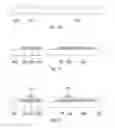
S101: refer now to FIG. 1a, providing a substrate 100; and using a first mask pattern to form a semiconductor pattern on the substrate 100, which includes an active area 101 of a first thin film transistor and an active area 102 of a second thin film transistor in each driving unit.
Specifically, by a method of physical vapor deposition (PVD), a layer of a-Si (amorphous silicon) film is deposited on the substrate 100, and a wet etching method is used to process the a-Si film by the first mask pattern, so as to form the active area 101 of the first thin film transistor and the active area 102 of the second thin film transistor.
S102: refer now to FIG. 1b, based on the above pattern, using a second mask pattern to form an electro-conductive channel of the first thin film transistor and an electro-conductive channel of the second thin film transistor on the substrate 100; and using an ion-injection method to form a channel doping area 103 of the first thin film transistor, a channel doping area 104 of the second thin film transistor, a source electrode doping area 105 and a drain electrode doping area 106 beside two sides of the channel doping area 103 of the first thin film transistor, and a source electrode doping area 107 and a drain electrode doping area 108 beside two sides of the channel doping area 104 of the second thin film transistor.
S103: refer now to FIG. 1c, based on the above pattern, forming a pattern of an insulation layer 109.
Specifically, by a method of chemical vapor deposition (CVD), the insulation layer 109 is deposited on the substrate 100 and the semiconductor pattern.
S104: refer now to FIG. 1c, based on the above pattern, using a third mask pattern to form a pattern of a first metal layer, which includes a gate electrode 110 of the first thin film transistor and a gate electrode 111 of the second thin film transistor.
Specifically, by a method of PVD, the first metal layer is deposited on the insulation layer 109, and a wet etching method is used to process the first metal layer by the third mask pattern, so as to form the gate electrode 110 of the first thin film transistor and the gate electrode 111 of the second thin film transistor.
S105: refer now to FIG. 1d, based on the above pattern, forming a pattern of an interlayer 112; and using an fourth mask pattern to form a via 113 which is in the first thin film transistor and passes through the insulation layer 109 and the interlayer, and a via 114 which is in the second thin film transistor and passes through the insulation layer 109 and the interlayer.
Specifically, a wet etching method is used to process the interlayer 112 and the insulation layer 109 by the fourth mask pattern, so as to form vias passing through the insulation layer 109 and the interlayer, which includes a via configured to connect the source electrode and the source electrode doping area 105 of the first thin film transistor; a via configured to connect the drain electrode and the drain electrode doping area 106; a via configured to connect the drain electrode and the gate electrode 111 of the second thin film transistor; a via configured to connect the source electrode and the source electrode doping area 107 of the second thin film transistor; and a via configured to connect the drain electrode and the drain electrode doping area 108 of the second thin film transistor.
S106: refer now to FIG. 1e, based on the above pattern, using a fifth mask pattern to form a pattern of a second metal layer, which includes a source electrode 115 and a drain electrode 116 of the first thin film transistor, and a source electrode and a drain electrode 118 of the second thin film transistor, and a data line and a pixel electrode.
Specifically, the source electrode of the second thin film transistor is positioned in the same layer of the drain electrode 116 of the first thin film transistor, and are positioned behind the drain electrode 116 of the first thin film transistor, so that the source electrode of the second thin film transistor is covered, and is not shown in the figures.
Finally, refer now to FIG. 1f, based on the above pattern, depositing a PV protecting layer 119, and etching and removing the PV protecting layer 119 on the surface of the pixel electrode, so as to finish the manufacture of the array substrate.
Specifically, before manufacturing semiconductor layers, a buffer layer is formed on the substrate.
Specifically, because the source electrode and drain electrode of the first thin film transistor, the source electrode and drain electrode of the second thin film transistor, and the pixel electrode are manufactured in the same layer, they are all selected from a material of a graphene film with high electric conductivity and high transparency.
According to the above-mentioned method, an array substrate of an OLED display device is obtained. refer now to FIG. 2, the array substrate of the OLED display device of the embodiment includes:
A substrate 201; an active layer formed on the substrate 201 and including a channel doping area 202, a source electrode doping area 203, and a drain electrode doping area 204 of a first thin film transistor T1; and a channel doping area 205, a source electrode doping area 206, and a drain electrode doping area 207 of a second thin film transistor T2; a gate electrode insulation layer 208 formed above the substrate 201; a first metal layer formed above the substrate 201 and including a gate electrode 211 of the first thin film transistor T1 and a gate electrode 212 of the second thin film transistor T2; an interlayer 213 formed above the substrate 201; vias passing through the interlayer 213 and the gate electrode insulation layer 208; and a second metal layer formed above the substrate 201 and including a source electrode 214 and a drain electrode 215 of the first thin film transistor T1; a source electrode and a drain electrode 216 of the second thin film transistor T2; and a data line and a pixel electrode; wherein, the source electrode 214 of the first thin film transistor T1 is connected with the data line; the drain electrode 215 of the first thin film transistor T1 is connected with the gate electrode 212 of the second thin film transistor T2; and the drain electrode 216 of the second thin film transistor T2 is connected with the pixel electrode.
After the above-mentioned steps being finished, a hole-inject layer, a hole-transport layer, an emitting layer, an electron-transport layer, and an anode electrode are manufactured on the pixel electrode of the array substrate in order, so as to obtain the OLED display device.
A drive unit of the OLED display device is composed of two of the thin film transistors (TFT) and one storage capacitor Cst, wherein the gate electrode of the first thin film transistor T1 inputs a scan signal Vgate; the source electrode of the first thin film transistor T1 inputs a data signal Vdata; the drain electrode of the first thin film transistor T1 is connected to the gate electrode of the second thin film transistor T2; the source electrode of the second thin film transistor T2 is connected to a digital power Vdd; the drain electrode of the second thin film transistor T2 is connected to a digital ground Vss; the storage capacitor Cst is disposed between the gate electrode and source electrode of the second thin film transistor T2; and an light-emitting diode is series connected between the drain electrode of the second thin film transistor T2 and the digital ground Vss.
Preferably, a protecting layer 217 is formed above the substrate 201, and a portion of the protecting layer 217 which is on the surface of the pixel electrode is etched.
Preferably, the hole-inject layer and the hole-transport layer are formed above the substrate 201.
Preferably, the second metal layer is selected from a material of a graphene film.
Preferably, a buffer layer is formed between the active layer and the substrate 201.
The advantageous effects of the present invention are: compared with a manufacturing method of a conventional array substrate, in the manufacturing method of the present invention, the data line, the source electrode, the drain electrode, and the pixel electrode can be obtain by the same mask, so that the required masks for processing the different electrodes are saved, and the required masks for forming the vias to connect with the electrodes in the different layers are also reduced. Thus, the exposing processes is reduced; the process complexity is lowered; the material is saved; the processing time is shortened; and the processing cost is simultaneously decreased.
The present invention has been described with preferred embodiments thereof and it is understood that many changes and modifications to the described embodiment can be carried out without departing from the scope and the spirit of the invention that is intended to be limited only by the appended claims.
Claims
What is claimed is:1. A manufacturing method of an array substrate of an OLED display device, comprising steps of:
providing a substrate;
using a first mask pattern to form a semiconductor pattern on the substrate, which includes active areas of a first thin film transistor and a second thin film transistor in each driving unit;
based on the above pattern, using a second mask pattern to form an electro-conductive channel of the first thin film transistor and an electro-conductive channel of the second thin film transistor on the substrate; and using an ion-injection method to form a channel doping area, and form a source electrode doping area and a drain electrode doping area beside two sides of each of the channel doping areas;
based on the above pattern, forming a pattern of an insulation layer;
based on the above pattern, using a third mask pattern to form a pattern of a first metal layer, which includes a gate electrode of the first thin film transistor and a gate electrode of the second thin film transistor;
based on the above pattern, forming a pattern of an interlayer; and using an fourth mask pattern to form a via which is in the first thin film transistor and passes through the insulation layer and the interlayer, and a via which is in the second thin film transistor and passes through the insulation layer and the interlayer;
based on the above pattern, using a fifth mask pattern to form a pattern of a second metal layer, which includes a source electrode and a drain electrode of the first thin film transistor, a source electrode and a drain electrode of the second thin film transistor, and a data line and a pixel electrode; and
based on the above pattern, forming a protecting layer, and etching to remove the protecting layer on the surface of the pixel electrode through a sixth mask pattern.
2. The manufacturing method according to claim 1, wherein based on the above pattern, forming a hole-inject layer and a hole-transport layer.
3. The manufacturing method according to claim 1, wherein the second metal layer is selected from a material of a graphene film.
4. The manufacturing method according to claim 1, wherein before forming the semiconductor pattern, a buffer layer is formed on the substrate.
5. The manufacturing method according to claim 1, wherein the step of forming a semiconductor pattern on the substrate comprises:
using a method of physical vapor deposition to deposit a layer of a-Si film on the substrate, and then using a wet etching method to process the a-Si film by the first mask pattern, so as to form the active areas of the first thin film transistor and the second thin film transistor.
6. A manufacturing method of an array substrate of an OLED display device, comprising steps of:
providing a substrate;
using a first mask pattern to form a semiconductor pattern on the substrate, which includes active areas of a first thin film transistor and a second thin film transistor in each driving unit;
based on the above pattern, using a second mask pattern to form an electro-conductive channel of the first thin film transistor and an electro-conductive channel of the second thin film transistor on the substrate; and using an ion-injection method to form a channel doping area, and form a source electrode doping area and a drain electrode doping area beside two sides of each of the channel doping areas;
based on the above pattern, forming a pattern of an insulation layer;
based on the above pattern, using a third mask pattern to form a pattern of a first metal layer, which includes a gate electrode of the first thin film transistor and a gate electrode of the second thin film transistor;
based on the above pattern, forming a pattern of an interlayer; and using an fourth mask pattern to form a via which is in the first thin film transistor and passes through the insulation layer and the interlayer, and a via which is in the second thin film transistor and passes through the insulation layer and the interlayer; and
based on the above pattern, using a fifth mask pattern to form a pattern of a second metal layer, which includes a source electrode and a drain electrode of the first thin film transistor, a source electrode and a drain electrode of the second thin film transistor, and a data line and a pixel electrode.
7. The manufacturing method according to claim 6, wherein based on the above pattern, forming a hole-inject layer and a hole-transport layer.
8. The manufacturing method according to claim 6, wherein the second metal layer is selected from a material of a graphene film.
9. The manufacturing method according to claim 6, wherein before forming the semiconductor pattern, a buffer layer is formed on the substrate.
10. The manufacturing method according to claim 6, wherein the step of forming a semiconductor pattern on the substrate comprises:
using a method of physical vapor deposition to deposit a layer of a-Si film on the substrate, and then using a wet etching method to process the a-Si film by the first mask pattern, so as to form the active areas of the first thin film transistor and the second thin film transistor.
11. An array substrate of an OLED display device, comprising:
a substrate;
an active layer formed on the substrate and including: a channel doping area, a source electrode doping area and a drain electrode doping area of a first thin film transistor; and a channel doping area, a source electrode doping area and a drain electrode doping area of a second thin film transistor;
a gate electrode insulation layer formed above the substrate;
a first metal layer formed above the substrate and including a gate electrode of the first thin film transistor and a gate electrode of the second thin film transistor;
an interlayer formed above the substrate;
vias passing through the interlayer and the gate electrode insulation layer; and
a second metal layer formed above the substrate and including: a source electrode and a drain electrode of the first thin film transistor; a source electrode and a drain electrode of the second thin film transistor; and a data line and a pixel electrode;
wherein the source electrode of the first thin film transistor is connected with the data line; the drain electrode of the first thin film transistor is connected with the gate electrode of the second thin film transistor; and
the drain electrode of the second thin film transistor is connected with the pixel electrode.
12. The array substrate according to claim 11, wherein a protecting layer is formed above the substrate, and a portion of the protecting layer which is on the surface of the pixel electrode is etched.
13. The array substrate according to claim 11, wherein a hole-inject layer and a hole-transport layer are formed above the substrate.
14. The array substrate according to claim 11, wherein the second metal layer is selected from a material of a graphene film.
15. The array substrate according to claim 11, wherein a buffer layer is formed between the active layer and the substrate.
Images & Drawings included:


Sources:
- United States Patent and Trademark Office - verify current appl. status at the USPTO↗
Similar patent applications:
- » 20140091291
Array substrate and manufacturing method thereof, OLED display device - » 20190363155
Wiring structure and manufacture method thereof, OLED array substrate and display device - » 20140159010
Array substrate, manufacturing method thereof and OLED display device - » 20190013339
Organic light-emitting diode (OLED) array substrate and manufacturing method thereof and display device - » 20210327965
OLED array substrate, manufacturing method thereof and touch display device - » 20160254494
OLED array substrate, manufacturing method thereof, display panel and display device - » 20170329443
OLED array substrate, manufacturing method thereof and touch display device - » 20190131358
OLED array substrate and manufacturing method thereof, and display device - » 20210265439
PIXEL COMPENSATION CIRCUIT AND MANUFACTURING METHOD THEREOF, OLED ARRAY SUBSTRATE AND MANUFACTURING METHOD THEREOF, AND DISPLAY DEVICE - » 20190027702
Composite transparent electrode, OLED and method for manufacturing thereof, array substrate and display device
Recent applications in this class:
- » 20240237401 2024-07-11
DISPLAY PANEL, METHOD OF FABRICATING SAME AND DISPLAY DEVICE - » 20240237400 2024-07-11
DISPLAY PANEL AND MANUFACTURING METHOD THEREOF - » 20240215312 2024-06-27
DISPLAY PANEL AND DISPLAY DEVICE - » 20240138186 2024-04-25
DISPLAY PANEL, METHOD OF FABRICATING SAME AND DISPLAY DEVICE - » 20240138185 2024-04-25
DISPLAY PANEL AND MANUFACTURING METHOD THEREOF - » 20230380217 2023-11-23
DISPLAY PANEL - » 20230371308 2023-11-16
DISPLAY APPARATUS - » 20230337468 2023-10-19
DISPLAY DEVICE - » 20230309342 2023-09-28
Display panel, pixel driving circuits, and display device - » 20230292550 2023-09-14
DISPLAY DEVICE AND METHOD OF FABRICATING THE SAME
Recent applications for this Assignee:
- » 20220052204 2022-02-17
Amorphous silicon thin film transistor and method for manufacturing the same - » 20210405424 2021-12-30
Array substrate - » 20210358953 2021-11-18
Pixel structure, array substrate, and display device - » 20210336040 2021-10-28
Manufacturing method of TFT substrate - » 20210335832 2021-10-28
Thin film transistor (TFT) array substrate and display panel - » 20210191204 2021-06-24
Pixel structure and display panel containing same - » 20210090528 2021-03-25
Display driving system - » 20210083229 2021-03-18
OLED display panel and manufacturing method thereof - » 20210083010 2021-03-18
Color filter substrate having a filter layer disposed on quantum dot layer - » 20210082358 2021-03-18
White balance method and device for LCD panel