Guard rings for cascode gallium nitride devices
US20180240900A1
2018-08-23
15/955,555
2018-04-17
✅ Patent granted
US 10,312,359 B2
2019-06-04
-
-
Anthony Ho
IPTechLaw
2038-04-17
Abstract:
Implementations of semiconductor devices may include: a plurality of drain fingers and a plurality of source fingers interdigitated with one another; at least one gate; and at gate bus formed to completely surround the plurality of drain fingers and the plurality of source fingers; wherein the gate bus is mechanically and electrically coupled to the at least one gate.
Inventors:
- CHUN-LI LIU 42 🇺🇸 SCOTTSDALE, AZ, United States
- Ali SALIH 75 🇺🇸 Mesa, AZ, United States
- Woochul JEON 22 🇺🇸 Phoenix, AZ, United States
Assignee:
- SEMICONDUCTOR COMPONENTS INDUSTRIES, LLC 3,597 🇺🇸 Phoenix, AZ, United States
Applicant:
Interested in similar patents?
Get notified when new applications in this technology area are published.
Classification:
H01L29/2003 » CPC further
Semiconductor devices adapted for rectifying, amplifying, oscillating or switching, or capacitors or resistors with at least one potential-jump barrier or surface barrier, e.g. PN junction depletion layer or carrier concentration layer; Details of semiconductor bodies or of electrodes thereof; Multistep manufacturing processes therefor; Semiconductor bodies ; Multistep manufacturing processes therefor characterised by the materials of which they are formed including, apart from doping materials or other impurities, only AB compounds Nitride compounds
H01L23/495 IPC
Details of semiconductor or other solid state devices; Arrangements for conducting electric current to or from the solid state body in operation, e.g. leads, terminal arrangements ; Selection of materials therefor consisting of soldered constructions Lead-frames or other flat leads
H01L23/49537 » CPC further
Details of semiconductor or other solid state devices; Arrangements for conducting electric current to or from the solid state body in operation, e.g. leads, terminal arrangements ; Selection of materials therefor consisting of soldered constructions; Lead-frames or other flat leads Plurality of lead frames mounted in one device
H01L23/585 » CPC further
Details of semiconductor or other solid state devices; Structural electrical arrangements for semiconductor devices not otherwise provided for, e.g. in combination with batteries comprising conductive layers or plates or strips or rods or rings
H01L27/0883 » CPC further
Devices consisting of a plurality of semiconductor or other solid-state components formed in or on a common substrate including semiconductor components specially adapted for rectifying, oscillating, amplifying or switching and having at least one potential-jump barrier or surface barrier; including integrated passive circuit elements with at least one potential-jump barrier or surface barrier the substrate being a semiconductor body including only semiconductor components of a single kind including field-effect components only the components being field-effect transistors with insulated gate Combination of depletion and enhancement field effect transistors
H01L29/20 IPC
Semiconductor devices adapted for rectifying, amplifying, oscillating or switching, or capacitors or resistors with at least one potential-jump barrier or surface barrier, e.g. PN junction depletion layer or carrier concentration layer; Details of semiconductor bodies or of electrodes thereof; Multistep manufacturing processes therefor; Semiconductor bodies ; Multistep manufacturing processes therefor characterised by the materials of which they are formed including, apart from doping materials or other impurities, only AB compounds
H01L29/402 » CPC further
Semiconductor devices adapted for rectifying, amplifying, oscillating or switching, or capacitors or resistors with at least one potential-jump barrier or surface barrier, e.g. PN junction depletion layer or carrier concentration layer; Details of semiconductor bodies or of electrodes thereof; Multistep manufacturing processes therefor; Electrodes ; Multistep manufacturing processes therefor Field plates
H01L29/41758 » CPC further
Semiconductor devices adapted for rectifying, amplifying, oscillating or switching, or capacitors or resistors with at least one potential-jump barrier or surface barrier, e.g. PN junction depletion layer or carrier concentration layer; Details of semiconductor bodies or of electrodes thereof; Multistep manufacturing processes therefor; Electrodes ; Multistep manufacturing processes therefor characterised by their shape, relative sizes or dispositions carrying the current to be rectified, amplified or switched; Source or drain electrodes for field effect devices for lateral devices with structured layout for source or drain region, i.e. the source or drain region having cellular, interdigitated or ring structure or being curved or angular
H01L29/1066 » CPC further
Semiconductor devices adapted for rectifying, amplifying, oscillating or switching, or capacitors or resistors with at least one potential-jump barrier or surface barrier, e.g. PN junction depletion layer or carrier concentration layer; Details of semiconductor bodies or of electrodes thereof; Multistep manufacturing processes therefor; Semiconductor bodies ; Multistep manufacturing processes therefor characterised by their shape; characterised by the shapes, relative sizes, or dispositions of the semiconductor regions ; characterised by the concentration or distribution of impurities within semiconductor regions with semiconductor regions connected to an electrode not carrying current to be rectified, amplified or switched and such electrode being part of a semiconductor device which comprises three or more electrodes Gate region of field-effect devices with PN junction gate
H01L27/088 IPC
Devices consisting of a plurality of semiconductor or other solid-state components formed in or on a common substrate including semiconductor components specially adapted for rectifying, oscillating, amplifying or switching and having at least one potential-jump barrier or surface barrier; including integrated passive circuit elements with at least one potential-jump barrier or surface barrier the substrate being a semiconductor body including only semiconductor components of a single kind including field-effect components only the components being field-effect transistors with insulated gate
H01L29/06 IPC
Semiconductor devices adapted for rectifying, amplifying, oscillating or switching, or capacitors or resistors with at least one potential-jump barrier or surface barrier, e.g. PN junction depletion layer or carrier concentration layer; Details of semiconductor bodies or of electrodes thereof; Multistep manufacturing processes therefor; Semiconductor bodies ; Multistep manufacturing processes therefor characterised by their shape; characterised by the shapes, relative sizes, or dispositions of the semiconductor regions ; characterised by the concentration or distribution of impurities within semiconductor regions
H01L29/16 » CPC further
Semiconductor devices adapted for rectifying, amplifying, oscillating or switching, or capacitors or resistors with at least one potential-jump barrier or surface barrier, e.g. PN junction depletion layer or carrier concentration layer; Details of semiconductor bodies or of electrodes thereof; Multistep manufacturing processes therefor; Semiconductor bodies ; Multistep manufacturing processes therefor characterised by the materials of which they are formed including, apart from doping materials or other impurities, only elements of Group IV of the Periodic System
H01L29/40 IPC
Semiconductor devices adapted for rectifying, amplifying, oscillating or switching, or capacitors or resistors with at least one potential-jump barrier or surface barrier, e.g. PN junction depletion layer or carrier concentration layer; Details of semiconductor bodies or of electrodes thereof; Multistep manufacturing processes therefor Electrodes ; Multistep manufacturing processes therefor
H01L29/417 IPC
Semiconductor devices adapted for rectifying, amplifying, oscillating or switching, or capacitors or resistors with at least one potential-jump barrier or surface barrier, e.g. PN junction depletion layer or carrier concentration layer; Details of semiconductor bodies or of electrodes thereof; Multistep manufacturing processes therefor; Electrodes ; Multistep manufacturing processes therefor characterised by their shape, relative sizes or dispositions carrying the current to be rectified, amplified or switched
H01L23/58 IPC
Details of semiconductor or other solid state devices Structural electrical arrangements for semiconductor devices not otherwise provided for, e.g. in combination with batteries
H01L29/10 IPC
Semiconductor devices adapted for rectifying, amplifying, oscillating or switching, or capacitors or resistors with at least one potential-jump barrier or surface barrier, e.g. PN junction depletion layer or carrier concentration layer; Details of semiconductor bodies or of electrodes thereof; Multistep manufacturing processes therefor; Semiconductor bodies ; Multistep manufacturing processes therefor characterised by their shape; characterised by the shapes, relative sizes, or dispositions of the semiconductor regions ; characterised by the concentration or distribution of impurities within semiconductor regions with semiconductor regions connected to an electrode not carrying current to be rectified, amplified or switched and such electrode being part of a semiconductor device which comprises three or more electrodes
H01L29/42316 » CPC further
Semiconductor devices adapted for rectifying, amplifying, oscillating or switching, or capacitors or resistors with at least one potential-jump barrier or surface barrier, e.g. PN junction depletion layer or carrier concentration layer; Details of semiconductor bodies or of electrodes thereof; Multistep manufacturing processes therefor; Electrodes ; Multistep manufacturing processes therefor characterised by their shape, relative sizes or dispositions not carrying the current to be rectified, amplified or switched; Gate electrodes for field effect devices for field-effect transistors
H01L29/778 » CPC main
Semiconductor devices adapted for rectifying, amplifying, oscillating or switching, or capacitors or resistors with at least one potential-jump barrier or surface barrier, e.g. PN junction depletion layer or carrier concentration layer; Details of semiconductor bodies or of electrodes thereof; Multistep manufacturing processes therefor; Types of semiconductor device ; Multistep manufacturing processes therefor controllable by only the electric current supplied, or only the electric potential applied, to an electrode which does not carry the current to be rectified, amplified or switched; Unipolar devices, e.g. field effect transistors; Field effect transistors with two-dimensional charge carrier gas channel, e.g. HEMT ; with two-dimensional charge-carrier layer formed at a heterojunction interface
H01L23/4952 » CPC further
Details of semiconductor or other solid state devices; Arrangements for conducting electric current to or from the solid state body in operation, e.g. leads, terminal arrangements ; Selection of materials therefor consisting of soldered constructions; Lead-frames or other flat leads; Additional leads the additional leads being a bump or a wire
H01L29/423 IPC
Semiconductor devices adapted for rectifying, amplifying, oscillating or switching, or capacitors or resistors with at least one potential-jump barrier or surface barrier, e.g. PN junction depletion layer or carrier concentration layer; Details of semiconductor bodies or of electrodes thereof; Multistep manufacturing processes therefor; Electrodes ; Multistep manufacturing processes therefor characterised by their shape, relative sizes or dispositions not carrying the current to be rectified, amplified or switched
Description
CROSS REFERENCE TO RELATED APPLICATIONS
This application is a divisional application of the earlier U.S. Utility Patent Application to Woochul Jeon et al entitled “Guard Rings For Cascode Gallium Nitride Devices,” application serial number 15/208,466, filed Jul. 12, 2016, now pending, the disclosure of which is hereby incorporated entirely herein by reference.
BACKGROUND
1. Technical Field
Aspects of this document relate generally to guard rings to protect semiconductor devices. More specific implementations involve using guard rings in cascode devices.
2. Background
Gallium nitride (GaN) devices are used in high power/high frequency applications. These devices include source, drain, and gate regions where the source and drain regions are often arranged in an interdigitated fashion.
SUMMARY
Implementations of semiconductor devices may include: a plurality of drain fingers and a plurality of source fingers interdigitated with one another; at least one gate; and at gate bus formed to completely surround the plurality of drain fingers and the plurality of source fingers; wherein the gate bus is mechanically and electrically coupled to the at least one gate.
Implementations of semiconductor devices may include: a depletion mode (D-mode) transistor having one or more source fingers, one or more drain fingers and one or more gates; and a gate bus surrounding the one or more source fingers and the one or more drain fingers of the D-mode transistor; wherein the gate bus couples with the one or more gates of the D-mode transistor; wherein the gate bus is a first guard ring of the D-mode transistor.
Implementations of semiconductor devices may include one, all, or any of the following:
The D-mode transistor may be a gallium nitride (GaN) high electron mobility transistor (HEMT).
The gate bus may be formed from one selected from the group of an ohmic metal, a gate metal, and a field plate.
A channel under the first guard ring may be depleted during one of operation or non-operation of the device.
A channel under the first guard ring may be active during operation of the device.
The semiconductor device further includes at least one additional guard ring surrounding an outer perimeter of the first guard ring.
A channel between the first guard ring and the at least one additional guard ring may be active during operation of the device.
A second guard ring may be coupled to one of a group comprising the gate, the source and a substrate of the device.
A second guard ring may be floating relative to the drain fingers and the source fingers.
Implementations of semiconductor devices may include: a depletion mode (D-mode) transistor having one or more source fingers, one or more drain fingers and one or more gates; an enhanced mode (E-mode) transistor having one or more source pads, one or more drain pads and one or more gate pads; and a gate bus formed as a guard ring of the D-mode transistor; wherein the one or more gate pads of the D-mode transistor couple with the source pads of the E-mode transistor and an electrical ground.
Implementations of semiconductor devices may include one, all, or any of the following:
The D-mode transistor may be a gallium nitride (GaN) high electron mobility transistor (HEMT).
The E-mode transistor is a silicon (Si) field effect transistor (FET).
The semiconductor device further including a second guard ring surrounding an outer perimeter of the first guard ring.
The D-mode transistor is coupled to a first conductive lead frame and the E-mode transistor is coupled to a second conductive lead frame.
The semiconductor device further including a pin out from each of the drain of the D-mode transistor and the gate and the source of the E-mode transistor.
The source of the D-mode transistor may be coupled to the drain of the E-mode transistor.
The source of the D-mode transistor and the drain of the E-mode are coupled together through a wire bond.
The foregoing and other aspects, features, and advantages will be apparent to those artisans of ordinary skill in the art from the DESCRIPTION and DRAWINGS, and from the CLAIMS.
BRIEF DESCRIPTION OF THE DRAWINGS
Implementations will hereinafter be described in conjunction with the appended drawings, where like designations denote like elements, and:
FIG. 1 is a cross-sectional view of a guard ring structure;
FIG. 2 is top view of another guard ring structure;
FIG. 3 is a top view of an implementation of a guard ring structure;
FIG. 4A is a top view of another implementation of a guard ring structure;
FIG. 4B is an enlarged view of a gate pad from FIG. 4A;
FIG. 5A is a top view of another implementation of a guard ring structure;
FIG. 5B is an enlarged view of a corner from the device in FIG. 5A;
FIG. 6 is a view an implementation of a guard ring protecting a device;
FIG. 7 is a top view of a cascode device using an implementation of a guard ring structure.
DESCRIPTION
This disclosure, its aspects and implementations, are not limited to the specific components, assembly procedures or method elements disclosed herein. Many additional components, assembly procedures and/or method elements known in the art consistent with the intended gallium nitride semiconductor device structure will become apparent for use with particular implementations from this disclosure. Accordingly, for example, although particular implementations are disclosed, such implementations and implementing components may comprise any shape, size, style, type, model, version, measurement, concentration, material, quantity, method element, step, and/or the like as is known in the art for such gallium nitride semiconductor device structures and implementing components and methods, consistent with the intended operation and methods.
Examples of semiconductor devices having guard rings may be in found in U.S. Patent Publication No. 2013/0126888 to Kizilyalli et al., entitled “Edge Termination by Ion Implantation in GAN,” published May 23, 2013, and filed Nov. 21, 2011 and U.S. Pat. No. 9,165,999 to Kentaro Ikeda, entitled “Nitride Semiconductor Device,” issued Oct. 20, 2015 and filed Mar. 15, 2013, the disclosures of each which are hereby incorporated entirely herein by reference.
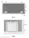
Referring to FIG. 1, a semiconductor device 2 having a guard ring structure is illustrated. This device has an elevated field region. The gate 4 structure and the source 6 structure of this device are located on positively and negatively doped regions of the device 2. The guard ring 8 is formed through ion implantation at the edge of the device to form a resistive layer.
Referring to FIG. 2, another semiconductor device 9 having a guard ring structure is illustrated. This guard ring structure 10 is formed by a layer of isolation between the device region 12 and the guard ring 14, isolating the device from the two dimensional electron gas (2DEG).
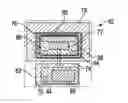
Referring now to FIG. 3, an implementation of a semiconductor device 16 having a guard ring structure is illustrated. A first guard ring 18 is formed around a device region 20. The device region 20 includes a plurality of drain fingers 22 and a plurality of source fingers 24 interdigitated with one another. In this implementation there are two gates 26, however, in other implementations, a single gate may be used. A gate bus 28 is mechanically and electrically coupled to the gates 26 and functions as a first guard ring 18. The first guard ring 18 completely surrounds the device region/die 20. The first guard ring 18 can be coupled to the substrate through ohmic/electrical contacts. The channel under the first guard ring 18 may be either depleted or an active 2DEG during the operation of the device. A second guard ring 30 is also illustrated. Multiple guard rings may be used in implementations of semiconductor devices having guard rings as described here. By non-limiting example, additional guard rings may be connected to the gate, the source, or the substrate of the device. The guard rings may also be floating guard rings, floating relative to the drain, source and gate of the device. The channel present between the guard rings 18 and 30 may be either depleted or an active 2DEG. The device may be a high electron mobility transistor (HEMT) formed from gallium nitride (GaN) or any other suitable semiconductor known in the art.
Referring now to FIG. 4A, another implementation of a semiconductor device 34 having guard rings 36 is illustrated. The device may be a depletion mode (D-mode) transistor 38 having one or more source fingers 40, one or more drain fingers 42 and one or more gates 44. A gate bus 36 surrounds the one or more source fingers and the one or more drain fingers. The gate bus 36 couples with the one or more gates 44 of the D-mode transistor. An enlarged view of the gate 44 and guard ring 36 is illustrated in FIG. 4B. The guard ring 36 is grounded through the gate 44 which may reduce the capacitance between the source and the substrate of the device.
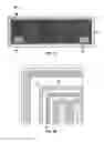
Referring now to FIG. 5A, an implementation of a semiconductor device 46 having multiple guard rings is illustrated. An enlarged view of the corner of the device is illustrated in FIG. 5B. The gate bus acts as the first guard ring 48 and is coupled to the gates 50 of the device 46 as previously described in other implementations. In addition, a second 52 and third 54 guard ring are illustrated. The second 52 and third guard ring 54 may be coupled to the source and/or the substrate of the device. The layers used for the guard rings may be any suitable metal known in the art such as metals used for ohmic, gate, or field plate applications. Referring to FIG. 6, multiple guard rings may physically protect the device 56 as well. The gallium nitride epitaxial layer 58 can easily be damaged during sawing. Here, the second guard ring 60 blocked the transfer of a crack or chipping defect 59, occurring during sawing, into the device.
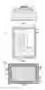
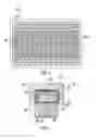
Referring now to FIG. 7, an implementation of a cascode device 62 having a gate 64 connected guard ring 66 is illustrated. A depletion mode (D-mode) transistor 68 is surrounded by a first guard ring 66 coupled to the gate 64. The D-mode transistor may be a GaN HEMT. A second guard ring 76 is surrounding an outer perimeter of the first guard ring 66. The D-mode transistor is coupled to a conductive lead frame 78 having leads coming out from the drain 80. More specifically, the lead frame 78 is connected to the gate pad 64, the drain pad 80 has a separate pin-out, and the gate and source of the silicon metal oxide semiconductor field effect transistor (Si-MOSFET) 86 are electrically connected. The D-mode transistor 68 is coupled to an enhancement mode (E-mode) transistor 70. The transistors may be coupled through wire bonds. The E-mode transistor may be a silicon (Si) field effect transistor (FET). The source 72 of the D-mode transistor is coupled to the substrate 74 of the E-mode transistor. The E-mode transistor 70 is coupled to a second conductive lead frame 82. The gate 84 and the source 86 of the E-mode transistor may have lead outs to connect to other devices. During operation of this implementation of a cascode device, the gate 64 of D-mode transistor 68 is connected to the ground. Having the gate 64 connected to the guard ring 66 may help to keep the potential at the guard ring constant (0V) and may effectively protect the device 62. The built-up charges between the source and the substrate can be significantly reduced.
Implementations of GaN devices like those disclosed herein may be manufactured by those of ordinary skill in the art using a wide variety of processing methods and techniques using the principles disclosed herein.
In places where the description above refers to particular implementations of gallium nitride semiconductor devices and implementing components, sub-components, methods and sub-methods, it should be readily apparent that a number of modifications may be made without departing from the spirit thereof and that these implementations, implementing components, sub-components, methods and sub-methods may be applied to other gallium nitride semiconductor devices.
Claims
What is claimed is:1. A semiconductor device comprising:
a depletion mode (D-mode) transistor comprising one or more source fingers, one or more drain fingers and one or more gates;
an enhanced mode (E-mode) transistor comprising one or more source pads, one or more drain pads and one or more gate pads; and
a gate bus formed as a guard ring of the D-mode transistor;
wherein the gate bus is coupled with one or more gate pads of the D-mode transistor; and
wherein the one or more gate pads of the D-mode transistor couple with the source pads of the E-mode transistor and an electrical ground.
2. The semiconductor device of claim 1, wherein the D-mode transistor is a gallium nitride (GaN) high electron mobility transistor (HEMT).
3. The semiconductor device of claim 1, wherein the E-mode transistor is a silicon (Si) field effect transistor (FET).
4. The semiconductor device of claim 1, further comprising a second guard ring surrounding an outer perimeter of the first guard ring.
5. The semiconductor device of claim 1, wherein the D-mode transistor is coupled to a first conductive lead frame and the E-mode transistor is coupled to a second conductive lead frame.
6. The semiconductor device of claim 1, further comprising a pin out from each of the drain of the D-mode transistor and the gate and the source of the E-mode transistor.
7. The semiconductor device of claim 1, wherein the source of the D-mode transistor is coupled to the drain of the E-mode transistor.
8. The semiconductor device of claim 1, wherein the source of the D-mode transistor and the drain of the E-mode transistor are coupled together through a wire bond.
9. A semiconductor device comprising:
a depletion mode (D-mode) transistor comprising one or more source fingers, one or more drain fingers and one or more gates;
an enhanced mode (E-mode) transistor comprising one or more source pads, one or more drain pads and one or more gate pads; and
a gate bus formed as a guard ring of the D-mode transistor;
wherein the gate bus is coupled with one or more gate pads of the D-mode transistor; and
wherein the one or more gate pads of the D-mode transistor couple with the source pads of the E-mode transistor and an electrical ground; and
wherein the source is not grounded.
10. The semiconductor device of claim 9, wherein the D-mode transistor is a gallium nitride (GaN) high electron mobility transistor (HEMT).
11. The semiconductor device of claim 9, wherein the E-mode transistor is a silicon (Si) field effect transistor (FET).
12. The semiconductor device of claim 9, further comprising a second guard ring surrounding an outer perimeter of the first guard ring.
13. The semiconductor device of claim 9, wherein the D-mode transistor is coupled to a first conductive lead frame and the E-mode transistor is coupled to a second conductive lead frame.
14. The semiconductor device of claim 9, further comprising a pin out from each of the drain of the D-mode transistor and the gate and the source of the E-mode transistor.
15. The semiconductor device of claim 9, wherein the source of the D-mode transistor is coupled to the drain of the E-mode transistor.
16. The semiconductor device of claim 9, wherein the source of the D-mode transistor and the drain of the E-mode transistor are coupled together through a wire bond.
17. A semiconductor device comprising:
a depletion mode (D-mode) transistor comprising one or more source fingers, one or more drain fingers and one or more gates;
an enhanced mode (E-mode) transistor comprising one or more source pads, one or more drain pads and one or more gate pads; and
a gate bus formed as a guard ring of the D-mode transistor;
a second guard ring surrounding an outer perimeter of the first guard ring;
wherein the gate bus is coupled with one or more gate pads of the D-mode transistor; and
wherein the one or more gate pads of the D-mode transistor couple with the source pads of the E-mode transistor and an electrical ground.
18. The semiconductor device of claim 17, wherein a channel between the gate bus and the second guard ring is depleted.
19. The semiconductor device of claim 17, wherein a channel between the gate bus and the second guard ring is active.
20. The semiconductor device of claim 17, wherein the D-mode transistor is coupled to a first conductive lead frame and the E-mode transistor is coupled to a second conductive lead frame.
Images & Drawings included:
Sources:
- United States Patent and Trademark Office - verify current appl. status at the USPTO↗
Similar patent applications:
- » 20180019332
Guard rings for cascode gallium nitride devices - » 20190245072
Guard rings for cascode gallium nitride devices
Recent applications in this class:
- » 20250048667 2025-02-06
SEMICONDUCTOR DEVICE WITH GATE ELECTRICAL CONTACT FORMING JUNCTIONS HAVING DIFFERENT ENERGY BARRIER HEIGHTS TO GATE LAYER - » 20240379834 2024-11-14
RECESSED-GATE HIGH-ELECTRON-MOBILITY TRANSISTORS WITH DOPED BARRIERS AND ROUND GATE FOOT CORNERS - » 20240371990 2024-11-07
III-Nitride Vertical Hot Electron Transistor With Polarization Doping And Collimated Injection - » 20240355916 2024-10-24
GAN-BASED HEMT DEVICE, DEVICE EPITAXIAL STRUCTURE, AND PREPARATION METHOD THEREOF - » 20240304711 2024-09-12
HEMT DEVICE HAVING A REDUCED ON-RESISTANCE AND MANUFACTURING PROCESS THEREOF - » 20240304710 2024-09-12
HEMT DEVICE HAVING IMPROVED ON-STATE PERFORMANCE AND MANUFACTURING PROCESS THEREOF - » 20240290875 2024-08-29
HIGH ELECTRON MOBILITY TRANSISTOR AND METHOD FOR FABRICATING THE SAME - » 20240274702 2024-08-15
HEMT TRANSISTOR - » 20240266425 2024-08-08
HEMT TRANSISTOR - » 20240234559 2024-07-11
High electron mobility transistor and method for fabricating the same
Recent applications for this Assignee:
- » 20240348142 2024-10-17
LOW POWER GREEN MODE FOR MULTI-PHASE POWER CONVERTERS - » 20240290757 2024-08-29
SANDWICH PACKAGE FOR MICROELECTRONICS - » 20240290736 2024-08-29
MOLDED THIN SEMICONDUCTOR DIE PACKAGES AND RELATED METHODS - » 20240282668 2024-08-22
PROTECTION DAM FOR A POWER MODULE WITH SPACERS - » 20240275272 2024-08-15
Methods and systems of power-factor-correction converters - » 20240274506 2024-08-15
JET IMPINGEMENT HEATSINK FOR HIGH POWER SEMICONDUCTOR DEVICES - » 20240266264 2024-08-08
SEMICONDUCTOR PACKAGES WITH WETTABLE FLANKS AND RELATED METHODS - » 20240266252 2024-08-08
SINGLE SWITCH DIRECT COOLING ASSEMBLIES AND RELATED METHODS - » 20240259701 2024-08-01
Methods for mitigating lag in image sensor devices - » 20240258181 2024-08-01
Substrates and related methods