Synchronous oscillation circuit
US20180241346A1
2018-08-23
15/439,977
2017-02-23
✅ Patent granted
US 10,333,531 B2
2019-06-25
-
-
Ryan Johnson
Bacon & Thomas, PLLC
2037-09-16
Abstract:
A synchronous oscillation circuit has multiple oscillators, a grounding unit and a common floating grounding unit. Each of the oscillators has a ground terminal. The grounding unit has a first terminal and a second terminal, wherein the second terminal is grounded. The common floating grounding unit is electrically connected between the ground terminals of the oscillators and the first terminal of the grounding unit. The oscillators are grounded through the common floating grounding unit and the grounding unit, so that the oscillators interfere with each other. When the oscillation signals generated by the oscillators reach a steady state, the oscillation frequencies of the oscillators are synchronized.
Assignee:
- NATIONAL CHUNG CHENG UNIVERSITY 49 🇹🇼 CHIAYI COUNTY, Taiwan
Applicant:
Interested in similar patents?
Get notified when new applications in this technology area are published.
Classification:
H03B5/24 » CPC main
Generation of oscillations using amplifier with regenerative feedback from output to input with frequency-determining element comprising resistance and either capacitance or inductance, e.g. phase-shift oscillator active element in amplifier being semiconductor device
H03L7/099 » CPC main
Automatic control of frequency or phase; Synchronisation using a reference signal applied to a frequency- or phase-locked loop; Details of the phase-locked loop concerning mainly the controlled oscillator of the loop
H03B5/1203 » CPC further
Generation of oscillations using amplifier with regenerative feedback from output to input with frequency-determining element comprising lumped inductance and capacitance active element in amplifier being semiconductor device the amplifier being a single transistor
H03B5/362 » CPC further
Generation of oscillations using amplifier with regenerative feedback from output to input with frequency-determining element being electromechanical resonator being a piezo-electric resonator active element in amplifier being semiconductor device the amplifier being a single transistor
H03B2200/001 » CPC further
Indexing scheme relating to details of oscillators covered by; Types of oscillators Hartley oscillator
H03K3/0315 » CPC further
Circuits for generating electric pulses; Monostable, bistable or multistable circuits; Generators characterised by the type of circuit or by the means used for producing pulses by the use of logic circuits, with internal or external positive feedback; Astable circuits Ring oscillators
H03B5/12 IPC
Generation of oscillations using amplifier with regenerative feedback from output to input with frequency-determining element comprising lumped inductance and capacitance active element in amplifier being semiconductor device
H03B27/00 » CPC further
Generation of oscillations providing a plurality of outputs of the same frequency but differing in phase, other than merely two anti-phase outputs
H03B2200/0008 » CPC further
Indexing scheme relating to details of oscillators covered by; Types of oscillators Colpitts oscillator
H03L7/24 » CPC further
Automatic control of frequency or phase; Synchronisation using a reference signal directly applied to the generator
H03B5/36 IPC
Generation of oscillations using amplifier with regenerative feedback from output to input with frequency-determining element being electromechanical resonator being a piezo-electric resonator active element in amplifier being semiconductor device
H03K3/03 IPC
Circuits for generating electric pulses; Monostable, bistable or multistable circuits; Generators characterised by the type of circuit or by the means used for producing pulses by the use of logic circuits, with internal or external positive feedback Astable circuits
G06F1/12 » CPC further
Details not covered by groups - and; Generating or distributing clock signals or signals derived directly therefrom Synchronisation of different clock signals provided by a plurality of clock generators
H03B2200/0074 » CPC further
Indexing scheme relating to details of oscillators covered by; Functional aspects of oscillators Locking of an oscillator by injecting an input signal directly into the oscillator
Description
BACKGROUND OF THE INVENTION
1. Field of the Invention
The present invention relates to a synchronous oscillation circuit, especially a synchronous oscillation circuit synchronizing the oscillation signals generated by multiple oscillators.
2. Description of the Prior Arts
A synchronous oscillation circuit has multiple oscillators for generating oscillating signals. An injection locking technique is generally used to synchronize the oscillating signals generated by the multiple oscillators.
However, the injection locking technique may possibly cause transmission delay for oscillation signals. Such delay problem may not be obvious for oscillation signals. However, for extremely high frequency oscillation signals, i.e. the oscillating frequency is approximately 30-300 GHz, it would be difficult to synchronize the oscillation signals by the injection locking technique.
SUMMARY OF THE INVENTION
The purpose of the present invention is to provide a synchronous oscillation circuit without using the injection locking technique. The synchronous oscillation circuit comprises:
multiple oscillators, each one of the oscillators having a ground terminal;
a grounding unit having a first terminal and a second terminal, wherein the second terminal is grounded; and
a common floating grounding unit electrically connected between the ground terminals of the oscillators and the first terminal of the grounding unit.
According to the present invention, the ground terminals of the oscillators are connected with each other through the common floating grounding unit, so that the oscillators interfere with each other. When the oscillation signals generated by the oscillators reach a steady state, the oscillation frequencies of the oscillators will be synchronized. Compared with the prior art, the oscillation signals can still be successfully synchronized even when wavelengths of the oscillation signals are up to millimeters.
BRIEF DESCRIPTION OF THE DRAWINGS
FIG. 1 is a block circuit diagram of the first preferred embodiment of a synchronous oscillation circuit of the present invention;
FIG. 2 is a circuit diagram of the first preferred embodiment of an oscillator of the synchronous oscillation circuit as shown in FIG. 1;
FIG. 3 is a circuit diagram of the second preferred embodiment of an oscillator of the synchronous oscillation circuit as shown in FIG. 1;
FIG. 4 is a circuit diagram of the third preferred embodiment of an oscillator of the synchronous oscillation circuit as shown in FIG. 1;
FIG. 5 is a circuit diagram of the fourth preferred embodiment of an oscillator of the synchronous oscillation circuit as shown in FIG. 1;
FIG. 6 is a block circuit diagram of the second preferred embodiment of the synchronous oscillation circuit;
FIG. 7 is a circuit diagram of the first preferred embodiment of an oscillator of the synchronous oscillation circuit as shown in FIG. 6;
FIG. 8 is a circuit diagram of the second preferred embodiment of an oscillator of the synchronous oscillation circuit as shown in FIG. 6;
FIG. 9 is a circuit diagram of the third preferred embodiment of an oscillator of the synchronous oscillation circuit as shown in FIG. 6;
FIG. 10 is a signal oscillogram of the oscillation signals generated by two oscillators of an embodiment of the present invention from 0 ns (nanosecond) to 10 ns;
FIG. 11 is a signal oscillogram of the oscillation signals generated by two oscillators of an embodiment of the present invention from 6 ns to 10 ns of as shown in FIG. 10;
FIG. 12 is a signal oscillogram of the oscillation signals generated by two oscillators of an embodiment of the present invention from 96 ns to 100 ns;
FIG. 13 is a signal oscillogram of the oscillation signals generated by two oscillators of another embodiment of the present invention from 0 ns (nanosecond) to 10 ns;
FIG. 14 is a signal oscillogram of the oscillation signals generated by two oscillators of said another embodiment of the present invention from 6 ns to 10 ns of as shown in FIG. 13;
FIG. 15 is a signal oscillogram of the oscillation signals generated by two oscillators of said another embodiment of the present invention from 96 ns to 100 ns;
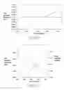
FIG. 16 shows characteristic curves of the grid voltage and the free oscillation frequency of the voltage-controlled oscillator of the present invention;
FIG. 17 shows characteristic curves of the grid voltage, the phase difference and the free oscillation frequency of the voltage-controlled oscillator of the present invention.
DETAILED DESCRIPTION OF THE INVENTION
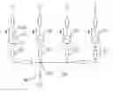
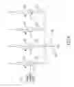
As shown in FIG. 1, a synchronous oscillation circuit comprises multiple oscillators 10, a grounding unit 20 and a common floating grounding unit 30. Please note that the embodiment with four oscillators 10 as shown in FIG. 1 is just taken as an example, not limiting the present invention. Each oscillator 10 has a signal output terminal Vout and a ground terminal G. The signal output terminal Vout outputs an oscillation signal y. The grounding unit 20 has a first terminal and a second terminal, wherein the second terminal is grounded. The common floating grounding unit 30 is electrically connected between the ground terminals G of the oscillators 10 and the first terminal of the grounding unit 20, which means that rather than grounding directly, the ground terminals G of the oscillators 10 are grounded via the common floating grounding unit 30 and the grounding unit 20.
As shown in FIG. 1, the common floating grounding unit 30 comprises a common node 31 and multiple electronic components 32. The common node 31 is a floating common-ground node. The ground terminals G of the oscillators 10 are electrically connected to the common node 31 via the electronic components 32 respectively. The electronic component 32 may be a transmission line, a wire or an RLC circuit composed of a resistor, an inductor and a capacitor. Moreover, the first terminal of the grounding unit 20 is electrically connected to the common node 31 of the common floating grounding unit 30. The grounding unit 20 may be an inductor, an RLC circuit, a transmission line or a wire. Please note that the inductor as shown in FIG. 1 is just taken as an example to illustrate the grounding unit 20, and the grounding unit 20 is not limited to the inductor.
For instance, the oscillator 10 may be, but not limited to, an LC resonant cavity oscillator, a Voltage-Controlled Oscillator (VCO), a Colpitts oscillator, a Ring oscillator, a Hartley oscillator or a transistor-based oscillator. FIG. 2 is a typical circuit of the Colpitts oscillator. The ground terminal G of the Colpitts oscillator is electrically connected to the common node 31 via the electronic component 32 of the common floating grounding unit 30. FIG. 3 is a typical circuit of the Ring oscillator. The ground terminal G of the Ring oscillator is electrically connected to the common node 31 via the electronic component 32 of the common floating grounding unit 30. FIG. 4 is a typical circuit of the Hartley oscillator. The ground terminal G of the Hartley oscillator is electrically connected to the common node 31 via the electronic component 32 of the common floating grounding unit 30. FIG. 5 is a typical circuit of the transistor-based oscillator. The ground terminal G of the transistor-based oscillator is electrically connected to the common node 31 via the electronic component 32 of the common floating grounding unit 30.
Although the oscillators 10 are operated independently, the ground terminals G of the oscillators 10 are all connected together by the common floating grounding unit 30. Hence, the oscillators 10 interfere with each other. When the oscillation signals generated by the oscillators 10 reach the steady state, the oscillation frequency and phase of the oscillation signals will be synchronized.
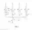
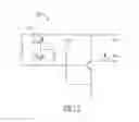
In another embodiment, the phase of the oscillation signal ψ are adjustable, such that there are phase differences among different oscillation signals ψ generated by different oscillators 10. As shown in FIG. 6, each oscillator comprises a phase modulation circuit 11 that modulates the phase of the oscillation signal ψ generated by this oscillator 10. Therefore, the phase modulation circuit 11 is integrated into the oscillator 10 instead of an external phase-shift circuit to achieve the advantages of simplified circuit, saving space and reducing cost. Moreover, any one of the oscillators 10 can be electrically connected to a phase-locked loop (PLL) 12, adapted as a master oscillator to obtain a stable frequency output.
Taking the typical cruciate Colpitts oscillator as shown in FIG. 7 as an example, the Colpitts oscillator comprises a first capacitor C1 and a second capacitor C2. One terminal of the first capacitor C1 and one terminal of the second capacitor C2 are electrically connected to the common node 31 via the electronic component 32 of the common floating grounding unit 30. The first capacitor C1 and the second capacitor C2 are variable capacitors and form the phase modulation circuit 11. Therefore, the phase of the oscillation signal ψ can be modulated by adjusting the capacitance of the first capacitor C1 and the second capacitor C2.
Taking the typical cruciate Hartley oscillator as shown in FIG. 8 as another example, the Hartley oscillator comprises a capacitor C. The capacitor C is a variable capacitor and functions as the phase modulation circuit 11. The phase of the oscillation signal y can be modulated by adjusting the capacitance of the capacitor C.
Taking the typical cruciate transistor-based oscillator as shown in FIG. 9 as another example, the transistor-based oscillator comprises a first capacitor C1 and a second capacitor C2. The common node of the first capacitor C1 and the second capacitor C2 is electrically connected to the signal output terminal Vout of the oscillator. The first capacitor C1 and the second capacitor C2 are variable capacitors and form the phase modulation circuit 11. The phase of the oscillation signal y can be modulated by adjusting the capacitance of the first capacitor C1 and the second capacitor C2.
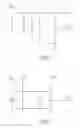
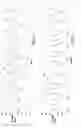
The modulation of the phases of the oscillation signals will be illustrated by the following signal oscillograms. Taking the oscillation signals generated by two oscillators as an example, as shown in FIG. 10 and FIG. 11, one oscillator generates a first oscillation signal ψ1, and the other oscillator generates a second oscillation signal ψ2. The initial values of the natural frequency of the first oscillation signal ψ1 and the second oscillation signal ψ2 are the same, e.g. the initial value is 2.5 GHz. The phase of the second oscillation signal ψ2 lags behind the phase of the first oscillation signal ψ1. By modulating the modulation circuit 11 of either or both of the two oscillators, as shown in FIG. 12, the phases of the first oscillation signal ψ1 and the second oscillation signal ψ2 can be the same in the steady state.
Taking the oscillation signals generated by two oscillators as another example, as shown in FIG. 13 and FIG. 14, one oscillator generates a third oscillation signal ψ3, and the other oscillator generates a fourth oscillation signal ψ4. The initial value of the natural frequency of the third oscillation signal ψ3 is different from the fourth oscillation signal ψ4, e.g. the initial value of the third oscillation signal ψ3 is 2.5 GHz while the initial value of the fourth oscillation signal ψ4 is 2.497 GHz. The phases of the third oscillation signal ψ3 and the fourth oscillation signal ψ4 are the same. Because the two oscillators interfere with each other, the free oscillation frequency can be synchronized by 2.498 GHz in the steady state as shown in FIG. 15. Besides, by modulating the modulation circuit of either or both of the two oscillators, the phase of the third oscillation signal ψ3 can lag behind the fourth oscillation signal ψ4.
The typical Voltage-Controlled Oscillator (VCO) comprises a voltage controlled transistor. The free oscillation frequency of the Voltage-Controlled Oscillator can be modulated by adjusting a gate voltage of the voltage controlled transistor. As shown in FIG. 16, taking a first Voltage-Controlled Oscillator and a second Voltage-Controlled Oscillator as an example, the free oscillation frequency of the oscillation signal, shown by the solid line, generated by the first Voltage-Controlled Oscillator remains at 2.5 GHz. The free oscillation frequency of the oscillation signal, shown by broken lines, generated by the second Voltage-Controlled Oscillator can be modulated by adjusting the gate voltage of the voltage controlled transistor of the second Voltage-Controlled Oscillator. As shown in FIG. 16, the gate voltage of the voltage controlled transistor of the second Voltage-Controlled Oscillator is proportional to the free oscillation frequency of the oscillation signal generated by the second Voltage-Controlled Oscillator.
Besides, as shown in FIG. 17, under the circumstances that the free oscillation frequency of the oscillation signal generated by the first Voltage-Controlled Oscillator is 2.5 GHz and the gate voltage of the voltage controlled transistor of the second Voltage-Controlled Oscillator is proportional to the free oscillation frequency, shown by the broken lines, of the oscillation signal generated by the second Voltage-Controlled Oscillator, there can be a phase difference, shown by the solid line, between the oscillation signals generated by the first Voltage-Controlled Oscillator and the second Voltage-Controlled Oscillator. As the gate voltage of the voltage controlled transistor of the second Voltage-Controlled Oscillator increases, the phase difference is changed from a positive value to a negative value. Therefore, by adjusting the gate voltage of the voltage controlled transistor, an oscillation signal with desirable phase or free oscillation frequency can be generated by the Voltage-Controlled Oscillator.
Claims
What is claimed is:1. A synchronous oscillation circuit comprises:
multiple oscillators, each one of the oscillators having a ground terminal;
a grounding unit having a first terminal and a second terminal, wherein the second terminal is grounded; and;
a common floating grounding unit electrically connected between the ground terminals of the oscillators and the first terminal of the grounding unit.
2. The synchronous oscillation circuit as claimed in claim 1, wherein the common floating grounding unit comprises a common node and multiple electronic components, and the ground terminals of the oscillators are electrically connected to the common node through the electronic components respectively; and
the first terminal of the grounding unit is connected to the common node of the common floating grounding unit.
3. The synchronous oscillation circuit as claimed in claim 1, wherein each one of the oscillators comprises a phase modulation circuit.
4. The synchronous oscillation circuit as claimed in claim 2, wherein each one of the oscillators comprises a phase modulation circuit.
5. The synchronous oscillation circuit as claimed in claim 1, wherein one of the oscillators is electrically connected to a phase-locked loop.
6. The synchronous oscillation circuit as claimed in claim 2, wherein one of the oscillators is electrically connected to a phase-locked loop.
7. The synchronous oscillation circuit as claimed in claim 3, wherein one of the oscillators is electrically connected to a phase-locked loop.
8. The synchronous oscillation circuit as claimed in claim 4, wherein one of the oscillators is electrically connected to a phase-locked loop.
9. The synchronous oscillation circuit as claimed in claim 3, wherein the phase modulation circuit is composed of variable capacitors.
10. The synchronous oscillation circuit as claimed in claim 4, wherein the phase modulation circuit is composed of variable capacitors.
Images & Drawings included:

Sources:
- United States Patent and Trademark Office - verify current appl. status at the USPTO↗
Similar patent applications:
- » 20230070845
Synchronization circuit for oscillating mirror and laser - » 20110242915
Method and apparatus for reducing oscillation in synchronous circuits - » 20190068933
Synchronization circuit for oscillating mirror and laser - » 20080042702
Method and apparatus for reducing oscillation in synchronous circuits - » 20100014377
Method and apparatus for reducing oscillation in synchronous circuits - » 20200204765
Synchronization circuit for oscillating mirror and laser - » 11447740
Method and apparatus for reducing oscillation in synchronous circuits - » 20120169388
Method and apparatus for reducing oscillation in synchronous circuits - » 20100321073
Oscillator and phase synchronizing circuit - » 20160028406
Oscillation circuit and phase synchronization circuit
Recent applications in this class:
- » 20250247049 2025-07-31
HYBRID VACUUM ELECTRONICS COMMUNICATION AND SENSOR SYSTEM - » 20250239970 2025-07-24
RELAXATION OSCILLATOR - » 20250132727 2025-04-24
LOW-SPEED OSCILLATOR WITH REDUCED OVERVOLTAGE - » 20250119097 2025-04-10
RC OSCILLATOR CIRCUIT - » 20250047242 2025-02-06
Oscillation circuit and circuit system using the same - » 20240405720 2024-12-05
OSCILLATOR CIRCUIT AND BUFFER CIRCUIT - » 20240388252 2024-11-21
TEMPERATURE COMPENSATION IN OSCILLATOR CIRCUITS - » 20240283404 2024-08-22
OSCILLATOR WITH ACTIVE INDUCTOR - » 20240146244 2024-05-02
SEMICONDUCTOR INTEGRATED CIRCUIT - » 20240120883 2024-04-11
VOLTAGE-CONTROLLED OSCILLATOR AND BIAS GENERATION CIRCUIT
Recent applications for this Assignee:
- » 20250029252 2025-01-23
A method for image analysis of predicted cell metastasis - » 20240386548 2024-11-21
METHOD FOR DELETING REDUNDANT IMAGES OF ENDOSCOPE - » 20240044789 2024-02-08
PLANAR WAVEGUIDE-BASED OPTOFLUIDIC SENSOR AND USE THEREOF - » 20240044766 2024-02-08
NORMAL INCIDENT GUIDED-MODE-RESONANCE BIOSENSOR AND PROCALCITONIN DETECTION METHOD USING THE SAME - » 20230282010 2023-09-07
METHOD FOR DETECTING IMAGE BY SEMANTIC SEGMENTATION - » 20230281818 2023-09-07
METHOD FOR DETECTING OBJECT IMAGE USING HYPERSPECTRAL IMAGING BY BAND SELECTION - » 20230154049 2023-05-18
Method and apparatus for measuring chromaticity of a target object - » 20230045703 2023-02-09
System for producing biomass vinegar and charcoal - » 20230015055 2023-01-19
Method for detecting image of esophageal cancer using hyperspectral imaging - » 20220303516 2022-09-22
Method of air pollution estimation based on spectral image processing