Liquid crystal panel driving circuit and liquid crystal display device
US20180277053A1
2018-09-27
15/564,121
2017-05-03
✅ Patent granted
US 10,360,869 B2
2019-07-23
WO; PCT/CN2017/082808; 20170503
WO; WO2018/176561; 20181004
Gerald Johnson
Ladas & Parry LLP
2037-05-03
Abstract:
A liquid crystal panel driving circuit and a liquid crystal display device are provided. Every three sub-pixel unit columns are defined as a row cycle that comprises a first data line, a second data line, and a third data line coupled to a same data driving signal output line of the data driver via the switch unit. The switch unit is configured to control the first data line, the second data line, and the third data line to output data signals in different output orders.
Assignee:
- Wuhan China Star Optoelectronics Technology Co., Ltd. 1,118 🇨🇳 Wuhan, Hubei, China
Applicant:
Interested in similar patents?
Get notified when new applications in this technology area are published.
Classification:
G09G3/3688 » CPC main
Control arrangements or circuits, of interest only in connection with visual indicators other than cathode-ray tubes for presentation of an assembly of a number of characters, e.g. a page, by composing the assembly by combination of individual elements arranged in a matrix no fixed position being assigned to or needed to be assigned to the individual characters or partial characters by control of light from an independent source using liquid crystals; Control of matrices with row and column drivers; Details of drivers for data electrodes suitable for active matrices only
G02F1/1362 IPC
Devices or arrangements for the control of the intensity, colour, phase, polarisation or direction of light arriving from an independent light source, e.g. switching, gating or modulating; Non-linear optics for the control of the intensity, phase, polarisation or colour based on liquid crystals, e.g. single liquid crystal display cells; Constructional arrangements; Operation of liquid crystal cells; Circuit arrangements; Liquid crystal cells structurally associated with a semi-conducting layer or substrate, e.g. cells forming part of an integrated circuit Active matrix addressed cells
G02F1/136286 » CPC further
Devices or arrangements for the control of the intensity, colour, phase, polarisation or direction of light arriving from an independent light source, e.g. switching, gating or modulating; Non-linear optics for the control of the intensity, phase, polarisation or colour based on liquid crystals, e.g. single liquid crystal display cells; Constructional arrangements; Operation of liquid crystal cells; Circuit arrangements; Liquid crystal cells structurally associated with a semi-conducting layer or substrate, e.g. cells forming part of an integrated circuit; Active matrix addressed cells Wiring, e.g. gate line, drain line
H01L27/12 IPC
Devices consisting of a plurality of semiconductor or other solid-state components formed in or on a common substrate including semiconductor components specially adapted for rectifying, oscillating, amplifying or switching and having at least one potential-jump barrier or surface barrier; including integrated passive circuit elements with at least one potential-jump barrier or surface barrier the substrate being other than a semiconductor body, e.g. an insulating body
H01L27/124 » CPC further
Devices consisting of a plurality of semiconductor or other solid-state components formed in or on a common substrate including semiconductor components specially adapted for rectifying, oscillating, amplifying or switching and having at least one potential-jump barrier or surface barrier; including integrated passive circuit elements with at least one potential-jump barrier or surface barrier the substrate being other than a semiconductor body, e.g. an insulating body comprising a plurality of TFTs formed on a non-semiconducting substrate, e.g. driving circuits for AMLCDs with a particular composition, shape or layout of the wiring layers specially adapted to the circuit arrangement, e.g. scanning lines in LCD pixel circuits
G09G3/36 IPC
Control arrangements or circuits, of interest only in connection with visual indicators other than cathode-ray tubes for presentation of an assembly of a number of characters, e.g. a page, by composing the assembly by combination of individual elements arranged in a matrix no fixed position being assigned to or needed to be assigned to the individual characters or partial characters by control of light from an independent source using liquid crystals
G02F1/1368 » CPC further
Devices or arrangements for the control of the intensity, colour, phase, polarisation or direction of light arriving from an independent light source, e.g. switching, gating or modulating; Non-linear optics for the control of the intensity, phase, polarisation or colour based on liquid crystals, e.g. single liquid crystal display cells; Constructional arrangements; Operation of liquid crystal cells; Circuit arrangements; Liquid crystal cells structurally associated with a semi-conducting layer or substrate, e.g. cells forming part of an integrated circuit; Active matrix addressed cells in which the switching element is a three-electrode device
G09G2310/0297 » CPC further
Command of the display device; Addressing, scanning or driving the display screen or processing steps related thereto; Details of driving circuits Special arrangements with multiplexing or demultiplexing of display data in the drivers for data electrodes, in a pre-processing circuitry delivering display data to said drivers or in the matrix panel, e.g. multiplexing plural data signals to one D/A converter or demultiplexing the D/A converter output to multiple columns
Description
BACKGROUND
Field
The present disclosure relates to a technical field of a liquid crystal display, and more particularly to a liquid crystal panel driving circuit and a liquid crystal display device.
Background
A conventional liquid crystal display device generally includes an array of pixels, where each pixel typically includes sub-pixel units with three colors of red, green and blue. Each of the sub-pixel units is controlled by a gate line and a data line, where the gate line controls on and off statuses of the sub-pixel units, and the data line drives the sub-pixel units to display different gray levels by applying difThrent data signals to achieve a full-color image display.
With the development of display technologies, people increasingly expect higher and higher qualities of display brightness, color reproduction, picture color richness. Only using three primary colors of red, green and blue in a display device cannot meet requirements of the display device. Thus, a four-color display device of red, green, blue and white is provided, where a white sub-pixel unit is added to each of the pixels to form an RGBW pixel structure having a red sub-pixel unit R, a green sub-pixel unit G, a blue sub-pixel unit B, and a white sub-pixel unit W. In a new pixel arrangement mode, the color expression consistency and the light transmittance of the liquid crystal display device are improved. The power consumption is lower while displaying the same picture brightness, and in the same power consumption, the brightness is greatly improved, such that picture levels are become clear and the pictures are more permeable.
However, a conventional driving circuit of liquid crystal display device defines every three rows of sub-pixel units as a row cycle, where the row cycle includes a first data line, a second data line, and a third data line that are driven by a data driving signal of a same data driving signal output line in a data driver. In each frame picture, data output orders of the first data line, second data line, and third data line are the same so that many vertical lines shows on the liquid crystal display device, thereby downgrading the display quality of the liquid crystal display device.
Consequently, there is a need to provide a liquid crystal panel driving circuit and a liquid crystal display device to solve the above-mentioned problems in related arts.
SUMMARY OF THE DISCLOSURE
Therefore, one objective of the present disclosure is to provide a liquid crystal panel driving circuit and a liquid crystal display device to improve the vertical lines on the liquid crystal display device and upgrade the display quality of the liquid crystal display device.
Based on the above objective, the present disclosure sets forth the following technical solutions. The present disclosure provides a liquid crystal panel driving circuit, comprising an array substrate arranged by a plurality of sub-pixel units, a data driver, a switch unit, and a plurality of data lines and scan lines formed between a plurality of sub-pixel unit columns and sub-pixel unit rows; wherein each of the sub-pixel unit columns is coupled to one scan line, each of the sub-pixel unit rows is coupled to one data line, every three sub-pixel unit columns are defined as a row cycle that comprises a first data line, a second data line, and a third data line coupled to a same data driving signal output line of the data driver via the switch unit; wherein the switch unit is configured to control the first data line, the second data line, and the third data line to output data signals in different output orders; wherein the switch unit comprises a first control switch, a second control switch and a third control switch; wherein first terminals of the first control switch, the second control switch and the third control switch are coupled to the same data driving signal output line of the data driver; wherein a second terminal of the first control switch is coupled to the first data line, a second terminal of the second control switch is coupled to the second data line, and a second terminal of the third control switch is coupled to the third data line; wherein a control terminal of the first control switch is configured to receive a first control signal, a control terminal of the second control switch is configured to receive a second control signal, and a control terminal of the third control switch is configured to receive a third control signal; wherein the output orders of the data signals which are output by the first data line, the second data line, and the third data line comprises: the data signals are sequentially output by a first output order of the first data line, the second data line and the third data line; the data signals are sequentially output by a second output order of the third data line, the first data line and the second data line; and the data signals are sequentially output by a third output order of the second data line, the third data line and the first data line.
In at least one embodiment, the first control switch, the second control switch and the third control switch are a thin film transistor, and the first terminal, the second terminal and the control terminal of the first control switch, the second control switch and the third control switch are a source electrode, a drain electrode and a gate electrode.
In at least one embodiment, the output orders of the data signals output by the first data line, the second data line and the third data line are switched once at a time period, wherein the data signals are output according to the first output order during a (3n+1)th time period, the data signals are output according to the second output order during a (3n+2)th time period, the data signals are output according to the third output order during a (3n+3)th time period, and wherein n is an integer greater than zero.
The present disclosure provides a liquid crystal panel driving circuit, comprising an array substrate arranged by a plurality of sub-pixel units, a data driver, a switch unit, and a plurality of data lines and scan lines formed between a plurality of sub-pixel unit columns and sub-pixel unit rows; wherein each of the sub-pixel unit columns is coupled to one scan line, each of the sub-pixel unit rows is coupled to one data line, every three sub-pixel unit columns are defined as a row cycle that comprises a first data line, a second data line, and a third data line coupled to a same data driving signal output line of the data driver via the switch unit; wherein the switch unit is configured to control the first data line, the second data line, and the third data line to output data signals in different output orders.
In at least one embodiment, the switch unit comprises a first control switch, a second control switch and a third control switch; wherein first terminals of the first control switch, the second control switch and the third control switch are coupled to the same data driving signal output line of the data driver; wherein a second terminal of the first control switch is coupled to the first data line, a second terminal of the second control switch is coupled to the second data line, and a second terminal of the third control switch is coupled to the third data line; and wherein a control terminal of the first control switch is configured to receive a first control signal, a control terminal of the second control switch is configured to receive a second control signal, and a control terminal of the third control switch is configured to receive a third control signal.
In at least one embodiment, the first control switch, the second control switch and the third control switch are a thin film transistor, and the first terminal, the second terminal and the control terminal of the first control switch, the second control switch and the third control switch are a source electrode, a drain electrode and a gate electrode.
In at least one embodiment, the output orders of the data signals which are output by the first data line, the second data line, and the third data line comprises: the data signals are sequentially output by a first output order of the first data line, the second data line and the third data line; the data signals are sequentially output by a second output order of the third data line, the first data line and the second data line; and the data signals are sequentially output by a third output order of the second data line, the third data line and the first data line.
In at least one embodiment, the output orders of the data signals output by the first data line, the second data line and the third data line are switched once at a preset time period, wherein the data signals are output according to the first output order during a (3n+1)th time period, the data signals are output according to the second output order during a (3n+2)th time period, the data signals are output according to the third output order during a (3n+3)th time period, and wherein n is an integer greater than zero.
The present disclosure provides a liquid crystal display device comprising a liquid crystal panel driving circuit, wherein the liquid crystal panel driving circuit comprises an array substrate arranged by a plurality of sub-pixel units, a data driver, a switch unit, and a plurality of data lines and scan lines formed between a plurality of sub-pixel unit columns and sub-pixel unit rows; wherein each of the sub-pixel unit columns is coupled to one scan line, each of the sub-pixel unit rows is coupled to one data line, every three sub-pixel unit columns are defined as a row cycle that comprises a first data line, a second data line, and a third data line coupled to a same data driving signal output line of the data driver via the switch unit; wherein the switch unit is configured to control the first data line, the second data line, and the third data line to output data signals in different output orders.
In at least one embodiment, the switch unit comprises a first control switch, a second control switch and a third control switch; wherein first terminals of the first control switch, the second control switch and the third control switch are coupled to the same data driving signal output line of the data driver; wherein a second terminal of the first control switch is coupled to the first data line, a second terminal of the second control switch is coupled to the second data line, and a second terminal of the third control switch is coupled to the third data line; and wherein a control terminal of the first control switch is configured to receive a first control signal, a control terminal of the second control switch is configured to receive a second control signal, and a control terminal of the third control switch is configured to receive a third control signal.
In at least one embodiment, the first control switch, the second control switch and the third control switch are a thin film transistor, and the first terminal, the second terminal and the control terminal of the first control switch, the second control switch and the third control switch are a source electrode, a drain electrode and a gate electrode.
In at least one embodiment, the output orders of the data signals which are output by the first data line, the second data line, and the third data line comprises: the data signals are sequentially output by a first output order of the first data line, the second data line and the third data line; the data signals are sequentially output by a second output order of the third data line, the first data line and the second data line; and the data signals are sequentially output by a third output order of the second data line, the third data line and the first data line.
In at least one embodiment, the output orders of the data signals output by the first data line, the second data line and the third data line are switched once at a preset time period, wherein the data signals are output according to the first output order during a (3n+1)th time period, the data signals are output according to the second output order during a (3n+2)th time period, the data signals are output according to the third output order during a (3n+3)th time period, and wherein n is an integer greater than zero.
The present disclosure provides a liquid crystal panel driving circuit and a liquid crystal display device by changing the output orders of the data signals of the first data line, the second data line, and the third data line, such that the superposition of the data signals of the first data line, the second data line, and the third data line using a plurality of time periods to improve the vertical lines on the liquid crystal display device and upgrade the display quality of the liquid crystal display device.
BRIEF DESCRIPTION OF THE DRAWINGS
To describe the technical solutions of the present application more clearly, the accompanying drawings for illustrating at least one embodiment will be introduced briefly in the following. Apparently, the accompanying drawings in the following description are only some embodiments of the present application, and a person of ordinary skill in the art may obtain other drawings based on these accompanying drawings without creative efforts.
FIG. 1 is an illustrative structure diagram of a liquid crystal panel driving circuit according to one embodiment of the present disclosure;
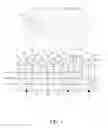
FIG. 2 is an illustrative first timing diagram of a liquid crystal panel driving circuit according to one embodiment of the present disclosure;
FIG. 3 is an illustrative second timing diagram of a liquid crystal panel driving circuit according to one embodiment of the present disclosure; and
FIG. 4 is an illustrative third timing diagram of a liquid crystal panel driving circuit according to one embodiment of the present disclosure.
DETAILED DESCRIPTION OF THE PREFERRED EMBODIMENTS
The following embodiments refer to the accompanying drawings for exemplifying specific implementable embodiments of the present disclosure. The foregoing preferred embodiments of the present disclosure are illustrative rather than limiting of the present disclosure. It is intended that they cover various modifications and similar arrangements be included within the spirit and scope of the present disclosure.
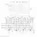
FIG. 1 is an illustrative structure diagram of a liquid crystal panel driving circuit according to one embodiment of the present disclosure. In FIG. 1, the liquid crystal panel driving circuit includes an array substrate 101 arranged by a plurality of sub-pixel units 1011, a data driver 102, a switch unit 103, and a plurality of data lines D1-D12 (e.g., twelve data lines) and scan lines G1-G4 (e.g., four scan lines) formed between a plurality of columns and rows of the sub-pixel units 1011.
Each of the sub-pixel unit columns is coupled to one scan line, and each of the sub-pixel unit rows is coupled to one data line. Every three sub-pixel unit columns are defined as a row cycle that includes a first data line M1, a second data line M2, and a third data line M3 coupled to a same data driving signal output line of the data driver 102 via the switch unit 103.
The switch unit 103 includes a first control switch T1, a second control switch T2 and a third control switch T3. The first terminals of the first control switch T1, the second control switch T2 and the third control switch T3 are coupled to the same data driving signal output line of the data driver 102. A second terminal of the first control switch T1 is coupled to the first data line M1, a second terminal of the second control switch T2 is coupled to the second data line M2, and a second terminal of the third control switch T3 is coupled to the third data line M3. A control terminal of the first control switch T1 is configured to receive a first control signal MUX1, a control terminal of the second control switch T2 is configured to receive a second control signal MUX2, and a control terminal of the third control switch T3 is configured to receive a third control signal MUX3.
In one embodiment, the first control switch T1, the second control switch T2 and the third control switch T3 are a thin film transistor. The first terminal, the second terminal and the control terminal of the first control switch T1, the second control switch T2 and the third control switch T3 are a source electrode, a drain electrode and a gate electrode.
In detail, in a first row cycle 104, the first data line M1 is a first data wire D1 on the array substrate 101, the second data line M2 is a sixth data wire D6 on the array substrate 101, and the third data line M3 is a third data wire D3 on the array substrate 101. In a second row cycle 105, the first data line M1 is a fourth data wire D4 on the array substrate 101, the second data line M2 is a fifth data wire D5 on the array substrate 101, and the third data line M3 is a second data wire D2 on the array substrate 101. In a third row cycle 106, the first data line M1 is a eleventh data wire D11 on the array substrate 101, the second data line M2 is a eighth data wire D8 on the array substrate 101, and the third data line M3 is a ninth data wire D9 on the array substrate 101. In a fourth row cycle 107, the first data line M1 is a tenth data wire D10 on the array substrate 101, the second data line M2 is a seventh data wire D7 on the array substrate 101, and the third data line M3 is a twelfth data wire D12 on the array substrate 101. Persons skilled in the art can obtain a connection relationship of a whole liquid crystal panel according to the above connection relation.
For example, in the first row cycle 104, the first data line M1, the second data line M2 and the third data line M3 of the liquid crystal panel driving circuit in the present disclosure are connected to the same data driving signal output line of the data driver 102 via the first control switch T1, the second control switch T2 and the third control switch T3.
Since a data line of a earlier data signal output may be affected by a data line of a later data signal output, the switch unit 103 in the present disclosure is configured to control the first data line M1, the second data line M2, and the third data line M3 to output data signals in different output orders, such that a plurality of different data lines includes the same output order to improve the vertical lines on the liquid crystal display device and upgrade the display quality of the liquid crystal display device.
In one embodiment, the output orders of the data signals output by the first data line M1, the second data line M2, and the third data line M3 includes that the data signals are sequentially output by a first output order of the first data line, the second data line and the third data line, the data signals are sequentially output by a second output order of the third data line, the first data line and the second data line, and the data signals are sequentially output by a third output order of the second data line, the third data line and the first data line.
In one embodiment, the output orders of the data signals output by the first data line, the second data line and the third data line are switched once at a time period (i.e., a preset time period). The data signals are output according to the first output order during a (3n+1)th time period, the data signals are output according to the second output order during a (3n+2)th time period, and the data signals are output according to the third output order during a (3n+3)th time period, where n is an integer greater than zero.
FIG. 2 is an illustrative first timing diagram of a liquid crystal panel driving circuit according to one embodiment of the present disclosure. As shown in FIG. 2, the time period is defined as one frame of display time. The scan lines are driven from the first line to the last line by controlling the first control signal MUX1, the second control signal MUX2 and the third control signal MUX3. In a first frame, a fourth frame, a seventh frame, . . . , and a (3n+1)th frame, the data signals are sequentially output by a first output order of the first data line, the second data line and the third data line. In a second frame, a fifth frame, a eighth frame, . . . , and a (3n+2)th frame, the data signals are sequentially output by a second output order of the third data line, the first data line and the second data line. In a third frame, a sixth frame, a ninth frame, . . . , and a (3n+3)th frame, the data signals are sequentially output by a third output order of the second data line, the third data line and the first data line.
FIG. 3 is an illustrative second timing diagram of a liquid crystal panel driving circuit according to one embodiment of the present disclosure. As shown in FIG. 3, the time period is defined as two frames of display time. The scan lines are driven from the first line to the last line by controlling the first control signal MUX1, the second control signal MUX2 and the third control signal MUX3. In a first frame, a second frame, a seventh frame, a eighth frame, . . . , a (3n+1)th frame and a (3n+2)th frame, the data signals are sequentially output by a first output order of the first data line, the second data line and the third data line. In a third frame, a fourth frame, a ninth frame, a tenth frame, . . . , a (3n+3)th frame and a (3n+4)th frame, the data signals are sequentially output by a second output order of the third data line, the first data line and the second data line. In a fifth frame, a sixth frame, a eleventh frame, a twelfth frame, . . . , a (3n+5)th frame and a (3n+6)th frame, the data signals are sequentially output by a third output order of the second data line, the third data line and the first data line.
In one embodiment, the polarities of sub-units 1011 in a first frame, a third frame, . . . , and a (2n+1)th frame display time are inverse to the polarities of sub-units 1011 in a second frame, a fourth frame, . . . , and a (2n+2)th frame display time so that display driving operations are more balanced to improve a display quality.
FIG. 4 is an illustrative third timing diagram of a liquid crystal panel driving circuit according to one embodiment of the present disclosure. As shown in FIG. 4, the time period is defined as one-tenth frame of display time. The scan lines are driven from the first line to the last line by controlling the first control signal MUX1, the second control signal MUX2 and the third control signal MUX3. In a first frame, a fourth frame, a seventh frame, . . . , and a (3n+1)th frame, the data signals are sequentially output by a first output order of the first data line, the second data line and the third data line. In a second frame, a fifth frame, a eighth frame, . . . , and a (3n+2)th frame, the data signals are sequentially output by a second output order of the third data line, the first data line and the second data line. In a third frame, a sixth frame, a ninth frame, . . . , and a (3n+3)th frame, the data signals are sequentially output by a third output order of the second data line, the third data line and the first data line.
In at least one embodiment, the present disclosure provides a liquid crystal panel driving circuit and a liquid crystal display device by changing the output orders of the data signals of the first data line, the second data line, and the third data line, such that the superposition of the data signals of the first data line, the second data line, and the third data line using a plurality of time periods to improve the vertical lines on the liquid crystal display device and upgrade the display quality of the liquid crystal display device.
The present disclosure further provides a liquid crystal display device including the above liquid crystal panel driving circuit, which will not be repeated here.
The present disclosure provides a liquid crystal panel driving circuit and a liquid crystal display device by changing the output orders of the data signals of the first data line, the second data line, and the third data line, such that the superposition of the data signals of the first data line, the second data line, and the third data line using a plurality of time periods to improve the vertical lines on the liquid crystal display device and upgrade the display quality of the liquid crystal display device.
As is understood by a person skilled in the art, the foregoing preferred embodiments of the present disclosure are illustrative rather than limiting of the present disclosure. It is intended that they cover various modifications and similar arrangements be included within the spirit and scope of the present disclosure, the scope of which should be accorded the broadest interpretation so as to encompass all such modifications and similar structures.
Claims
What is claimed is:1. A liquid crystal panel driving circuit, comprising an array substrate arranged by a plurality of sub-pixel units, a data driver, a switch unit, and a plurality of data lines and scan lines formed between a plurality of sub-pixel unit columns and sub-pixel unit rows;
wherein each of the sub-pixel unit columns is coupled to one scan line, each of the sub-pixel unit rows is coupled to one data line, every three sub-pixel unit columns are defined as a row cycle that comprises a first data line, a second data line, and a third data line coupled to a same data driving signal output line of the data driver via the switch unit;
wherein the switch unit is configured to control the first data line, the second data line, and the third data line to output data signals in different output orders;
wherein the switch unit comprises a first control switch, a second control switch and a third control switch;
wherein first terminals of the first control switch, the second control switch and the third control switch are coupled to the same data driving signal output line of the data driver;
wherein a second terminal of the first control switch is coupled to the first data line, a second terminal of the second control switch is coupled to the second data line, and a second terminal of the third control switch is coupled to the third data line;
wherein a control terminal of the first control switch is configured to receive a first control signal, a control terminal of the second control switch is configured to receive a second control signal, and a control terminal of the third control switch is configured to receive a third control signal;
wherein the output orders of the data signals which are output by the first data line, the second data line, and the third data line comprises:
the data signals are sequentially output by a first output order of the first data line, the second data line and the third data line;
the data signals are sequentially output by a second output order of the third data line, the first data line and the second data line; and
the data signals are sequentially output by a third output order of the second data line, the third data line and the first data line.
2. The liquid crystal panel driving circuit of claim 1, wherein the first control switch, the second control switch and the third control switch are a thin film transistor, and the first terminal, the second terminal and the control terminal of the first control switch, the second control switch and the third control switch are a source electrode, a drain electrode and a gate electrode.
3. The liquid crystal panel driving circuit of claim 1, wherein the output orders of the data signals output by the first data line, the second data line and the third data line are switched once at a time period, wherein the data signals are output according to the first output order during a (3n+1)th time period, the data signals are output according to the second output order during a (3n+2)th time period, the data signals are output according to the third output order during a (3n+3)th time period, and wherein n is an integer greater than zero.
4. A liquid crystal panel driving circuit, comprising an array substrate arranged by a plurality of sub-pixel units, a data driver, a switch unit, and a plurality of data lines and scan lines formed between a plurality of sub-pixel unit columns and sub-pixel unit rows;
wherein each of the sub-pixel unit columns is coupled to one scan line, each of the sub-pixel unit rows is coupled to one data line, every three sub-pixel unit columns are defined as a row cycle that comprises a first data line, a second data line, and a third data line coupled to a same data driving signal output line of the data driver via the switch unit;
wherein the switch unit is configured to control the first data line, the second data line, and the third data line to output data signals in different output orders.
5. The liquid crystal panel driving circuit of claim 4, wherein the switch unit comprises a first control switch, a second control switch and a third control switch;
wherein first terminals of the first control switch, the second control switch and the third control switch are coupled to the same data driving signal output line of the data driver;
wherein a second terminal of the first control switch is coupled to the first data line, a second terminal of the second control switch is coupled to the second data line, and a second terminal of the third control switch is coupled to the third data line; and
wherein a control terminal of the first control switch is configured to receive a first control signal, a control terminal of the second control switch is configured to receive a second control signal, and a control terminal of the third control switch is configured to receive a third control signal.
6. The liquid crystal panel driving circuit of claim 5, wherein the first control switch, the second control switch and the third control switch are a thin film transistor, and the first terminal, the second terminal and the control terminal of the first control switch, the second control switch and the third control switch are a source electrode, a drain electrode and a gate electrode.
7. The liquid crystal panel driving circuit of claim 4, wherein the output orders of the data signals which are output by the first data line, the second data line, and the third data line comprises:
the data signals are sequentially output by a first output order of the first data line, the second data line and the third data line;
the data signals are sequentially output by a second output order of the third data line, the first data line and the second data line; and
the data signals are sequentially output by a third output order of the second data line, the third data line and the first data line.
8. The liquid crystal panel driving circuit of claim 7, wherein the output orders of the data signals output by the first data line, the second data line and the third data line are switched once at a preset time period, wherein the data signals are output according to the first output order during a (3n+1)th time period, the data signals are output according to the second output order during a (3n+2)th time period, the data signals are output according to the third output order during a (3n+3)th time period, and wherein n is an integer greater than zero.
9. A liquid crystal display device comprising a liquid crystal panel driving circuit, wherein the liquid crystal panel driving circuit comprises an array substrate arranged by a plurality of sub-pixel units, a data driver, a switch unit, and a plurality of data lines and scan lines formed between a plurality of sub-pixel unit columns and sub-pixel unit rows;
wherein each of the sub-pixel unit columns is coupled to one scan line, each of the sub-pixel unit rows is coupled to one data line, every three sub-pixel unit columns are defined as a row cycle that comprises a first data line, a second data line, and a third data line coupled to a same data driving signal output line of the data driver via the switch unit;
wherein the switch unit is configured to control the first data line, the second data line, and the third data line to output data signals in different output orders.
10. The liquid crystal display device of claim 9, wherein the switch unit comprises a first control switch, a second control switch and a third control switch;
wherein first terminals of the first control switch, the second control switch and the third control switch are coupled to the same data driving signal output line of the data driver;
wherein a second terminal of the first control switch is coupled to the first data line, a second terminal of the second control switch is coupled to the second data line, and a second terminal of the third control switch is coupled to the third data line; and
wherein a control terminal of the first control switch is configured to receive a first control signal, a control terminal of the second control switch is configured to receive a second control signal, and a control terminal of the third control switch is configured to receive a third control signal.
11. The liquid crystal display device of claim 10, wherein the first control switch, the second control switch and the third control switch are a thin film transistor, and the first terminal, the second terminal and the control terminal of the first control switch, the second control switch and the third control switch are a source electrode, a drain electrode and a gate electrode.
12. The liquid crystal display device of claim 9, wherein the output orders of the data signals which are output by the first data line, the second data line, and the third data line comprises:
the data signals are sequentially output by a first output order of the first data line, the second data line and the third data line;
the data signals are sequentially output by a second output order of the third data line, the first data line and the second data line; and
the data signals are sequentially output by a third output order of the second data line, the third data line and the first data line.
13. The liquid crystal display device of claim 12, wherein the output orders of the data signals output by the first data line, the second data line and the third data line are switched once at a preset time period, wherein the data signals are output according to the first output order during a (3n+1)th time period, the data signals are output according to the second output order during a (3n+2)th time period, the data signals are output according to the third output order during a (3n+3)th time period, and wherein n is an integer greater than zero.
Images & Drawings included:
Sources:
- United States Patent and Trademark Office - verify current appl. status at the USPTO↗
Similar patent applications:
- » 20100325466
DISPLAY PANEL DRIVE CIRCUIT, LIQUID CRYSTAL DISPLAY DEVICE, AND METHOD FOR DRIVING DISPLAY PANEL - » 20110001752
DISPLAY PANEL DRIVE CIRCUIT, LIQUID CRYSTAL DISPLAY DEVICE, AND METHOD FOR DRIVING DISPLAY PANEL - » 20190096351
Array substrate comprising switch connected between two adjacent scan lines and switch drive circuit, liquid crystal display device, display panel and method for driving display panel - » 20190272795
Liquid crystal panel driving circuit and liquid crystal display device - » 20130044085
Liquid crystal panel driving circuit and liquid crystal display Device Using the Same - » 20180210261
LIQUID CRYSTAL PANEL DRIVE CIRCUIT AND LIQUID CRYSTAL DISPLAY DEVICE - » 20100321623
Display panel, liquid crystal display device and drive-circuit-mounted board - » 20060012591
Liquid crystal display device and driving circuit for liquid crystal panel with a memory effect - » 20180218707
Gate voltage driving device, method, driving circuit, and liquid crystal display panel - » 10669863
Display panel driving method, display panel driver circuit, and liquid crystal display device
Recent applications in this class:
- » 20250266012 2025-08-21
DRIVER CIRCUIT AND IMAGE DISPLAY SYSTEM - » 20250210006 2025-06-26
ELECTRO-OPTICAL DEVICE AND ELECTRONIC EQUIPMENT - » 20250174209 2025-05-29
DATA INTEGRATED CIRCUIT AND DISPLAY DEVICE INCLUDING THE SAME - » 20250111834 2025-04-03
LIQUID CRYSTAL DISPLAY DEVICE AND METHOD OF DRIVING THE SAME - » 20250095602 2025-03-20
DISPLAY DEVICE AND ELECTRONIC DEVICE - » 20250095601 2025-03-20
SOURCE DRIVER AND DISPLAY DEVICE - » 20250078774 2025-03-06
DISPLAY DEVICE - » 20250054458 2025-02-13
BUFFER AND A DATA DRIVING DEVICE - » 20250046268 2025-02-06
LIQUID CRYSTAL DISPLAY APPARATUS AND METHOD FOR CONTROLLING THE SAME - » 20240420660 2024-12-19
STRUCTURE OF STABLE CRYSTAL LIQUID DISPLAY MODULE CAPABLE OF REDUCING CROSSTALK INTERFERENCE
Recent applications for this Assignee:
- » 20250252896 2025-08-07
PIXEL DRIVING CIRCUIT AND DISPLAY PANEL - » 20250248193 2025-07-31
DISPALY PANEL AND DISPLAY MODULE - » 20250244850 2025-07-31
TOUCH DISPLAY DEVICES AND TOUCH METHODS THEREOF - » 20250244577 2025-07-31
DISPLAY MODULE AND FIELD-OF-VIEW DISPLAY DEVICE FOR VEHICLE - » 20250225913 2025-07-10
LIGHT BOARDS AND DISPLAY PANELS - » 20250221126 2025-07-03
DISPLAY BACKPLANE AND DISPLAY DEVICE - » 20250212512 2025-06-26
DISPLAY PANEL - » 20250210003 2025-06-26
DISPLAY DEVICE AND ELECTRONIC DEVICE - » 20250182713 2025-06-05
GOA CIRCUIT AND DISPLAY PANEL - » 20250159934 2025-05-15
TRANSISTOR STRUCTURES, DRIVING SUBSTRATES AND DISPLAY PANELS