Light emitting diode display and manufacture method thereof
US20180301442A1
2018-10-18
15/519,839
2017-03-16
✅ Patent granted
US 10,276,550 B2
2019-04-30
WO; PCT/CN2017/076861; 20170316
WO; WO2018/152895; 20180830
Phuc Dang
Leong C. Lei
2037-05-30
Abstract:
The present invention provides a light emitting diode display and a manufacture method thereof. The manufacture method of the light emitting diode forms the first anode covering the first through hole and possessing the reflection property on the planarization layer, and can use the reflection property of the first anode to gather and reflect the divergent light emitted by the light emitting diode located inside the first through hole to raise the light utilization and to promote the display quality. The light emitting diode of the present invention locates the first anode covering the first through hole and possessing the reflection property on the planarization layer, and can use the reflection property of the first anode to gather and reflect the divergent light emitted by the light emitting diode located inside the first through hole to raise the light utilization and to promote the display quality.
Inventors:
- Baixiang Han 61 🇨🇳 Shenzhen, China
- Baixiang Han 25 🇨🇳 Shenzhen City, China
- Poyen Lu 3 🇨🇳 Shenzhen City, China
- Poyen Lu 14 🇨🇳 Shenzhen, China
Assignee:
- Shenzhen China Star Optoelectronics Technology Co Ltd. 3,202 🇨🇳 Shenzhen, Guangdong, China
- SHENZHEN CHINA STAR OPTOELECTRONICS TECHNOLOGY CO., LTD. 78 🇨🇳 Shenzhen City, China
Applicant:
Interested in similar patents?
Get notified when new applications in this technology area are published.
Classification:
H01L25/167 » CPC main
Assemblies consisting of a plurality of individual semiconductor or other solid state devices ; Multistep manufacturing processes thereof the devices being of types provided for in two or more different main groups of - , e.g. forming hybrid circuits comprising optoelectronic devices, e.g. LED, photodiodes
H01L27/124 » CPC further
Devices consisting of a plurality of semiconductor or other solid-state components formed in or on a common substrate including semiconductor components specially adapted for rectifying, oscillating, amplifying or switching and having at least one potential-jump barrier or surface barrier; including integrated passive circuit elements with at least one potential-jump barrier or surface barrier the substrate being other than a semiconductor body, e.g. an insulating body comprising a plurality of TFTs formed on a non-semiconducting substrate, e.g. driving circuits for AMLCDs with a particular composition, shape or layout of the wiring layers specially adapted to the circuit arrangement, e.g. scanning lines in LCD pixel circuits
H01L27/1248 » CPC further
Devices consisting of a plurality of semiconductor or other solid-state components formed in or on a common substrate including semiconductor components specially adapted for rectifying, oscillating, amplifying or switching and having at least one potential-jump barrier or surface barrier; including integrated passive circuit elements with at least one potential-jump barrier or surface barrier the substrate being other than a semiconductor body, e.g. an insulating body comprising a plurality of TFTs formed on a non-semiconducting substrate, e.g. driving circuits for AMLCDs with a particular composition or shape of the interlayer dielectric specially adapted to the circuit arrangement
H01L27/1262 » CPC further
Devices consisting of a plurality of semiconductor or other solid-state components formed in or on a common substrate including semiconductor components specially adapted for rectifying, oscillating, amplifying or switching and having at least one potential-jump barrier or surface barrier; including integrated passive circuit elements with at least one potential-jump barrier or surface barrier the substrate being other than a semiconductor body, e.g. an insulating body comprising a plurality of TFTs formed on a non-semiconducting substrate, e.g. driving circuits for AMLCDs; Multistep manufacturing methods with a particular formation, treatment or coating of the substrate
H01L33/405 » CPC further
Semiconductor devices with at least one potential-jump barrier or surface barrier specially adapted for light emission; Processes or apparatus specially adapted for the manufacture or treatment thereof or of parts thereof; Details thereof characterised by the electrodes; Materials therefor Reflective materials
H01L51/5209 » CPC further
Solid state devices using organic materials as the active part, or using a combination of organic materials with other materials as the active part; Processes or apparatus specially adapted for the manufacture or treatment of such devices, or of parts thereof specially adapted for light emission, e.g. organic light emitting diodes [OLED] or polymer light emitting devices [PLED]; Details of devices; Electrodes; Anodes, i.e. with high work-function material characterised by the shape
H01L2933/0016 » CPC further
Details relating to devices covered by the group but not provided for in its subgroups; Processes relating to electrodes
H01L2933/0025 » CPC further
Details relating to devices covered by the group but not provided for in its subgroups; Processes relating to coatings
H01L2933/0066 » CPC further
Details relating to devices covered by the group but not provided for in its subgroups; Processes relating to semiconductor body packages relating to arrangements for conducting electric current to or from the semiconductor body
H01L25/16 IPC
Assemblies consisting of a plurality of individual semiconductor or other solid state devices ; Multistep manufacturing processes thereof the devices being of types provided for in two or more different main groups of - , e.g. forming hybrid circuits
H01L27/12 IPC
Devices consisting of a plurality of semiconductor or other solid-state components formed in or on a common substrate including semiconductor components specially adapted for rectifying, oscillating, amplifying or switching and having at least one potential-jump barrier or surface barrier; including integrated passive circuit elements with at least one potential-jump barrier or surface barrier the substrate being other than a semiconductor body, e.g. an insulating body
H01L33/40 IPC
Semiconductor devices with at least one potential-jump barrier or surface barrier specially adapted for light emission; Processes or apparatus specially adapted for the manufacture or treatment thereof or of parts thereof; Details thereof characterised by the electrodes Materials therefor
H01L33/44 » CPC further
Semiconductor devices with at least one potential-jump barrier or surface barrier specially adapted for light emission; Processes or apparatus specially adapted for the manufacture or treatment thereof or of parts thereof; Details thereof characterised by the coatings, e.g. passivation layer or anti-reflective coating
H01L33/62 » CPC further
Semiconductor devices with at least one potential-jump barrier or surface barrier specially adapted for light emission; Processes or apparatus specially adapted for the manufacture or treatment thereof or of parts thereof; Details thereof characterised by the semiconductor body packages Arrangements for conducting electric current to or from the semiconductor body, e.g. lead-frames, wire-bonds or solder balls
H01L33/42 » CPC further
Semiconductor devices with at least one potential-jump barrier or surface barrier specially adapted for light emission; Processes or apparatus specially adapted for the manufacture or treatment thereof or of parts thereof; Details thereof characterised by the electrodes; Materials therefor Transparent materials
H01L51/52 IPC
Solid state devices using organic materials as the active part, or using a combination of organic materials with other materials as the active part; Processes or apparatus specially adapted for the manufacture or treatment of such devices, or of parts thereof specially adapted for light emission, e.g. organic light emitting diodes [OLED] or polymer light emitting devices [PLED] Details of devices
H01L51/56 » CPC further
Solid state devices using organic materials as the active part, or using a combination of organic materials with other materials as the active part; Processes or apparatus specially adapted for the manufacture or treatment of such devices, or of parts thereof specially adapted for light emission, e.g. organic light emitting diodes [OLED] or polymer light emitting devices [PLED] Processes or apparatus specially adapted for the manufacture or treatment of such devices or of parts thereof
H01L51/5271 » CPC further
Solid state devices using organic materials as the active part, or using a combination of organic materials with other materials as the active part; Processes or apparatus specially adapted for the manufacture or treatment of such devices, or of parts thereof specially adapted for light emission, e.g. organic light emitting diodes [OLED] or polymer light emitting devices [PLED]; Details of devices; Arrangements for extracting light from the device Reflective means
Description
FIELD OF THE INVENTION
The present invention relates to a display technology field, and more particularly to a light emitting diode display and a manufacture method thereof.
BACKGROUND OF THE INVENTION
With the progress of the technology, various display products have already been developed in the market, such as the Liquid Crystal Display (LCD), the Plasma Display Panel (PDP) and the Light Emitting Diode display (LED display). The LED display possesses the advantages of high luminous efficiency, long life and low energy consumption, and has been widely applied for the outdoor displays and the large outdoor billboards, and also exists in the displays of the home television and the computer.
The light emitting diode display is a display screen with a way of controlling the display of the semiconductor light emitting diode for showing kinds of information, such as words, graphics, images, animation, quotes, video and recording tape signals.
The technological progress of light emitting diodes is the biggest driving force to expand the market demand and application. At first, the light emitting diode is only used for micro indicator to be applied in the high-end equipments of the computer, audio and video recorders. With the development of large scale integrated circuits and computer technology, the light emitting diode displays are rapidly rising and gradually expanded in the fields of stock quotes, digital cameras, personal digital assistant (PDA), and mobile phones.
The LED display integrates the microelectronics technology, the computer technology, the information process in one, and possesses advantages of colorfulness, wide dynamic range, high brightness, high resolution, low operating voltage, low power consumption, long life, impact resistance, and stable and reliable work to become the new generation display media with the most advantage. The light emitting diode display has been widely applied in the large square, commercial advertisement, sports venues, information dissemination, press release and securities trade for satisfying requirements of various environments.
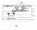
FIG. 1 is a structure diagram of a light emitting diode display according to prior art. As shown in FIG. 1, the light emitting diode display comprises a substrate 100, a thin film transistor (TFT) layer 200 located on the substrate 100, a first planarization layer 300 located on the TFT layer 200, a first anode 400 located on the first planarization layer 300, a second planarization layer 500 located on the first anode 400 and the first planarization layer 300, a first through hole 510 being located in the second planarization layer 500 and exposing the first anode 400, a light emitting diode 600 located inside the first through hole 51, a cathode insulation layer 720, which is around the light emitting diode 600 and on the first anode 400, located inside the first through hole 510, and a first cathode 730 located on the cathode insulation layer 720, the light emitting diode 600 and the second planarization layer 500;
the light emitting diode 600 comprises a luminous lamp 610 and a second anode 620 and a second cathode 630 respectively connected to two ends of the luminous lamp 610, and the second anode 620 connects with the first anode 400, and the second cathode 630 contacts with the first cathode 730, and the first anode 400 and the first cathode 730 are insulated by the cathode insulation layer 720.
In the aforesaid light emitting diode, the light emitted by the light emitting diode 600 possesses the divergent property, and the second planarization layer 500, where the light emitting diode 600 is located, is generally manufactured with the transparent organic photoresist material, thus the second planarization layer 500 cannot gather and reflect the divergent light emitted by the light emitting diode 600 to lead to the light leakage, to reduce the light utilization and to raise the display energy consumption.
SUMMARY OF THE INVENTION
An objective of the present invention is to provide a manufacture method of a light emitting diode display, which can raise the light utilization of the light emitting diode to promote the display quality.
Another objective of the present invention is to provide a light emitting diode display, of which the light utilization is better to possess the better display quality.
For realizing the aforesaid objectives, the present invention first provides a manufacture method of a light emitting diode display, comprising steps of:
step 1, providing a TFT backplate, and the TFT backplate comprising a substrate, a TFT layer located on the substrate, a planarization layer located on the TFT layer and a first through hole located in the planarization layer; the TFT layer comprising a drain correspondingly located under the first through hole;
step 2, forming a first anode on the planarization layer, and the first anode covering the first through hole and contacting with the drain via the first through hole, and the first anode being a reflective electrode;
step 3, providing a light emitting diode, and the light emitting diode comprising a luminous lamp and a second anode and a second cathode respectively connected to two ends of the luminous lamp;
transferring the light emitting diode into the first through hole of the TFT backplate, and connecting the second anode of the light emitting diode with the first anode of the TFT backplate;
step 4, forming a cathode insulation layer, which is around the light emitting diode, on the first anode and the planarization layer, and a portion of the cathode insulation layer, which is located inside the first through hole, completely covering the second anode and at least exposing a top end of the second cathode;
step 5, forming a first cathode on the cathode insulation layer and the light emitting diode, and the first cathode contacting with the second cathode, and the first cathode and the first anode being insulated by the cathode insulation layer.
The TFT layer comprises a gate located on the substrate, a gate protection layer on the gate and the substrate, an active layer located on the gate protection layer, an etching stopper layer located on the active layer and the gate protection layer, and a source and a drain located on the etching stopper layer, and second through holes respectively corresponding to two ends of the active layer are configured in the etching stopper layer, and the source and the drain contact with the two ends of the active layer respectively via the second through holes.
A material of the first anode is metal.
A material of the first anode comprises one or more of molybdenum, aluminum, copper, titanium and chromium.
A material of the cathode insulation layer is organic insulation material; the first cathode is a transparent electrode.
The present invention further provides a light emitting diode display, comprising a substrate, a TFT layer located on the substrate, a planarization layer located on the TFT layer, a first through hole located in the planarization layer, a first anode being located on the planarization layer and covering the first through hole, a light emitting diode located inside the first through hole and on the first anode, a cathode insulation layer located on the first anode and the planarization layer and around the light emitting diode, and a first cathode located on the cathode insulation layer and the light emitting diode;
the TFT layer comprising a drain correspondingly located under the first through hole, and the first anode contacting with the drain via the first through hole;
the light emitting diode comprising a luminous lamp and a second anode and a second cathode respectively connected to two ends of the luminous lamp, and the second anode connecting with the first anode, and the second cathode contacting with the first cathode;
a portion of the cathode insulation layer, which is located inside the first through hole, completely covering the second anode and at least exposing a top end of the second cathode, and the first anode and the first cathode being insulated by the cathode insulation layer;
the first anode is a reflective electrode.
The TFT layer comprises a gate located on the substrate, a gate protection layer on the gate and the substrate, an active layer located on the gate protection layer, an etching stopper layer located on the active layer and the gate protection layer, and a source and a drain located on the etching stopper layer, and second through holes respectively corresponding to two ends of the active layer are configured in the etching stopper layer, and the source and the drain contact with the two ends of the active layer respectively via the second through holes.
A material of the first anode is metal.
A material of the first anode comprises one or more of molybdenum, aluminum, copper, titanium and chromium.
A material of the cathode insulation layer is organic insulation material; the first cathode is a transparent electrode.
The present invention further provides a light emitting diode display, comprising a substrate, a TFT layer located on the substrate, a planarization layer located on the TFT layer, a first through hole located in the planarization layer, a first anode being located on the planarization layer and covering the first through hole, a light emitting diode located inside the first through hole and on the first anode, a cathode insulation layer located on the first anode and the planarization layer and around the light emitting diode, and a first cathode located on the cathode insulation layer and the light emitting diode;
the TFT layer comprising a drain correspondingly located under the first through hole, and the first anode contacting with the drain via the first through hole;
the light emitting diode comprising a luminous lamp and a second anode and a second cathode respectively connected to two ends of the luminous lamp, and the second anode connecting with the first anode, and the second cathode contacting with the first cathode;
a portion of the cathode insulation layer, which is located inside the first through hole, completely covering the second anode and at least exposing a top end of the second cathode, and the first anode and the first cathode being insulated by the cathode insulation layer;
the first anode is a reflective electrode;
wherein the TFT layer comprises a gate located on the substrate, a gate protection layer on the gate and the substrate, an active layer located on the gate protection layer, an etching stopper layer located on the active layer and the gate protection layer, and a source and a drain located on the etching stopper layer, and second through holes respectively corresponding to two ends of the active layer are configured in the etching stopper layer, and the source and the drain contact with the two ends of the active layer respectively via the second through holes;
wherein a material of the first anode is metal.
The benefits of the present invention are: the present invention provides a manufacture method of a light emitting diode, and the method forms the first anode covering the first through hole and possessing the reflection property on the planarization layer, and can use the reflection property of the first anode to gather and reflect the divergent light emitted by the light emitting diode located inside the first through hole to raise the light utilization and to promote the display quality. The light emitting diode provided by the present invention locates the first anode covering the first through hole and possessing the reflection property on the planarization layer, and can use the reflection property of the first anode to gather and reflect the divergent light emitted by the light emitting diode located inside the first through hole to raise the light utilization and to promote the display quality.
In order to better understand the characteristics and technical aspect of the invention, please refer to the following detailed description of the present invention is concerned with the diagrams, however, provide reference to the accompanying drawings and description only and is not intended to be limiting of the invention.
BRIEF DESCRIPTION OF THE DRAWINGS
The technical solution and the beneficial effects of the present invention are best understood from the following detailed description with reference to the accompanying figures and embodiments.
In drawings,
FIG. 1 is a structure diagram of a light emitting diode display according to prior art;
FIG. 2 is a flowchart of a manufacture method of a light emitting diode display according to the present invention;
FIG. 3 is a diagram of step 1 of a manufacture method of a light emitting diode display according to the present invention;
FIG. 4 is a diagram of step 2 of a manufacture method of a light emitting diode display according to the present invention;
FIG. 5 is a diagram of step 3 of a manufacture method of a light emitting diode display according to the present invention;
FIG. 6 is a diagram of step 4 of a manufacture method of a light emitting diode display according to the present invention;
FIG. 7 is a diagram of step 5 of a manufacture method of a light emitting diode display according to the present invention and also a structure diagram of a light emitting diode display according to the present invention.
DETAILED DESCRIPTION OF PREFERRED EMBODIMENTS
For better explaining the technical solution and the effect of the present invention, the present invention will be further described in detail with the accompanying drawings and the specific embodiments.
Please refer to FIG. 2, the present invention first provides a manufacture method of a light emitting diode display, comprising steps of:
step 1, as shown in FIG. 3, providing a TFT backplate 80, and the TFT backplate 80 comprising a substrate 10, a TFT layer 20 located on the substrate 10, a planarization layer 30 located on the TFT layer 20 and a first through hole 31 located in the planarization layer 30; the TFT layer 20 comprising a drain 26 correspondingly located under the first through hole 31.
Specifically, the TFT layer 20 comprises a gate 21 located on the substrate 10, a gate protection layer 22 on the gate 21 and the substrate 10, an active layer 23 located on the gate protection layer 22, an etching stopper layer 24 located on the active layer 23 and the gate protection layer 22, and a source 25 and a drain 26 located on the etching stopper layer 24, and second through holes 242 respectively corresponding to two ends of the active layer 23 are configured in the etching stopper layer 24, and the source 25 and the drain 26 contact with the two ends of the active layer 23 respectively via the second through holes 242.
step 2, as shown in FIG. 4, forming a first anode 40 on the planarization layer 30, and the first anode 40 covering the first through hole 31 and contacting with the drain 26 via the first through hole 31, and the first anode 40 being a reflective electrode.
Specifically, a material of the first anode 40 is metal.
Preferably, the material of the first anode 40 comprises one or more of molybdenum (Mo), aluminum (Al), copper (Cu), titanium (Ti) and chromium (Cr).
step 3, as shown in FIG. 5, providing a light emitting diode 60, and the light emitting diode 60 comprising a luminous lamp 61 and a second anode 62 and a second cathode 63 respectively connected to two ends of the luminous lamp 61;
transferring the light emitting diode 60 into the first through hole 31 of the TFT backplate 80, and connecting the second anode 62 of the light emitting diode 60 with the first anode 40 of the TFT backplate 80.
Specifically, in step 3, welding is used to connect the second anode 62 of the light emitting diode 60 with the first anode 40 of the TFT backplate 80.
Because the first anode 40 is a reflective electrode, it can gather and reflect the divergent light emitted by the light emitting diode 60 to raise the light utilization.
step 4, as shown in FIG. 6, forming a cathode insulation layer 72, which is around the light emitting diode 60, on the first anode 40 and the planarization layer 30, and a portion of the cathode insulation layer 72, which is located inside the first through hole 31, completely covering the second anode 62 and at least exposing a top end of the second cathode 63.
The cathode insulation layer 72 is insulation material. Thus, the first anode 40 can be insulated from the first cathode 73 manufactured thereafter to prevent the short circuit.
Specifically, in step 4, ink jet printing can be used to form the cathode insulation layer 72, or a combination of the organic material coating process and the photolithography process can be used to form the cathode insulation layer 72.
Preferably, a material of the cathode insulation layer 72 is organic insulation material.
step 5, as shown in FIG. 7, forming a first cathode 73 on the cathode insulation layer 72 and the light emitting diode 60, and the first cathode 73 contacting with the second cathode 63, and the first cathode 73 and the first anode 40 being insulated by the cathode insulation layer 72.
Specifically, in step 5, evaporation is used to form the first cathode 73.
Specifically, the first anode 73 is a transparent electrode.
Preferably, a material of the first cathode 73 is transparent conductive metal oxide, such as indium tin oxide (ITO).
Under the circumstance that the first anode 40 is a reflective electrode and the first anode 73 is a transparent electrode, the light emitting diode of the present invention constructs the top emitting light emitting diode display, and one side of the first anode 73 is the illuminating surface.
The aforesaid manufacture method of the light emitting diode forms the first anode 40 covering the first through hole 31 and possessing the reflection property on the planarization layer 30, and can use the reflection property of the first anode 40 to gather and reflect the divergent light emitted by the light emitting diode 60 located inside the first through hole 31 to raise the light utilization and to promote the display quality.
Please refer to FIG. 7. On the basis of the aforesaid manufacture method of the light emitting diode display, the present invention further provides a light emitting diode display, comprising a substrate 10, a TFT layer 20 located on the substrate 10, a planarization layer 30 located on the TFT layer 20, a first through hole 31 located in the planarization layer 30, a first anode 40 being located on the planarization layer 30 and covering the first through hole 31, a light emitting diode 60 located inside the first through hole 31 and on the first anode 40, a cathode insulation layer 72 located on the first anode 40 and the planarization layer 30 and around the light emitting diode 60, and a first cathode 73 located on the cathode insulation layer 72 and the light emitting diode 60;
the TFT layer 20 comprising a drain 26 correspondingly located under the first through hole 31, and the first anode 40 contacting with the drain 26 via the first through hole 31;
the light emitting diode 60 comprising a luminous lamp 61 and a second anode 62 and a second cathode 63 respectively connected to two ends of the luminous lamp 61, and the second anode 62 connecting with the first anode 40, and the second cathode 63 contacting with the first cathode 73;
a portion of the cathode insulation layer 72, which is located inside the first through hole 31, completely covering the second anode 62 and at least exposing a top end of the second cathode 63, and the first anode 40 and the first cathode 73 being insulated by the cathode insulation layer 72;
The first anode 40 is a reflective electrode and can gather and reflect the divergent light emitted by the light emitting diode 60 to raise the light utilization.
Specifically, the TFT layer 20 comprises a gate 21 located on the substrate 10, a gate protection layer 22 on the gate 21 and the substrate 10, an active layer 23 located on the gate protection layer 22, an etching stopper layer 24 located on the active layer 23 and the gate protection layer 22, and a source 25 and a drain 26 located on the etching stopper layer 24, and second through holes 242 respectively corresponding to two ends of the active layer 23 are configured in the etching stopper layer 24, and the source 25 and the drain 26 contact with the two ends of the active layer 23 respectively via the second through holes 242.
Specifically, a material of the first anode 40 is metal.
Preferably, the material of the first anode 40 comprises one or more of molybdenum (Mo), aluminum (Al), copper (Cu), titanium (Ti) and chromium (Cr).
Preferably, a material of the cathode insulation layer 72 is organic insulation material.
Specifically, the first anode 73 is a transparent electrode.
Preferably, a material of the first cathode 73 is transparent conductive metal oxide, such as indium tin oxide (ITO).
The aforesaid light emitting diode locates the first anode 40 covering the first through hole 31 and possessing the reflection property on the planarization layer 30, and can use the reflection property of the first anode 40 to gather and reflect the divergent light emitted by the light emitting diode 60 located inside the first through hole 31 to raise the light utilization and to promote the display quality.
In conclusion, the present invention provides a light emitting diode display and a manufacture method thereof. The manufacture method of the light emitting diode according to the present invention forms the first anode covering the first through hole and possessing the reflection property on the planarization layer, and can use the reflection property of the first anode to gather and reflect the divergent light emitted by the light emitting diode located inside the first through hole to raise the light utilization and to promote the display quality. The light emitting diode of the present invention locates the first anode covering the first through hole and possessing the reflection property on the planarization layer, and can use the reflection property of the first anode to gather and reflect the divergent light emitted by the light emitting diode located inside the first through hole to raise the light utilization and to promote the display quality.
Above are only specific embodiments of the present invention, the scope of the present invention is not limited to this, and to any persons who are skilled in the art, change or replacement which is easily derived should be covered by the protected scope of the invention. Thus, the protected scope of the invention should go by the subject claims.
Claims
What is claimed is:1. A manufacture method of a light emitting diode display, comprising steps of:
step 1, providing a TFT backplate, and the TFT backplate comprising a substrate, a TFT layer located on the substrate, a planarization layer located on the TFT layer and a first through hole located in the planarization layer; the TFT layer comprising a drain correspondingly located under the first through hole;
step 2, forming a first anode on the planarization layer, and the first anode covering the first through hole and contacting with the drain via the first through hole, and the first anode being a reflective electrode;
step 3, providing a light emitting diode, and the light emitting diode comprising a luminous lamp and a second anode and a second cathode respectively connected to two ends of the luminous lamp;
transferring the light emitting diode into the first through hole of the TFT backplate, and connecting the second anode of the light emitting diode with the first anode of the TFT backplate;
step 4, forming a cathode insulation layer, which is around the light emitting diode, on the first anode and the planarization layer, and a portion of the cathode insulation layer, which is located inside the first through hole, completely covering the second anode and at least exposing a top end of the second cathode;
step 5, forming a first cathode on the cathode insulation layer and the light emitting diode, and the first cathode contacting with the second cathode, and the first cathode and the first anode being insulated by the cathode insulation layer.
2. The manufacture method of the light emitting diode display according to claim 1, wherein the TFT layer comprises a gate located on the substrate, a gate protection layer on the gate and the substrate, an active layer located on the gate protection layer, an etching stopper layer located on the active layer and the gate protection layer, and a source and a drain located on the etching stopper layer, and second through holes respectively corresponding to two ends of the active layer are configured in the etching stopper layer, and the source and the drain contact with the two ends of the active layer respectively via the second through holes.
3. The manufacture method of the light emitting diode display according to claim 1, wherein a material of the first anode is metal.
4. The manufacture method of the light emitting diode display according to claim 3, wherein a material of the first anode comprises one or more of molybdenum, aluminum, copper, titanium and chromium.
5. The manufacture method of the light emitting diode display according to claim 1, wherein a material of the cathode insulation layer is organic insulation material; the first cathode is a transparent electrode.
6. A light emitting diode display, comprising a substrate, a TFT layer located on the substrate, a planarization layer located on the TFT layer, a first through hole located in the planarization layer, a first anode being located on the planarization layer and covering the first through hole, a light emitting diode located inside the first through hole and on the first anode, a cathode insulation layer located on the first anode and the planarization layer and around the light emitting diode, and a first cathode located on the cathode insulation layer and the light emitting diode;
the TFT layer comprising a drain correspondingly located under the first through hole, and the first anode contacting with the drain via the first through hole;
the light emitting diode comprising a luminous lamp and a second anode and a second cathode respectively connected to two ends of the luminous lamp, and the second anode connecting with the first anode, and the second cathode contacting with the first cathode;
a portion of the cathode insulation layer, which is located inside the first through hole, completely covering the second anode and at least exposing a top end of the second cathode, and the first anode and the first cathode being insulated by the cathode insulation layer;
the first anode is a reflective electrode.
7. The light emitting diode display according to claim 6, wherein the TFT layer comprises a gate located on the substrate, a gate protection layer on the gate and the substrate, an active layer located on the gate protection layer, an etching stopper layer located on the active layer and the gate protection layer, and a source and a drain located on the etching stopper layer, and second through holes respectively corresponding to two ends of the active layer are configured in the etching stopper layer, and the source and the drain contact with the two ends of the active layer respectively via the second through holes.
8. The light emitting diode display according to claim 6, wherein a material of the first anode is metal.
9. The light emitting diode display according to claim 8, wherein a material of the first anode comprises one or more of molybdenum, aluminum, copper, titanium and chromium.
10. The light emitting diode display according to claim 6, wherein a material of the cathode insulation layer is organic insulation material; the first cathode is a transparent electrode.
11. A light emitting diode display, comprising a substrate, a TFT layer located on the substrate, a planarization layer located on the TFT layer, a first through hole located in the planarization layer, a first anode being located on the planarization layer and covering the first through hole, a light emitting diode located inside the first through hole and on the first anode, a cathode insulation layer located on the first anode and the planarization layer and around the light emitting diode, and a first cathode located on the cathode insulation layer and the light emitting diode;
the TFT layer comprising a drain correspondingly located under the first through hole, and the first anode contacting with the drain via the first through hole;
the light emitting diode comprising a luminous lamp and a second anode and a second cathode respectively connected to two ends of the luminous lamp, and the second anode connecting with the first anode, and the second cathode contacting with the first cathode;
a portion of the cathode insulation layer, which is located inside the first through hole, completely covering the second anode and at least exposing a top end of the second cathode, and the first anode and the first cathode being insulated by the cathode insulation layer;
the first anode is a reflective electrode;
wherein the TFT layer comprises a gate located on the substrate, a gate protection layer on the gate and the substrate, an active layer located on the gate protection layer, an etching stopper layer located on the active layer and the gate protection layer, and a source and a drain located on the etching stopper layer, and second through holes respectively corresponding to two ends of the active layer are configured in the etching stopper layer, and the source and the drain contact with the two ends of the active layer respectively via the second through holes;
wherein a material of the first anode is metal.
12. The light emitting diode display according to claim 11, wherein a material of the first anode comprises one or more of molybdenum, aluminum, copper, titanium and chromium.
13. The light emitting diode display according to claim 11, wherein a material of the cathode insulation layer is organic insulation material; the first cathode is a transparent electrode.
Images & Drawings included:


Sources:
- United States Patent and Trademark Office - verify current appl. status at the USPTO↗
Similar patent applications:
- » 20190355929
Organic light emitting diode display panel, manufacturing method thereof, and organic light emitting diode display apparatus - » 20070134830
Drive film, drive package for organic light emitting diode display, method of manufacturing thereof, and organic light emitting diode display including the same - » 20210408437
Organic light-emitting diode display panel, manufacturing method thereof, and organic light-emitting diode display device - » 20180301514
Organic light-emitting diode display device and manufacturing method thereof, and organic light-emitting diode display - » 20200227500
Organic light emitting diode display substrate, manufacturing method thereof, and display device comprising organic light emitting diode display substrate - » 20230354636
ORGANIC LIGHT EMITTING DIODE, MANUFACTURING METHOD THEREOF, DISPLAY SUBSTRATE AND DISPLAY APPARATUS - » 20160027861
Organic light emitting diode display, manufacturing method thereof, and rotating device for circuit film - » 20140103315
Organic light emitting diode display, manufacturing method thereof, and rotating device for circuit film - » 20220123248
Quantum dot light emitting diode, manufacturing method thereof and display panel with electron contribution layer for injecting free electrons to light emitting layer - » 20060033099
Organic light emitting diode display and manufacturing method thereof
Recent applications in this class:
- » 20250293223 2025-09-18
ELECTRONIC PACKAGE AND MANUFACTURING METHOD THEREOF - » 20250293222 2025-09-18
SEMICONDUCTOR DEVICES AND METHODS OF MANUFACTURE - » 20250286035 2025-09-11
ELECTRONIC DEVICE - » 20250286034 2025-09-11
DISPLAY PANEL - » 20250286033 2025-09-11
DISPLAY PANEL AND DISPLAY DEVICE - » 20250286032 2025-09-11
DISPLAY PANEL AND DISPLAY DEVICE - » 20250279403 2025-09-04
ARRAY SUBSTRATE, LIGHT-EMITTING SUBSTRATE AND DISPLAY DEVICE - » 20250279402 2025-09-04
OPTOELECTRONIC DEVICE INCLUDING A LIGHT-EMITTING DIODE STACKED ON A PHOTODETECTOR - » 20250273643 2025-08-28
DEVICE INCLUDING A PATTERNED CONDUCTIVE COATING - » 20250273642 2025-08-28
DISPLAY DEVICE
Recent applications for this Assignee:
- » 20200355948 2020-11-12
FRAME SEALANT AND LIQUID CRYSTAL DISPLAY PANEL - » 20200341310 2020-10-29
Thin film transistor liquid crystal display (TFT-LCD) and the driving circuit and switching power supply thereof - » 20200285088 2020-09-10
Array substrate of thin-film transistor liquid crystal display device and method for manufacturing the same - » 20200272004 2020-08-27
Array substrate and liquid crystal display panel - » 20200258866 2020-08-13
Display panel, manufacturing method thereof and display device - » 20200251055 2020-08-06
Brightness regulation device of display device, brightness regulation method and display device - » 20200201464 2020-06-25
Array substrate and touch display device - » 20200185452 2020-06-11
Manufacturing method of micro light-emitting diode display panel - » 20200181759 2020-06-11
VAPOR DEPOSITION CRUCIBLE - » 20200168842 2020-05-28
Organic light-emitting diode (OLED) display panel and manufacturing method thereof