Array substrates for enhancing gate driver on array (GOA) reliability
US20180336830A1
2018-11-22
15/328,476
2017-01-12
✅ Patent granted
US 10,366,659 B2
2019-07-30
WO; PCT/CN2017/071000; 20170112
WO; WO2018/120296; 20180705
Daniel D Chang
Andrew C. Cheng
2038-03-01
Abstract:
The present disclosure relates to an array substrate for enhancing gate driver on array (GOA) reliability. The array substrate includes dual and adjacent VSS traces in a rim. The VSS traces include a first VSS trace and a second VSS trace, and 2n number of regulation capacitors are configured between the CF_COM trace and the second VSS trace via metal material in different layers. Alternatively, a single third VSS trace is configured between the GOA circuit and the CF_COM in the active display area (AA), and 2n number of regulation capacitors are configured between the CF_COM trace and the third VSS trace via metal material in different layers. The array substrate may be adopted in the mass production of the TFT display panels.
Inventors:
- Ping-sheng KUO 16 🇨🇳 Shenzhen, Guangdong, China
- Tianhong WANG 16 🇨🇳 Shenzhen, Guangdong, China
- Tianhong Wang 11 🇨🇳 Guangdong, China
- Ping-sheng Kuo 12 🇨🇳 Guangdong, China
Assignee:
- Shenzhen China Star Optoelectronics Technology Co Ltd. 3,202 🇨🇳 Shenzhen, Guangdong, China
Applicant:
Interested in similar patents?
Get notified when new applications in this technology area are published.
Classification:
H01L33/00 » CPC further
Semiconductor devices with at least one potential-jump barrier or surface barrier specially adapted for light emission; Processes or apparatus specially adapted for the manufacture or treatment thereof or of parts thereof; Details thereof
G09G3/34 » CPC main
Control arrangements or circuits, of interest only in connection with visual indicators other than cathode-ray tubes for presentation of an assembly of a number of characters, e.g. a page, by composing the assembly by combination of individual elements arranged in a matrix no fixed position being assigned to or needed to be assigned to the individual characters or partial characters by control of light from an independent source
G09G3/20 » CPC further
Control arrangements or circuits, of interest only in connection with visual indicators other than cathode-ray tubes for presentation of an assembly of a number of characters, e.g. a page, by composing the assembly by combination of individual elements arranged in a matrix no fixed position being assigned to or needed to be assigned to the individual characters or partial characters
G02F1/136286 » CPC further
Devices or arrangements for the control of the intensity, colour, phase, polarisation or direction of light arriving from an independent light source, e.g. switching, gating or modulating; Non-linear optics for the control of the intensity, phase, polarisation or colour based on liquid crystals, e.g. single liquid crystal display cells; Constructional arrangements; Operation of liquid crystal cells; Circuit arrangements; Liquid crystal cells structurally associated with a semi-conducting layer or substrate, e.g. cells forming part of an integrated circuit; Active matrix addressed cells Wiring, e.g. gate line, drain line
G09G3/3677 » CPC further
Control arrangements or circuits, of interest only in connection with visual indicators other than cathode-ray tubes for presentation of an assembly of a number of characters, e.g. a page, by composing the assembly by combination of individual elements arranged in a matrix no fixed position being assigned to or needed to be assigned to the individual characters or partial characters by control of light from an independent source using liquid crystals; Control of matrices with row and column drivers; Details of drivers for scan electrodes suitable for active matrices only
G09G2300/0408 » CPC further
Aspects of the constitution of display devices; Structural and physical details of display devices; Matrix technologies Integration of the drivers onto the display substrate
G09G2310/0267 » CPC further
Command of the display device; Addressing, scanning or driving the display screen or processing steps related thereto; Details of driving circuits Details of drivers for scan electrodes, other than drivers for liquid crystal, plasma or OLED displays
G09G3/36 IPC
Control arrangements or circuits, of interest only in connection with visual indicators other than cathode-ray tubes for presentation of an assembly of a number of characters, e.g. a page, by composing the assembly by combination of individual elements arranged in a matrix no fixed position being assigned to or needed to be assigned to the individual characters or partial characters by control of light from an independent source using liquid crystals
G02F1/1362 » CPC further
Devices or arrangements for the control of the intensity, colour, phase, polarisation or direction of light arriving from an independent light source, e.g. switching, gating or modulating; Non-linear optics for the control of the intensity, phase, polarisation or colour based on liquid crystals, e.g. single liquid crystal display cells; Constructional arrangements; Operation of liquid crystal cells; Circuit arrangements; Liquid crystal cells structurally associated with a semi-conducting layer or substrate, e.g. cells forming part of an integrated circuit Active matrix addressed cells
Description
BACKGROUND OF THE INVENTION
1. Field of the Invention
The present disclosure relates to display technology, and more particularly to an array substrate of enhancing gate driver on array (GOA) reliability.
2. Discussion of the Related Art
Liquid crystal devices (LCDs) are the most commonly used flat displays, wherein the thin film transistor (TFT) LCD is the most popular one. TFT-LCDs are characterized by attributes such as low cost, high yield rate, and good display performance, and are the main product in the LCD market. However, though the technology has been developed, the user demand toward higher display performance still drive more higher level development.
The conventional liquid crystal panel includes an array substrate, a color-filter substrate, and liquid crystal between the array substrate and the color-filter substrate. In the PCBA manufacturing process, a grounding capacitor is configured in the common end to regulate the voltage on the common end of the array substrate. The regulated voltage on the common end of the connects to the common electrode line within the liquid crystal panel via traces, including the traces on PCBA, the adhesive connection between the PCBA and the chip on film (COF), the COF traces, the adhesive connection between the COF and the liquid crystal panel, and the traces on the liquid crystal panel. The resistor (R) is between the common end on the PCBA and the internal common electrode line within the liquid crystal panel. With respect to the liquid crystal panel, as the data line, the gate line, and the common electrode line may couple, the voltage on the common end may be interfered, which is also referred to as noise. The voltage on the common end cannot quickly recover, the LCD display screen may be flutter or pan-green. At this moment, the voltage at the common end has to be regulated by a generation unit at the common end on the PCBA and the grounding capacitors in the rim of the generation unit. The resistor (R) greatly reduces the regulation ability provided by the generation unit and the grounding capacitors. Thus, it is necessary to propose an array substrate capable of preventing the VSS low voltage from being affected by other signals.
SUMMARY
The present disclosure relates to resolve the issue of low reliability of conventional GOA by proposing an array substrate for preventing the low voltage VSS signals being affected by other signals.
In one aspect, an array substrate for enhancing gate driver on array (GOA) reliability includes: a GOA circuit, a clock signals (CK) trace, a peripheral trace (CF_COM), an active display area (AA), wherein: the array substrate comprises dual and adjacent VSS traces in a rim, the VSS traces comprise a first VSS trace and a second VSS trace, 2n number of regulation capacitors are configured between the CF_COM trace and the second VSS trace via metal material in different layers, wherein n is a positive integer.
In another aspect, an array substrate for enhancing gate driver on array (GOA) reliability includes: a GOA circuit, a clock signals (CK) trace, a peripheral trace (CF_COM), an active display area (AA), wherein: a single third VSS trace is configured between the GOA circuit and the CF_COM in the active display area (AA), 2n number of regulation capacitors are configured between the CF_COM trace and the third VSS trace via metal material in different layers, wherein n is a positive integer.
Wherein an end of the first VSS trace connects with an end of the second VSS trace.
Wherein the CK trace comprises two CK traces arranged at two lateral sides of the active display area (AA), and the CK traces are respectively between the first VSS trace and the second VSS trace or arranged in a rim of the GOA circuit.
Wherein the third VSS trace is respectively arranged at two lateral sides of the active display area (AA).
Wherein 2n number of regulation capacitors are arranged at the two lateral sides of the active display area (AA) and are symmetrical to each other.
Wherein the GOA circuit is symmetrical with respect to two lateral sides of the active display area.
Wherein a regulation capacitor is configured in a connection location of the first VSS trace and the second VSS trace.
Wherein the array substrate is adopted in a display panel.
Wherein the first VSS trace, the second VSS trace, the third VSS trace, and the CF_COM trace are in different planes.
In view of the above, the regulation capacitors are configured within the VSS trace area to prevent the low voltage VSS from being affected by other signals. Thus, while the function of the GOA circuit 1 is prevented from being decayed by adopting the above design, the noise amplitude caused toward the output of the scanning driving signals and the low voltage VSS may be enhanced, which enhances the GOA reliability.
Thus, the array substrate in the present disclosure not only can enhances the GOA reliability, but also can enhance the color shift issue in the display area.
BRIEF DESCRIPTION OF THE DRAWINGS
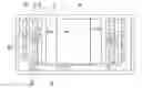
FIG. 1 is a schematic view of the dual VSS wirings in accordance with one embodiment.
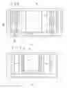
FIG. 2 is a schematic view of the single VSS wirings in accordance with one embodiment.
DETAILED DESCRIPTION OF THE EMBODIMENTS
Embodiments of the invention will now be described more fully hereinafter with reference to the accompanying drawings, in which embodiments of the invention are shown.
FIG. 1 is a schematic view of the dual VSS wirings in accordance with one embodiment.
FIG. 2 is a schematic view of the single VSS wirings in accordance with one embodiment.
In the first embodiment:
An array substrate for enhancing GOA reliability includes a GOA circuit 1, a clock signals (CK) trace 2, a peripheral trace (CF_COM) 3, an active display area (AA) 4, wherein the CF_COM is a testing pad (Pad) lead out from the CF_COM Lead on the COF.
As shown in FIG. 1, the array substrate includes dual and adjacent VSS traces in a rim, wherein VSS is a common negative electrode, which also relates to a voltage serious. The VSS traces include a first VSS trace 5 (VSS1) and a second VSS trace 6 (VSS2), 2n number of regulation capacitors 8 are configured between the CF_COM trace 3 and the second VSS trace 6 (VSS2) via the metal material in different layers, wherein n is a positive integer. An end of the first VS S trace 5 (VSS1) connects with an end of the second VSS trace 6 (VSS2), and a regulation capacitor is configured in a connection location of the first VSS trace 5 (VSS1) and the second VSS trace 6 (VSS2).
The CK trace 2 includes two CK traces 2 arranged at two lateral sides of the active display area (AA) 4. That is, the CK traces 2 are respectively between the first VSS trace 5 (VSS1) and the second VS S trace 6 (VSS2) or arranged in a rim of the GOA circuit 1. The 2n number of regulation capacitors are arranged at the left side and the right side of the active display area (AA) 4 and are symmetrical to each other. One plate layer of the regulation capacitors 8 is made by metallic material different from the VSS trace. The GOA circuit 1 is symmetrical with respect to two lateral sides of the active display area (AA) 4. The array substrate for enhancing the GOA reliability may be adopted in the display panel. The first VSS trace 5 (VSS1), the second VSS trace 6 (VSS2), a third VSS trace 7 (VSS3), and the CF_COM trace 3 are in different planes.
Second Embodiment
The impact caused by the VSS trace will be described hereinafter.
The array substrate for enhancing the GOA reliability includes the GOA circuit 1, the CK trace 2, the CF_COM trace 3, and the active display area 4 (AA).
As shown in FIG. 2, a single third VSS trace 7 (VSS3) is configured between the GOA circuit 1 and the CF_COM trace 3 of the active display area 4 (AA), wherein 2n number of regulation capacitors 8 are configured between the third VSS trace 7 (VSS3) and the CF_COM trace 3 by metallic materials in different layer, wherein n is a positive integer. The third VSS trace 7 (VSS3) is arranged at both sides of the active display area 4 (AA).
The CK trace 2 includes two CK traces 2 arranged at two lateral sides of the active display area (AA) 4. That is, the CK traces 2 are respectively between the first VSS trace 5 (VSS1) and the second VS S trace 6 (VSS2) or arranged in a rim of the GOA circuit 1. The 2n number of regulation capacitors are arranged at the left side and the right side of the active display area (AA) 4 and are symmetrical to each other. One plate layer of the regulation capacitors 8 is made by metallic material different from the VSS trace. The GOA circuit 1 is symmetrical on both sides of the active display area (AA) 4. The array substrate for enhancing the GOA reliability may be adopted in the display panel. The first VSS trace 5 (VSS1), the second VSS trace 6 (VSS2), the third VSS trace 7 (VSS3), and the CF_COM trace 3 are in different planes.
It is believed that the present embodiments and their advantages will be understood from the foregoing description, and it will be apparent that various changes may be made thereto without departing from the spirit and scope of the invention or sacrificing all of its material advantages, the examples hereinbefore described merely being preferred or exemplary embodiments of the invention.
Claims
What is claimed is:1. An array substrate for enhancing gate driver on array (GOA) reliability, comprising:
a GOA circuit, a clock signals (CK) trace, a peripheral trace (CF_COM), an active display area (AA), wherein:
the array substrate comprises dual and adjacent VSS traces in a rim, the VSS traces comprise a first VSS trace and a second VSS trace, 2n number of regulation capacitors are configured between the CF_COM trace and the second VSS trace via metal material in different layers, wherein n is a positive integer.
2. An array substrate for enhancing gate driver on array (GOA) reliability, comprising:
a GOA circuit, a clock signals (CK) trace, a peripheral trace (CF_COM), an active display area (AA), wherein:
a single third VSS trace is configured between the GOA circuit and the CF_COM in the active display area (AA), 2n number of regulation capacitors are configured between the CF_COM trace and the third VSS trace via metal material in different layers, wherein n is a positive integer.
3. The array substrate as claimed in claim 1, wherein an end of the first VSS trace connects with an end of the second VSS trace.
4. The array substrate as claimed in claim 3, wherein the CK trace comprises two CK traces arranged at two lateral sides of the active display area (AA), and the CK traces are respectively between the first VSS trace and the second VSS trace or arranged in a rim of the GOA circuit.
5. The array substrate as claimed in claim 2, wherein the third VSS trace is respectively arranged at two lateral sides of the active display area (AA).
6. The array substrate as claimed in claim 1, wherein 2n number of regulation capacitors are arranged at the two lateral sides of the active display area (AA) and are symmetrical to each other.
7. The array substrate as claimed in claim 2, wherein 2n number of regulation capacitors are arranged at the two lateral sides of the active display area (AA) and are symmetrical to each other.
8. The array substrate as claimed in claim 1, wherein the GOA circuit is symmetrical with respect to two lateral sides of the active display area.
9. The array substrate as claimed in claim 2, wherein the GOA circuit is symmetrical with respect to two lateral sides of the active display area.
10. The array substrate as claimed in claim 1, wherein a regulation capacitor is configured in a connection location of the first VSS trace and the second VSS trace.
11. The array substrate as claimed in claim 1, wherein the array substrate is adopted in a display panel.
12. The array substrate as claimed in claim 1, wherein the first VSS trace, the second VSS trace, and the CF_COM trace are in different planes.
13. The array substrate as claimed in claim 2, wherein the first VSS trace, the second VSS trace, the third VSS trace, and the CF_COM trace are in different planes.
Images & Drawings included:
Sources:
- United States Patent and Trademark Office - verify current appl. status at the USPTO↗
Recent applications in this class:
- » 20250292740 2025-09-18
DISPLAY DEVICE - » 20240194155 2024-06-13
DISPLAY DEVICE - » 20230147567 2023-05-11
Display device - » 20220068227 2022-03-03
Power monitoring for correcting ambient temperature measurement by electronic devices - » 20210027721 2021-01-28
Display apparatus and method thereof - » 20200211478 2020-07-02
DISPLAY APPARATUS FOR EYE STRAIN REDUCTION - » 20200126493 2020-04-23
Blue light compensation film and OLED display - » 20200126492 2020-04-23
Blue light compensation film and OLED display - » 20200126491 2020-04-23
Blue light compensation film and OLED display - » 20200126490 2020-04-23
Blue light compensation film and OLED display
Recent applications for this Assignee:
- » 20200355948 2020-11-12
FRAME SEALANT AND LIQUID CRYSTAL DISPLAY PANEL - » 20200341310 2020-10-29
Thin film transistor liquid crystal display (TFT-LCD) and the driving circuit and switching power supply thereof - » 20200285088 2020-09-10
Array substrate of thin-film transistor liquid crystal display device and method for manufacturing the same - » 20200272004 2020-08-27
Array substrate and liquid crystal display panel - » 20200258866 2020-08-13
Display panel, manufacturing method thereof and display device - » 20200251055 2020-08-06
Brightness regulation device of display device, brightness regulation method and display device - » 20200201464 2020-06-25
Array substrate and touch display device - » 20200185452 2020-06-11
Manufacturing method of micro light-emitting diode display panel - » 20200181759 2020-06-11
VAPOR DEPOSITION CRUCIBLE - » 20200168842 2020-05-28
Organic light-emitting diode (OLED) display panel and manufacturing method thereof