Reference voltage circuit including depletion type and enhancement type transistors in a common centroid arrangement
US20180348807A1
2018-12-06
15/994,075
2018-05-31
✅ Patent granted
US 11,275,399 B2
2022-03-15
-
-
Thienvu V Tran | Nusrat Quddus
Crowell & Moring LLP
2039-08-06
Abstract:
There is provided a reference voltage circuit which includes a depletion type transistor and an enhancement type transistor. At least one of the depletion type transistor and the enhancement type transistor is formed from a plurality of transistors and the reference voltage circuit is arranged in the form of a common centroid (common center of mass) to avoid the influence of a characteristic fluctuation due to stress from the resin encapsulation of a semiconductor device or the like.
Inventors:
- Masakazu SUGIURA 46 🇯🇵 Chiba, Japan
- Masakazu SUGIURA 53 🇯🇵 Chiba-shi, Japan
- Fumihiko MAETANI 24 🇯🇵 Chiba-shi, Japan
- Fumihiko Maetani 21 🇯🇵 Chiba, Japan
Assignee:
- ABLIC Inc. 211 🇯🇵 Chiba, Japan
Applicant:
Interested in similar patents?
Get notified when new applications in this technology area are published.
Classification:
H01L27/088 IPC
Devices consisting of a plurality of semiconductor or other solid-state components formed in or on a common substrate including semiconductor components specially adapted for rectifying, oscillating, amplifying or switching and having at least one potential-jump barrier or surface barrier; including integrated passive circuit elements with at least one potential-jump barrier or surface barrier the substrate being a semiconductor body including only semiconductor components of a single kind including field-effect components only the components being field-effect transistors with insulated gate
G05F3/26 IPC
Regulating voltage or current wherein the variable is dc using uncontrolled devices with non-linear characteristics being semiconductor devices using diode- transistor combinations Current mirrors
G05F3/262 » CPC main
Regulating voltage or current wherein the variable is dc using uncontrolled devices with non-linear characteristics being semiconductor devices using diode- transistor combinations; Current mirrors using field-effect transistors only
H01L27/0883 » CPC further
Devices consisting of a plurality of semiconductor or other solid-state components formed in or on a common substrate including semiconductor components specially adapted for rectifying, oscillating, amplifying or switching and having at least one potential-jump barrier or surface barrier; including integrated passive circuit elements with at least one potential-jump barrier or surface barrier the substrate being a semiconductor body including only semiconductor components of a single kind including field-effect components only the components being field-effect transistors with insulated gate Combination of depletion and enhancement field effect transistors
Description
RELATED APPLICATIONS
This application claims priority under 35 U.S.C. § 119 to Japanese Patent Application Nos. 2017-109043 filed Jun. 1, 2017 and 2018-060317 filed Mar. 27, 2018, the entire content of which are hereby incorporated by reference.
BACKGROUND OF THE INVENTION
Field of the Invention
The present invention relates to a reference voltage circuit and a semiconductor device.
Background Art
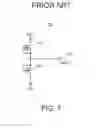
There has been known as a reference voltage circuit, a reference voltage circuit 700 in which such depletion type and enhancement type transistors as illustrated in FIG. 7 are combined (refer to, for example, Japanese Unexamined Patent Application Publication No. 2012-531825).
The reference voltage circuit 700 is equipped with a depletion type transistor 710, an enhancement type transistor 720, and a terminal 730 which outputs a reference voltage VREF.
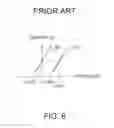
The operation of the reference voltage circuit 700 will be described with reference to FIG. 8. The threshold voltage of the transistor 710 is VTND, and the relationship between the voltage and the current of the transistor 710 is shown as a curve 801. The threshold voltage of the transistor 720 is VTNE, and the relationship between the voltage and the current of the transistor 720 is shown as a curve 802. A voltage generated by making a current based on the value of the intercept of the curve 801 flow into the enhancement type transistor 720 is output to the terminal 730 as the reference voltage VREF.
SUMMARY OF THE INVENTION
It has generally been known that a semiconductor device causes a characteristic variation with the influence of stress due to its resin encapsulation (packaging).
For example, when stress is applied in an x-axis direction where a semiconductor device having the transistors 710 and 720 arranged in the x-axis direction is resin-encapsulated, there is a possibility that the characteristic fluctuations of the transistors 710 and 720 will deviate. That is, the curves 801 and 802 respectively have a possibility of deviating from a desired characteristic.
The present invention has been made to avoid the influence of a characteristic fluctuation due to stress in the resin encapsulation of a semiconductor device or the like and provides a semiconductor device equipped with a reference voltage circuit with less product variation.
There is provided a reference voltage circuit of the present invention, in which a depletion type transistor or/and an enhancement type transistor are respectively configured of a plurality of transistors and arranged in the form of a common centroid (common center of mass).
According to the reference voltage circuit of the present invention, it is possible to provide a semiconductor device equipped with a reference voltage circuit which avoids the influence of a characteristic fluctuation due to stress in the resin encapsulation of the semiconductor device or the like and provides less product variation.
BRIEF DESCRIPTION OF THE DRAWINGS
FIG. 1 is an explanatory diagram illustrating a reference voltage circuit according to a first embodiment of the present invention;
FIG. 2 is an explanatory diagram illustrating another example of the reference voltage circuit according to the first embodiment;
FIG. 3 is an explanatory diagram illustrating a further example of the reference voltage circuit according to the first embodiment;
FIG. 4 is an explanatory diagram illustrating yet another example of the reference voltage circuit according to the first embodiment;
FIG. 5 is an explanatory diagram illustrating a still further example of the reference voltage circuit according to the first embodiment;
FIG. 6 is an explanatory diagram illustrating a reference voltage circuit according to a second embodiment of the present invention;
FIG. 7 is a circuit diagram illustrating a general reference voltage circuit; and
FIG. 8 is an operation explanatory diagram of the reference voltage circuit illustrated in FIG. 7.
DETAILED DESCRIPTION OF THE EMBODIMENTS
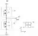
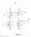
FIG. 1 is an explanatory diagram illustrating a reference voltage circuit according to a first embodiment of the present invention.
The reference voltage circuit 100 is equipped with a depletion type transistor 110, an enhancement type transistor 120, and a terminal 130 which outputs a reference voltage VREF.
The transistor 110 is configured to connect two depletion type transistors 111 and 112 in series. The transistor 120 is configured to connect two transistors 121 and 122 in series.
The reference voltage circuit 100 is similar in operation to a general reference voltage circuit comprised of a depletion type transistor 110 and an enhancement type transistor 120 and outputs the reference voltage VREF to the terminal 130.
Here, the reference voltage circuit 100 is configured to set the transistors 111 and 112 to be the same size (W length and L length) and set the transistors 121 and 122 to be the same size (W length and L length). Then, the transistors 111, 112, 121, and 122 are arranged on a semiconductor device approximately in the form of a common centroid (common center of mass) as illustrated in FIG. 1.
That is, the transistor pair 111 and 112, and the transistor pair 121 and 122 are arranged point-symmetrically to have respective center of mass at substantially the same position to realize the common centroid (common center of mass).
In the reference voltage circuit 100 arranged as described above, even if the characteristics of the transistors change in an x-axis or y-axis direction due to stress in resin encapsulation or the like, the transistor 110 and the transistor 120 are subjected to the same influence. Thus, there is brought about an advantageous effect that since the transistors 110 and 120 cause the same characteristic variation, it is possible to reduce a deviation of its variation characteristic from a desired voltage/current characteristic.
As described above, since the transistor 110 and the transistor 120 are arranged on the semiconductor device approximately in the form of the common centroid in the reference voltage circuit 100, it is possible to provide a semiconductor device equipped with a reference voltage circuit which avoids the influence of a characteristic fluctuation due to the stress in the resin encapsulation of the semiconductor device or the like and provides less product variation.
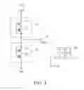
FIG. 2 is an explanatory diagram illustrating another example of the reference voltage circuit according to the first embodiment.
The reference voltage circuit 200 includes a depletion type transistor 210 and an enhancement type transistor 220 respectively configured from three transistors.
The transistor 210 is configured from three depletion type transistors 211, 212, and 213 connected in series. The transistor 220 is configured from three transistors 221, 222, and 223 connected in series.
Here, the respective transistors are configured as with the reference voltage circuit 100 and arranged on a semiconductor device approximately in the form of a common centroid (common center of mass) as illustrated in FIG. 2. The reference voltage circuit 200 configured in this manner is also capable of obtaining a similar effect.
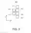
Further, the reference voltage circuit 200 may be arranged on a semiconductor device approximately in the form of a common centroid (common center of mass) as illustrated in FIG. 3. That is, the transistors 211, 212, and 223, and the transistors 213, 221, and 222 are arranged in linear symmetry to realize the common centroid (common center of mass).
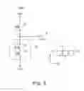
FIG. 4 is an explanatory diagram illustrating yet another example of the reference voltage circuit according to the first embodiment.
The reference voltage circuit 400 includes a depletion type transistor 410 and an enhancement type transistor 420 respectively configured from two transistors.
The transistor 410 is configured from two depletion type transistors 411 and 412 connected in parallel. The transistor 420 is configured from two transistors 421 and 422 connected in parallel.
As with the reference voltage circuit 100 illustrated in FIG. 1, the reference voltage circuit 400 is arranged on a semiconductor device approximately in the form of a common centroid (common center of mass). The reference voltage circuit 400 configured in this manner is also capable of obtaining a similar effect.
Incidentally, although the reference voltage circuit 400 includes the transistors respectively configured to connect the two transistors in parallel, more than two may be connected in parallel and arranged on a semiconductor device approximately in the form of a common centroid (common center of mass).
FIG. 5 is an explanatory diagram illustrating a still further example of the reference voltage circuit according to the first embodiment.
The reference voltage circuit 500 is equipped with a depletion type transistor 110, an enhancement type transistor 120, and a terminal 130 which outputs a reference voltage VREF. The transistor 120 is configured from two transistors 121 and 122 connected in series.
Although the depletion type transistor 110 is configured from the two depletion type transistors 111 and 112 connected in series in the reference voltage circuit 100 of FIG. 1, the depletion type transistor 110 can be arranged on a semiconductor device approximately in the form of a common centroid (common center of mass) even if the depletion type transistor 110 is formed from one transistor as illustrated in FIG. 5.
Incidentally, although there has been described the example in which the depletion type transistor 110 is comprised of one transistor in the reference voltage circuit 500 in FIG. 5, the enhancement type transistor 120 may be comprised of one transistor.
Although the above-described reference voltage circuit according to the first embodiment includes the transistors respectively configured from one to three transistors, more than three may be connected in series or parallel and arranged on the semiconductor device approximately in the form of the common centroid (common center of mass).
FIG. 6 is an explanatory diagram illustrating a reference voltage circuit according to a second embodiment of the present invention.
The reference voltage circuit 600 has a depletion type transistor 610, an enhancement type transistor 620, and transistors 640 and 650 which form a current mirror circuit. The reference voltage circuit 600 is configured by coupling the transistors 610 and 620 with the current mirror circuit and is similar in basic operation to the reference voltage circuit according to the first embodiment. The reference voltage circuit 600 is formed from a plurality of transistors as with the reference voltage circuit according to the first embodiment.
The transistor 610 is configured from two depletion type transistors 611 and 612 connected in series. The transistor 620 is configured from two transistors 621 and 622 connected in series. The transistor 640 is configured from two transistors 641 and 642 connected in series. The transistor 650 is configured from two transistors 651 and 652 connected in series.
The respective transistors are configured as with those in the reference voltage circuit according to the first embodiment. Further, as with the reference voltage circuit 100, for example, the transistors 610 and 620 are arranged on a semiconductor device approximately in the form of a common centroid (common center of mass), and the transistors 640 and 650 are arranged on the semiconductor device approximately in the form of the common centroid (common center of mass). The reference voltage circuit 600 configured in this manner is also capable of obtaining a similar effect.
Incidentally, although the reference voltage circuit 600 according to the second embodiment includes the transistors respectively configured from the two transistors, more than two may be connected in series or parallel as with the first embodiment and arranged on the semiconductor device approximately in the form of the common centroid (common center of mass).
Claims
What is claimed is:1. A reference voltage circuit comprising:
a depletion type transistor which is a current source; and
an enhancement type transistor which is a load,
at least one of the depletion type transistor and the enhancement type transistor being comprised of a plurality of transistors, and
the depletion type transistor and the enhancement type transistor being arranged in the form of a common centroid (common center of mass).
2. The reference voltage circuit according to claim 1, wherein the depletion type transistor and the enhancement type transistor are arranged point-symmetrically.
3. The reference voltage circuit according to claim 1, wherein the depletion type transistor and the enhancement type transistor are arranged in linear symmetry.
4. The reference voltage circuit according to claim 1, wherein the depletion type transistor and the enhancement type transistor are connected through a current mirror circuit.
5. The reference voltage circuit according to claim 2, wherein the depletion type transistor and the enhancement type transistor are connected through a current mirror circuit.
6. The reference voltage circuit according to claim 3, wherein the depletion type transistor and the enhancement type transistor are connected through a current mirror circuit.
7. The reference voltage circuit according to claim 4, wherein each transistor configuring the current mirror circuit is comprised of a plurality of transistors, and
wherein the plurality of transistors are arranged in the form of a common centroid (common center of mass).
8. The reference voltage circuit according to claim 5, wherein each transistor configuring the current mirror circuit is comprised of a plurality of transistors, and
wherein the plurality of transistors are arranged in the form of a common centroid (common center of mass).
9. The reference voltage circuit according to claim 6, wherein each transistor configuring the current mirror circuit is comprised of a plurality of transistors, and
wherein the plurality of transistors are arranged in the form of a common centroid (common center of mass).
10. A semiconductor device comprising a reference voltage circuit according to claim 1.
11. A semiconductor device comprising a reference voltage circuit according to claim 2.
12. A semiconductor device comprising a reference voltage circuit according to claim 3.
13. A semiconductor device comprising a reference voltage circuit according to claim 4.
14. A semiconductor device comprising a reference voltage circuit according to claim 5.
Images & Drawings included:


Sources:
- United States Patent and Trademark Office - verify current appl. status at the USPTO↗
Recent applications in this class:
- » 20250291377 2025-09-18
CIRCUIT AND SYSTEM FOR ACTIVELY DISCHARGING A POWER STAGE INPUT NODE DURING POWER SUPPLY TURN-ON - » 20250284306 2025-09-11
Bias Circuit and the Control Method thereof - » 20250284305 2025-09-11
VOLTAGE REFERENCE CIRCUIT USING FIELD-EFFECT TRANSISTORS - » 20250271889 2025-08-28
Leakage Insensitive Switch Control for Bandgap Thermal Sensors in Core-MOS Nodes - » 20250264901 2025-08-21
FAST POWER-UP SCHEME FOR CURRENT MIRRORS - » 20250264900 2025-08-21
LOW VOLTAGE CASCODE CURRENT MIRROR - » 20250264899 2025-08-21
BIASING CIRCUIT - » 20250251749 2025-08-07
Controllable Temperature Coefficient Bias Circuit - » 20250224752 2025-07-10
Bandgap Circuit Having A Base Current Redistribution Circuit - » 20250216884 2025-07-03
REFERENCE CURRENT GENERATING CIRCUIT AND ASSOCIATED CALIBRATION METHOD
Recent applications for this Assignee:
- » 20210389386 2021-12-16
Semiconductor device - » 20200379492 2020-12-03
Voltage regulator having a phase compensation circuit - » 20200366201 2020-11-19
Transmission circuit for transmitting signals - » 20200350398 2020-11-05
Semiconductor device and method of manufacturing the same - » 20200313081 2020-10-01
Semiconductor device - » 20200313080 2020-10-01
Semiconductor device - » 20200313079 2020-10-01
Semiconductor device - » 20200312993 2020-10-01
Semiconductor device and manufacturing method thereof - » 20200309868 2020-10-01
Magnetic substance detection sensor - » 20200295124 2020-09-17
Semiconductor device and method of manufacturing the same