Thermally activated delayed fluorescence material and application thereof in organic electroluminescence device
US20190074447A1
2019-03-07
15/770,730
2016-11-30
✅ Patent granted
US 10,770,661 B2
2020-09-08
WO; PCT/CN2016/107913; 20161130
WO; WO2017/101675; 20170622
Deepak R Rao
Maschoff Brennan
2037-01-05
Abstract:
The present invention discloses a thermally activated delayed fluorescence material and application thereof in an organic electroluminescence device. The thermally activated delayed fluorescence material is a compound having the general structure of Formula I or Formula II:
In Formula I and Formula II, R1 is a cyano, p is 1, 2 or 3, q is 1, 2 or 3, m is 1 or 2, n is 1 or 2,
- Ar1 is a phenyl substituted with one or more groups selected from C1-6 alkyl, methoxy, ethoxy, or phenyl,
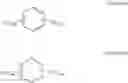
- Ar2 and Ar3 are selected from the following groups:
and X is bromine or iodine. The present invention further discloses application of the thermally activated delayed fluorescence material as a host material or a luminescent dye of a luminescent layer of an organic electroluminescence device.
Inventors:
- Song LIU 72 🇨🇳 Beijing, China
- Lian DUAN 24 🇨🇳 Beijing, China
- Dongdong ZHANG 55 🇨🇳 Beijing, China
- Fei ZHAO 24 🇨🇳 Beijing, China
Assignee:
- Tsinghua University 3,118 🇨🇳 Beijing, China
- KUNSHAN GO-VISIONOX OPTO-ELECTRONICS CO., LTD. 2 🇨🇳 KunShan City, Jiangsu, China
- KUNSHAN GP-VISIONOX OPTO-ELECTRONICS CO., LTD. 1 🇨🇳 Kunshan, China
Applicant:
Interested in similar patents?
Get notified when new applications in this technology area are published.
Classification:
C07D241/48 » CPC further
Heterocyclic compounds containing 1,4-diazine or hydrogenated 1,4-diazine rings condensed with carbocyclic rings or ring systems with only hydrogen or carbon atoms directly attached to the ring nitrogen atoms; Phenazines with hydrocarbon radicals, substituted by nitrogen atoms, directly attached to the ring nitrogen atoms
C07D265/38 » CPC further
Heterocyclic compounds containing six-membered rings having one nitrogen atom and one oxygen atom as the only ring hetero atoms 1,4-Oxazines; Hydrogenated 1,4-oxazines condensed with carbocyclic rings [b, e]-condensed with two six-membered rings
C07D279/28 » CPC further
Heterocyclic compounds containing six-membered rings having one nitrogen atom and one sulfur atom as the only ring hetero atoms 1,4-Thiazines; Hydrogenated 1,4-thiazines condensed with carbocyclic rings or ring systems [b, e]-condensed with two six-membered rings with carbon atoms directly attached to the ring nitrogen atom with hydrocarbon radicals, substituted by amino radicals, attached to the ring nitrogen atom with other substituents attached to the ring system
C07D209/88 » CPC further
Heterocyclic compounds containing five-membered rings, condensed with other rings, with one nitrogen atom as the only ring hetero atom; Ring systems containing three or more rings [b, c]- or [b, d]-condensed; Carbazoles; Hydrogenated carbazoles with hetero atoms or with carbon atoms having three bonds to hetero atoms with at the most one bond to halogen, e.g. ester or nitrile radicals, directly attached to carbon atoms of the ring system
C09K11/06 » CPC further
Luminescent, e.g. electroluminescent, chemiluminescent materials containing organic luminescent materials
C07D487/04 » CPC further
Heterocyclic compounds containing nitrogen atoms as the only ring hetero atoms in the condensed system, not provided for by groups - in which the condensed system contains two hetero rings Ortho-condensed systems
H01L51/0059 » CPC further
Solid state devices using organic materials as the active part, or using a combination of organic materials with other materials as the active part; Processes or apparatus specially adapted for the manufacture or treatment of such devices, or of parts thereof; Selection of organic semiconducting materials, e.g. organic light sensitive or organic light emitting materials; Macromolecular systems with low molecular weight, e.g. cyanine dyes, coumarine dyes, tetrathiafulvalene Amine compounds having at least two aryl rest on at least one amine-nitrogen atom, e.g. triphenylamine
C07D251/24 » CPC further
Heterocyclic compounds containing 1,3,5-triazine rings not condensed with other rings having three double bonds between ring members or between ring members and non-ring members with hydrogen or carbon atoms directly attached to at least one ring carbon atom to three ring carbon atoms
C07D403/14 » CPC further
Heterocyclic compounds containing two or more hetero rings, having nitrogen atoms as the only ring hetero atoms, not provided for by group containing three or more hetero rings
C07D417/14 » CPC further
Heterocyclic compounds containing two or more hetero rings, at least one ring having nitrogen and sulfur atoms as the only ring hetero atoms, not provided for by group containing three or more hetero rings
H01L51/0072 » CPC main
Solid state devices using organic materials as the active part, or using a combination of organic materials with other materials as the active part; Processes or apparatus specially adapted for the manufacture or treatment of such devices, or of parts thereof; Selection of organic semiconducting materials, e.g. organic light sensitive or organic light emitting materials; Macromolecular systems with low molecular weight, e.g. cyanine dyes, coumarine dyes, tetrathiafulvalene aromatic compounds comprising a hetero atom, e.g.: N,P,S; Polycyclic condensed heteroaromatic hydrocarbons comprising only nitrogen in the heteroaromatic polycondensed ringsystem, e.g. phenanthroline, carbazole
H01L51/0067 » CPC further
Solid state devices using organic materials as the active part, or using a combination of organic materials with other materials as the active part; Processes or apparatus specially adapted for the manufacture or treatment of such devices, or of parts thereof; Selection of organic semiconducting materials, e.g. organic light sensitive or organic light emitting materials; Macromolecular systems with low molecular weight, e.g. cyanine dyes, coumarine dyes, tetrathiafulvalene aromatic compounds comprising a hetero atom, e.g.: N,P,S comprising only nitrogen as heteroatom
H01L51/00 IPC
Solid state devices using organic materials as the active part, or using a combination of organic materials with other materials as the active part; Processes or apparatus specially adapted for the manufacture or treatment of such devices, or of parts thereof
H01L51/5012 » CPC further
Solid state devices using organic materials as the active part, or using a combination of organic materials with other materials as the active part; Processes or apparatus specially adapted for the manufacture or treatment of such devices, or of parts thereof specially adapted for light emission, e.g. organic light emitting diodes [OLED] or polymer light emitting devices [PLED] Electroluminescent [EL] layer
H01L51/5056 » CPC further
Solid state devices using organic materials as the active part, or using a combination of organic materials with other materials as the active part; Processes or apparatus specially adapted for the manufacture or treatment of such devices, or of parts thereof specially adapted for light emission, e.g. organic light emitting diodes [OLED] or polymer light emitting devices [PLED]; Carrier transporting layer Hole transporting layer
H01L51/5072 » CPC further
Solid state devices using organic materials as the active part, or using a combination of organic materials with other materials as the active part; Processes or apparatus specially adapted for the manufacture or treatment of such devices, or of parts thereof specially adapted for light emission, e.g. organic light emitting diodes [OLED] or polymer light emitting devices [PLED]; Carrier transporting layer Electron transporting layer
H01L51/5088 » CPC further
Solid state devices using organic materials as the active part, or using a combination of organic materials with other materials as the active part; Processes or apparatus specially adapted for the manufacture or treatment of such devices, or of parts thereof specially adapted for light emission, e.g. organic light emitting diodes [OLED] or polymer light emitting devices [PLED] Carrier injection layer
C07D413/14 » CPC further
Heterocyclic compounds containing two or more hetero rings, at least one ring having nitrogen and oxygen atoms as the only ring hetero atoms containing three or more hetero rings
C07D403/10 » CPC further
Heterocyclic compounds containing two or more hetero rings, having nitrogen atoms as the only ring hetero atoms, not provided for by group containing two hetero rings linked by a carbon chain containing aromatic rings
H01L51/50 » CPC further
Solid state devices using organic materials as the active part, or using a combination of organic materials with other materials as the active part; Processes or apparatus specially adapted for the manufacture or treatment of such devices, or of parts thereof specially adapted for light emission, e.g. organic light emitting diodes [OLED] or polymer light emitting devices [PLED]
Description
TECHNICAL FIELD
The present invention belongs to the field of materials, and particularly relates to a thermally activated delayed fluorescence material and application thereof in an organic electroluminescence device.
BACKGROUND ART
In the electroluminescence process of an organic electroluminescence device, luminescence occurs mainly due to the electronic transition of an organic luminescent material from an excited state to a ground state. At room temperature, luminescence generated by the electronic transition from a triplet excited state back to the ground state is extremely weak, most of the energy is lost in the form of heat, and luminescence is mainly generated by the electronic transition from a singlet excitation state to the ground state, and is called electroluminescence. Since the probability of the triplet excited state is three times that of the singlet excitation state, the equivalent of 75% of the energy is not used for luminescence. Making full use of the energy will effectively improve the luminescence efficiency of the organic electroluminescence device.
In order to make full use of the energy of the triplet excited state of a host material of a luminescent layer, various methods have been proposed. For example, by researching and developing an efficient phosphorescence doping dye and doping the phosphorescence doping dye into the host material, the triplet energy of the host material can be effectively transmitted to the phosphorescence doping dye, and then the phosphorescence doping dye generates phosphorescence, thereby allowing the energy of the triplet excited state of the host material of the luminescent layer to be effectively used. The organic electroluminescence device obtained by this method has high efficiency, but material synthesis requires precious metals such as ruthenium and platinum which are expensive. Another method is to utilize the intersystem crossing property of lanthanide compounds, namely intramolecular energy transfer, to transfer the triplet energy of the host material of the luminescent layer to the 4f energy level of lanthanide metal ions, and then luminescence and the like are achieved, but current devices are inefficient.
Thermally activated delayed fluorescence (TADF) is a quite popular scheme utilizing triplet exciton energy at present. For example, Adachi reported in his article a thermally activated delayed fluorescence material which has a small difference (ΔEST) between the triplet energy level (T1) and the singlet energy level (S1), in this way, triplet energy can be transmitted to the singlet energy level, and light is emitted through fluorescent radiation. Patent CN 102709485 A mentions that device efficiency is improved by doping a fluorescent dye in a thermal delay fluorescent host. In order to further improve energy transmission recombination efficiency, in the article “High-efficiency organic light-emitting diodes with fluorescent emitters” by Adachi et al. in Nature communications 2014, a wide-band-gap host doped TADF material is proposed as an auxiliary dye solution. However, in the process of charge recombination, part of the energy is directly compounded on a host, the host transmits the singlet energy to a dye, and the other part is compounded on an auxiliary dye. The structure reported in the article can not fully and effectively utilize the energy directly compounded on the host. At the same time, an ordinary host material is used, a band gap is wide, and required driving voltage is high.
However, the current TADF material has a short lifetime, and one of the reasons is that the lifetime of the triplet state is too long, and exciton quenching can be caused easily due to processes such as TPA. Therefore, the lifetime of a TADF device can be effectively increased by reducing the lifetime of triplet excitons.
Technical Problems
The technical problem to be solved by the present invention is that a TADF material in the prior art has a short lifetime.
Technical Solution
In order to solve the above technical problem, the present invention provides a novel TADF material. By introducing heavy atoms such as bromine or iodine into original TADF molecules, reverse intersystem crossing and intersystem crossing of the TADF material can be increased through the heavy atom effect, so that the lifetime of triplet excitons can be reduced, and ultimately the lifetime of a device can be increased.
The thermally activated delayed fluorescence material provided by the present invention is a compound having the general structure of Formula I or Formula II:
In Formula I and Formula II, R1 is a cyano, p is 1, 2 or 3, q is 1, 2 or 3, m is 1 or 2, n is 1 or 2,
Ar1 is a phenyl substituted with one or more groups selected from C1-6 alkyl, methoxy, ethoxy, or phenyl,
Ar2 and Ar3 are selected from the following groups:
and X is bromine or iodine.
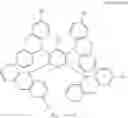
Preferably, the thermally activated delayed fluorescence material is a compound having the following structure:
The present invention also provides application of the thermally activated delayed fluorescence material as a host material or a luminescent dye of a luminescent layer of an organic electroluminescence device.
The present invention further provides an organic electroluminescence device, comprising a luminescent layer, the luminescent layer comprises a host material and a luminescent dye doped in the host material, and the luminescent dye is the above thermally activated delayed fluorescence material. Preferably, the luminescent dye accounts for 0.5 wt %-10 wt % of the luminescent layer, and more preferably 5 wt %.
As a preferred technical solution, the organic electroluminescence device described above comprises an anode, a hole transport layer, a luminescent layer, an electron transport layer, and a cathode, which are successively deposited on a substrate and are laminated.
Preferably, a hole injection layer is further disposed between the anode and the hole transport layer.
The present invention further provides an organic electroluminescence device, comprising a luminescent layer, the luminescent layer comprises a host material and a luminescent dye doped in the host material, and the host material is the above thermally activated delayed fluorescence material.
Preferably, the luminescent dye accounts for 1 wt %-10 wt % of the luminescent layer.
Advantageous Effects
According to the TADF material provided by the invention, by introducing heavy atoms such as bromine or iodine into molecules, the lifetime of the triplet state of the TADF material is reduced, and efficiency roll-off is reduced, thereby increasing the lifetime of the organic electroluminescence device.
BRIEF DESCRIPTION OF THE DRAWINGS
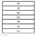
FIG. 1 is the schematic diagram of the structure of an organic electroluminescence device of the present invention.
PREFERRED EMBODIMENTS OF THE INVENTION
The present invention will be further illustrated below by referring to the drawings and the special examples, to enable a person skilled in the art to better understand and implement the present invention, but the examples are not taken as limiting the present invention.
A thermally activated delayed fluorescence material provided in the invention is a compound having the general structure of Formula I or Formula II:
In Formula I and Formula II, R1 is a cyano, p is 1, 2 or 3, q is 1, 2 or 3, m is 1 or 2, n is 1 or 2,
Ar1 is a phenyl substituted with one or more groups selected from C1-6 alkyl, methoxy, ethoxy, or phenyl,
Ar2 and Ar3 are selected from the following groups:
and X is bromine or iodine.
According to the thermally activated delayed fluorescence material, by introducing heavy atoms such as bromine or iodine into original TADF molecules, reverse intersystem crossing and intersystem crossing of the TADF material can be increased through the heavy atom effect, so that the lifetime of triplet excitons can be reduced, and ultimately the lifetime of a device can be increased.
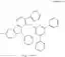
Specifically, the thermally activated delayed fluorescence material of the present invention is compounds having the following structures, and properties and preparation methods of the compounds are as follows:
Preparation Method:
Synthesis of the compound having the structure represented by Formula (1-1): in the nitrogen range, 3-bromocarbazole (5 mmol) is dissolved in 2 mL of anhydrous THF, then sodium hydride (5 mmol) is added, and the mixture is stirred at room temperature for 30 minutes; subsequently, 1,2-dicyano-4,5-difluorobenzene (1 mmol) is added to a reaction flask and stirring is continued for 1 hour; finally, 2 mL of cold water is added to the mixture to quench the reaction. After the mixture is cooled to room temperature, a product of Formula (1-1) is purified by vacuum filtration followed by column chromatography, and the product is dried in vacuum. Yield: 75%.
Molecular weight obtained through mass spectrometry: 615.97.
Relative molecular mass percentage of each element obtained through elemental analysis: C: 62.36; H: 2.62; N: 9.09; Br: 25.93.
Preparation Method:
Synthesis of the compound having the structure represented by Formula (1-2): in the nitrogen range, 3-bromophenothiazine (10 mmol) is dissolved in 4 mL of anhydrous THF, then sodium hydride (10 mmol) is added, and the mixture is stirred at room temperature for 30 minutes; subsequently, 2,3,5,6-tetrafluoro nitrile benzene (1 mmol) is added to a reaction flask and stirring is continued for 1 hour; finally, 2 mL of cold water is added to the mixture to quench the reaction. After the mixture is cooled to room temperature, a product of Formula (1-2) is purified by vacuum filtration followed by column chromatography, and the product is dried in vacuum. Yield: 62%.
Molecular weight obtained through mass spectrometry: 1206.80.
Relative molecular mass percentage of each element obtained through elemental analysis: C: 54.70; H: 2.42; N: 5.80; S: 10.62; Br: 26.46.
Preparation Method:
Synthesis of the compound having the structure represented by Formula (1-3): the reactant 3-bromophenothiazine is replaced with 3-bromophenoxazine, the compound having the structure represented by Formula (1-3) is obtained by a synthesis method which is the same as that of Formula (1-2), and yield is 59%.
Molecular weight obtained through mass spectrometry: 1142.89.
Relative molecular mass percentage of each element obtained through elemental analysis: C: 57.77; H: 2.56; N: 6.12; O: 5.60; Br: 27.95.
Preparation Method:
Synthesis of the compound having the structure represented by Formula (1-4): the reactant 3-bromophenothiazine is replaced with 9-p-iodobenzene phenazine, the compound having the structure represented by Formula (1-4) is obtained by a synthesis method which is the same as that of Formula (1-2), and yield is 55%.
Molecular weight obtained through mass spectrometry: 1631.03.
Relative molecular mass percentage of each element obtained through elemental analysis: C: 58.14; H: 3.03; N: 7.72; I: 31.11.
Preparation Method:
Synthesis of the compound having the structure represented by Formula (1-5): in the nitrogen range, (1,1′-p-dibromobenzene) p-aminobenzene (15 mmol) is dissolved in 6 mL of anhydrous THF, then sodium hydride (15 mmol) is added, and the mixture is stirred at room temperature for 30 minutes; subsequently, 2,4,6-tetrafluoro-1,3,5-tricyanobenzene (1 mmol) is added to a reaction flask and stirring is continued for 1 hour; finally, 2 mL of cold water is added to the mixture to quench the reaction. After the mixture is cooled to room temperature, a product of Formula (1-5) is purified by vacuum filtration followed by column chromatography, and the product is dried in vacuum. Yield: 31%.
Molecular weight obtained through mass spectrometry: 1355.80.
Relative molecular mass percentage of each element obtained through elemental analysis: C: 55.78; H: 2.68; N: 6.20; Br: 35.34.
Preparation Method:
Synthesis of the compound having the structure represented by Formula (2-1): in the nitrogen range, 3,6-dibromocarbazolylbenzene (10 mmol) is dissolved in 4 mL of anhydrous THF, then sodium hydride (15 mmol) is added, and the mixture is stirred at room temperature for 30 minutes; subsequently, 1-phenyl-1,3,5-triazine (1 mmol) is added to a reaction flask and stirring is continued for 1 hour; finally, 2 mL of cold water is added to the mixture to quench the reaction. After the mixture is cooled to room temperature, a product of Formula (2-1) is purified by vacuum filtration followed by column chromatography, and the product is dried in vacuum. Yield: 49%.
Molecular weight obtained through mass spectrometry: 955.33.
Relative molecular mass percentage of each element obtained through elemental analysis: C: 56.58; H: 2.64; N: 7.33; Br: 33.46.
Preparation Method:
Synthesis of the compound having the structure represented by Formula (2-2): in the nitrogen range, p-bromobenzene (5 mmol) is dissolved in 4 mL of anhydrous THF, then sodium hydride (5 mmol) is added, and the mixture is stirred at room temperature for 30 minutes; subsequently, 2,4-bis(3-bicarbazole)-6-fluoro-1,3,5-triazine (1 mmol) is added to a reaction flask and stirring is continued for 1 hour; finally, 2 mL of cold water is added to the mixture to quench the reaction. After the mixture is cooled to room temperature, a product of Formula (2-2) is purified by vacuum filtration followed by column chromatography, and the product is dried in vacuum. Yield: 53%.
Molecular weight obtained through mass spectrometry: 895.21.
Relative molecular mass percentage of each element obtained through elemental analysis: C: 76.34; H: 3.82; N: 10.93; Br: 8.91.
Preparation Method:
Synthesis of the compound having the structure represented by Formula (2-3): in the nitrogen range, p-iodobenzene (10 mmol) is dissolved in 4 mL of anhydrous THF, then sodium hydride (10 mmol) is added, and the mixture is stirred at room temperature for 30 minutes; subsequently, 2,4-bis(3-bicarbazole)-1,3,5-triazine (1 mmol) is added to a reaction flask and stirring is continued for 1 hour; finally, 2 mL of cold water is added to the mixture to quench the reaction. After the mixture is cooled to room temperature, a product of Formula (2-3) is purified by vacuum filtration followed by column chromatography, and the product is dried in vacuum. Yield: 53%.
Molecular weight obtained through mass spectrometry: 891.04.
Relative molecular mass percentage of each element obtained through elemental analysis: C: 60.62; H: 3.05; N: 7.86; I: 28.47.
Preparation Method:
Synthesis of the compound having the structure represented by Formula (2-4): in the nitrogen range, p-diiodobenzene-4,4′-diaminobenzenes (5 mmol) is dissolved in 4 mL of anhydrous THF, then sodium hydride (5 mmol) is added, and the mixture is stirred at room temperature for 30 minutes; subsequently, 4-fluoro-2,6-phenyl-1,3,5-triazine (1 mmol) is added to a reaction flask and stirring is continued for 1 hour; finally, 2 mL of cold water is added to the mixture to quench the reaction. After the mixture is cooled to room temperature, a product of Formula (2-4) is purified by vacuum filtration followed by column chromatography, and the product is dried in vacuum. Yield: 40%.
Molecular weight obtained through mass spectrometry: 1313.93.
Relative molecular mass percentage of each element obtained through elemental analysis: C: 52.08; H: 2.91; N: 6.39; I: 38.61.
Preparation Method:
Synthesis of the compound having the structure represented by Formula (2-5): the reactant 3,6-dibromocarbazolylbenzene is replaced with 3,7-dibromophenoxazinebenzene, the compound having the structure represented by Formula (2-5) is obtained by a synthesis method which is the same as that of Formula (2-1), and yield is 61%.
Molecular weight obtained through mass spectrometry: 986.87.
Relative molecular mass percentage of each element obtained through elemental analysis: C: 54.74; H: 2.55; N: 7.09; O: 3.24; Br: 32.37.
Preparation Method:
Synthesis of the compound having the structure represented by Formula (2-6): the reactant 3,6-dibromocarbazolylbenzene is replaced with 3,7-dibromophenoxazine-m-benzene, the compound having the structure represented by Formula (2-6) is obtained by a synthesis method which is the same as that of Formula (2-1), and yield is 61%.
Molecular weight obtained through mass spectrometry: 1174.82.
Relative molecular mass percentage of each element obtained through elemental analysis: C: 45.99; H: 2.14; N: 5.96; O: 2.72; I: 43.19.
Preparation Method:
Synthesis of the compound having the structure represented by Formula (2-7): in the nitrogen range, dibromo-benzene (10 mmol) is dissolved in 4 mL of anhydrous THF, then sodium hydride (10 mmol) is added, and the mixture is stirred at room temperature for 30 minutes; subsequently, 2,4-difluoro-6-(11-phenyl-11,12-dihydroindolo[3,2b]carbazolyl)-2,6-phenyl-1,3,5-triazine (1 mmol) is added to a reaction flask and stirring is continued for 1 hour; finally, 2 mL of cold water is added to the mixture to quench the reaction. After the mixture is cooled to room temperature, a product of Formula (2-7) is purified by vacuum filtration followed by column chromatography, and the product is dried in vacuum. Yield: 34%.
Molecular weight obtained through mass spectrometry: 721.03.
Relative molecular mass percentage of each element obtained through elemental analysis: C: 64.93; H: 3.21; N: 9.71; Br: 22.15.
Preparation Method:
Synthesis of the compound having the structure represented by Formula (2-8): in the nitrogen range, 6-phenyl-2,9-diiodo-indolo[2,3a]carbazole (10 mmol) is dissolved in 4 mL of anhydrous THF, then sodium hydride (10 mmol) is added, and the mixture is stirred at room temperature for 30 minutes; subsequently, 6-fluoro-2,4-diphenyl-1,3,5-triazine (1 mmol) is added to a reaction flask and stirring is continued for 1 hour; finally, 2 mL of cold water is added to the mixture to quench the reaction. After the mixture is cooled to room temperature, a product of Formula (2-8) is purified by vacuum filtration followed by column chromatography, and the product is dried in vacuum. Yield: 31%.
Molecular weight obtained through mass spectrometry: 815.44.
Relative molecular mass percentage of each element obtained through elemental analysis: C: 57.44; H: 2.84; N: 8.59; I: 31.13.
Preparation Method:
Synthesis of the compound having the structure represented by Formula (2-9): in the nitrogen range, 11-p-bromophenyl-indolo[2,3a]carbazole (7 mmol) is dissolved in 4 mL of anhydrous THF, then sodium hydride (10 mmol) is added, and the mixture is stirred at room temperature for 30 minutes; subsequently, 6-fluoro-2,4-p-dibromophenyl-1,3,5-triazine (1 mmol) is added to a reaction flask and stirring is continued for 1 hour; finally, 2 mL of cold water is added to the mixture to quench the reaction. After the mixture is cooled to room temperature, a product of Formula (2-9) is purified by vacuum filtration followed by column chromatography, and the product is dried in vacuum. Yield: 36%.
Molecular weight obtained through mass spectrometry: 800.34.
Relative molecular mass percentage of each element obtained through elemental analysis: C: 58.53; H: 2.77; N: 8.75; Br: 29.95.
The thermally activated delayed fluorescence material of the present invention can be used as a luminescent dye for a luminescent layer of an organic electroluminescence device.
As shown by FIG. 1, the organic electroluminescence device of the present invention comprises an anode 02, a hole injection layer 04, a hole transport layer 05, a luminescent layer 06, an electron transport layer 07 and a cathode 03, which are successively deposited on a substrate 01 and are laminated.
The material of the luminescent layer 06 comprises a host material and a luminescent dye doped in the host material, and
the luminescent material is a compound having the structure of Formula I or Formula II.
The embodiments of the organic luminescence display device of the present invention: the anode 02 may employ an inorganic material or an organic conductive polymer. The inorganic material may generally employ metal oxides such as indium tin oxide (ITO), zinc oxide (ZnO), and indium zinc oxide (IZO) or metals of high work functions such as gold, copper and silver, preferably ITO. The organic conductive polymer is preferably one of polythiophene/polyvinyl sodium benzenesulfonate (hereafter referred to as simply PEDOT/PSS) and polyaniline (hereafter referred to as simply PANI).
The cathode 03 generally employs metals of low work function such as lithium, magnesium, calcium, strontium, aluminum and indium or their alloys with copper, gold or silver, or an electrode layer that is formed by the alternating of a metal and a metal fluoride. In the present invention the cathode is preferably laminated LiF layer and Al layer (the LiF layer is on the outer side).
The material of the hole transport layer 05 may be selected from lower molecular weight materials of the arylamine type and the branched polymer type, preferably NPB.
The material of the electron transport layer 07 may employ an organic metal complex (such as Alq3, Gaq3, BAlq or Ga (Saph-q)) or other materials that are commonly used for electron transport layer, such as aromatic condensed ring type (such as pentacene and perylene) or o-phenanthroline type (such as Bphen and BCP) compounds.
The organic electroluminescence device of the present invention may also be provided with the hole injection layer 04 between the anode 02 and the hole transport layer 05. The material of the hole injection layer 04 may employ, for example, 4,4′,4″-tris(3-methylphenylaniline)triphenylamine doped F4TCNQ or copper phthalocyanine (CuPc), or may be a metal oxide, such as molybdenum oxide and rhenium oxide.
The thicknesses of the layers may employ the conventional thicknesses of the layers in the art.
The present invention further provides a preparation method of the organic electroluminescence device, which comprises successively depositing on the substrate 01 the anode 02, the hole injection layer 04, the hole transport layer 05, the luminescent layer 06, the electron transport layer 07 and the cathode 03, which are laminated, and packaging.
The substrate may be glass or a flexible base sheet. The flexible base sheet may employ a polyester type or polyimide type compound material or a thin sheet metal. The laminating and the packaging may employ any suitable method that is known by a person skilled in the art.
Comparative Example 1
This comparative example uses ITO (indium tin oxide) as the anode; NPB as the hole injection layer; TCTA as the hole transport layer; the luminescent layer uses CBP as the host material and DSA-Ph as the luminescent dye, and the mass percentage of the luminescent dye doped in the luminescent layer is 5 wt %; Bphen as the electron transport layer; LiF (5 nm)/Al as the cathode. The structures are as follows:
ITO/NPB (40 nm)/TCTA (10 nm)/CBP: 5 wt % DSA-Ph (30 nm)/Bphen (40 nm)/LiF (5 nm)/Al
Comparative Example 2
The structure of this Comparative Example differs from that of Comparative Example 1 only in that the luminescent dye used in the luminescent layer is 2CzPN:
ITO/NPB (40 nm)/TCTA (10 nm)/CBP: 5 wt % 2CzPN (30 nm)/Bphen (40 nm)/LiF (5 nm)/Al
Embodiment 1
The structure of this embodiment differs from that of Comparative Example 1 only in that the luminescent dye used in the luminescent layer is compound 1-1 of the present invention:
ITO/NPB (40 nm)/TCTA (10 nm)/CBP: 5 wt % compound 1-1 (30 nm)/Bphen (40 nm)/LiF (5 nm)/Al
| Current | Lumen | ||||||
| Serial | Luminance | efficiency | efficiency | ||||
| number | cd/m2 | Voltage V | cd/A | lm/W | x (V) | y (V) | T95 h |
| Comparative | 1000 | 6.7 | 10.2 | 4.8 | 0.16 | 0.35 | 51 |
| Example 1 | |||||||
| Comparative | 1000 | 4.5 | 11.38 | 6.25 | 0.12 | 0.32 | 24 |
| Example 2 | |||||||
| Embodiment 1 | 1000 | 4.3 | 12.20 | 7.23 | 0.14 | 0.29 | 78 |
According to the TADF material in Embodiment 1, due to the introduction of the heavy atoms, reverse intersystem crossing and intersystem crossing of the TADF material are increased through the heavy atom effect, so that the lifetime of triplet excitons is reduced, and ultimately the lifetime of the device is increased.
Embodiments 2-5
The structures of Embodiments 2-5 differ from that of Embodiment 1 only in that the doping concentration of the luminescent dye compound 1-1 in the luminescent layer is different: ITO/NPB (40 nm)/TCTA (10 nm)/CBP: 0.5-10 wt % compound 1-1 (30 nm)/Bphen (40 nm)/LiF (5 nm)/Al
Embodiments with Different Doping Concentrations
| Doping | Current | Lumen | ||||||
| Serial | concentration | Luminance | efficiency | efficiency | ||||
| number | of dye wt % | cd/m2 | Voltage V | cd/A | lm/W | x (V) | y (V) | T95 h |
| Embodiments 1 | 5 | 1000 | 4.3 | 12.20 | 7.23 | 0.14 | 0.29 | 78 |
| Embodiments 2 | 0.5 | 1000 | 3.2 | 10.35 | 6.02 | 0.14 | 0.29 | 55 |
| Embodiments 3 | 1 | 1000 | 4.0 | 10.56 | 5.98 | 0.14 | 0.29 | 61 |
| Embodiments 4 | 3 | 1000 | 4.2 | 11.32 | 6.99 | 0.14 | 0.29 | 69 |
| Embodiments 5 | 10 | 1000 | 4.4 | 10.79 | 6.89 | 0.14 | 0.29 | 79 |
From the above table, it can be seen that the increase of the concentration of the luminescent dye causes the current efficiency of the device to increase first and then decrease. When the doping concentration is 5 wt %, the current efficiency of the device is the highest, and the voltage of the device basically does not change, but the lifetime of the device is increased as the doping concentration of the luminescent dye increases.
Embodiment 6
The OLED structure in this embodiment differs from Embodiment 1 only in that the luminescent layer is doped with a different compound having the structure of Formula I or Formula II as the luminescent dye:
ITO/NPB (40 nm)/TCTA (10 nm)/CBP: 5 wt % (compound having the structure of Formula I or Formula II) (30 nm)/Bphen (40 nm)/LiF (5 nm)/Al
| TADF | ||||||||
| material | ||||||||
| used in | Current | Lumen | ||||||
| Serial | luminescent | Luminance | efficiency | efficiency | ||||
| number | layer | cd/m2 | Voltage V | cd/A | lm/W | x (V) | y (V) | T95 h |
| OLED1 | 1-2 | 1000 | 5.4 | 13.26 | 8.98 | 0.13 | 0.22 | 59 |
| OLED2 | 1-3 | 1000 | 4.9 | 11.38 | 6.57 | 0.15 | 0.22 | 62 |
| OLED3 | 1-4 | 1000 | 5.0 | 29.32 | 19.25 | 0.56 | 0.50 | 132 |
| OLED4 | 1-5 | 1000 | 4.8 | 30.21 | 20.36 | 0.50, | 0.48 | 111 |
| OLED5 | 2-1 | 1000 | 4.9 | 31.15 | 22.89 | 0.51, | 0.49 | 110 |
| OLED6 | 2-2 | 1000 | 4.5 | 38.56 | 24.25 | 0.49, | 0.45 | 75 |
| OLED7 | 2-3 | 1000 | 5.0 | 28.78 | 20.45 | 0.55, | 0.50 | 121 |
| OLED8 | 2-4 | 1000 | 5.5 | 6.00 | 5.21 | 0.20, | 0.35 | 59 |
| OLED9 | 2-5 | 1000 | 4.8 | 18.26 | 15.23 | 0.22 | 0.40 | 78 |
| OLED10 | 2-6 | 1000 | 5.5 | 8.75 | 17.41 | 0.20 | 0.41 | 62 |
| OLED11 | 2-7 | 1000 | 5.4 | 16.62 | 16.66 | 0.16 | 0.21 | 41 |
| OLED12 | 2-8 | 1000 | 5.3 | 17.12 | 15.91 | 0.17 | 0.21 | 50 |
| OLED13 | 2-9 | 1000 | 5.2 | 18.22 | 15.02 | 0.17, | 0.22 | 52 |
From the above table, it can be seen that the lifetime of the thermally activated delayed fluorescence material containing the heavy atoms of bromine or iodine, as well as the lifetime of the device protected by the invention are both increased, the reason is that reverse intersystem crossing and intersystem crossing of the TADF material are increased through the heavy atom effect, so that the lifetime of triplet excitons is reduced, and ultimately the lifetime of the device is increased.
Embodiments 7-9
The difference between the OLED structure in the embodiments and Embodiment 1 lies in that the host material in the luminescent layer is compound 2-2, and the luminescent dye is Ir(ppy)3. The doping concentration (weight percentage in the luminescent layer) of Ir(ppy)3 is 1-10 wt %. ITO/NPB (40 nm)/TCTA (10 nm)/compound 2-2: 1-10 wt % Ir(ppy)3 (30 nm)/Bphen (40 nm)/LiF (5 nm)/Al
Comparative Example 3
The difference between the structure of this Comparative Example and Embodiments 7-9 is only that the host material used for the luminescent layer is CBP:
ITO/NPB (40 nm)/TCTA (10 nm)/CBP: 5 wt % Ir(ppy)3 (30 nm)/Bphen (40 nm)/LiF (5 nm)/A1
Comparative Example 4
The difference between the structure of this Comparative Example and Embodiments 7-9 is only that the host material used for the luminescent layer is CC2TA:
| Doping | ||||||||
| concentration | Current | Lumen | T95 h | |||||
| Serial | of dye | Luminance | efficiency | efficiency | (at | |||
| number | wt % | cd/m2 | Voltage V | cd/A | lm/W | x (V) | y (V) | 10000 cd/m2) |
| Embodiments 7 | 5 wt % | 1000 | 3.4 | 67 | 91 | 0.27 | 0.63 | 274 |
| Embodiments 8 | 1 wt % | 1000 | 3.0 | 60 | 86 | 0.26 | 0.63 | 260 |
| Embodiments 9 | 10 wt % | 1000 | 4.2 | 59 | 82 | 0.27 | 0.64 | 280 |
| Comparative | 5 wt % | 1000 | 5.4 | 45 | 62 | 0.26 | 0.63 | 242 |
| Example 3 | ||||||||
| Comparative | 5 wt % | 1000 | 3.9 | 62 | 90 | 0.26 | 0.62 | 266 |
| Example 4 | ||||||||
From the above table, it can be seen by comparing Embodiment 7, Embodiment 8 and Embodiment 9 with different doping concentrations that the electrical property of the device increases first and then decreases with an increase in the doping concentration of the luminescent dye, and is optimize at the doping concentration of 5 wt %, but the lifetime of the device increases as the doping concentration of the dye increases. In addition, the lifetime of the device protected by the present invention with the thermally activated delayed fluorescence material containing the heavy bromine atoms serving as the host is longer than that of a conventional device with CBP as a host (Comparative Example 3), and comparing with a device with a thermally activated sensitized fluorescent material of the same structure but without heavy atoms serving as a host (Comparative Example 4), the electrical property does not change much, but the lifetime of the device of Example 7 is longer than that of the device of Comparative Example 4, because the reverse intersystem crossing coefficient of the TADF material is increased through the heavy atom effect, so that the lifetime of triplet excitons is reduced, and ultimately the lifetime of the device is increased.
The above-described embodiments are merely preferred embodiments for fully explaining the present invention, and the scope of protection of the present invention is not limited thereto. The equivalent substitutions or alternations that are made by a person skilled in the art on the basis of the present invention all fall within the protection scope of the present invention. The protection scope of the present invention is limited by the claims.
Claims
1. A thermally activated delayed fluorescence material, wherein the thermally activated delayed fluorescence material is a compound having the general structure of Formula I or Formula II:
in Formula I and Formula II, R1 is a cyano, p is 1, 2 or 3, q is 1, 2 or 3, m is 1 or 2, n is 1 or 2,
Ar1 is a phenyl substituted with one or more groups selected from C1-6 alkyl, methoxy, ethoxy, or phenyl,
Ar2 and Ar3 are selected from the following groups:
and X is bromine or iodine.
2. The thermally activated delayed fluorescence material according to claim 1, wherein the thermally activated delayed fluorescence material is a compound having the following structure:
3. Application of the thermally activated delayed fluorescence material according to claim 1, wherein the thermally activated delayed fluorescence material is used as a host material or a luminescent dye of a luminescent layer of an organic electroluminescence device.
4. An organic electroluminescence device, comprising a luminescent layer, wherein the luminescent layer comprises a host material and a luminescent dye doped in the host material, and one of the host material and the luminescent dye is the thermally activated delayed fluorescence material according to claim 1.
5. The organic electroluminescence device according to claim 11, wherein the luminescent dye is the thermally activated delayed fluorescence material, the luminescent dye accounts for 0.5 wt %-10 wt % of the luminescent layer.
6. The organic electroluminescence device according to claim 4, wherein the luminescent dye is the thermally activated delayed fluorescence material, the luminescent dye accounts for 5 wt % of the luminescent layer.
7. The organic electroluminescence device according to claim 4, wherein wherein the luminescent dye is the thermally activated delayed fluorescence material, the organic electroluminescence device comprises an anode, a hole transport layer, a luminescent layer, an electron transport layer, and a cathode, which are successively deposited on a substrate and are laminated.
8. The organic electroluminescence device according to claim 7, wherein the anode and the hole transport layer has a hole injection layer disposed therebetween.
9. (canceled)
10. The organic electroluminescence device according to claim 4, wherein the host material is the thermally activated delayed fluorescence material, the luminescent dye accounts for 1 wt %-10 wt % of the luminescent layer.
11. The organic electroluminescence device according to claim 4, wherein the luminescent dye is the thermally activated delayed fluorescence material according to claim 2.
12. A method of synthesizing a thermally activated delayed fluorescence material being compound, comprising:
in the nitrogen range, a first compound is dissolved in anhydrous THF,
sodium hydride is added to obtain a mixture,
the mixture is stirred at room temperature,
subsequently, a second compound is added to a reaction flask and stirring, and
cold water is added to the mixture to quench the reaction.
13. The method as claimed in claim 11, further comprising:
The mixture is cooled to room temperature, a compound of Formula (1-1) is purified by vacuum filtration followed by column chromatography, and
the compound is dried in vacuum.
14. The method as claimed in claim 11, wherein:
the first compound is 3-bromocarbazole, and the second compound is 1,2-dicyano-4,5-difluorobenzene;
the first compound is 3-bromophenothiazine, and the second compound is 2,3,5,6-tetrafluoro nitrile benzene;
the first compound is 3-bromophenoxazine, and the second compound is 2,3,5,6-tetrafluoro nitrile benzene;
the first compound is 9-p-iodobenzene phenazine, and the second compound is 2,3,5,6-tetrafluoro nitrile benzene;
the first compound is 1,1′-p-dibromobenzene, and the second compound is p-aminobenzene, 2,4,6-tetrafluoro-1,3,5-tricyanobenzene;
the first compound is 3,6-dibromocarbazolylbenzene, and the second compound is 1-phenyl-1,3,5-triazine;
the first compound is p-bromobenzene, and the second compound is 2,4-bis(3-bicarbazole)-6-fluoro-1,3,5-triazine;
the first compound is p-iodobenzene, and the second compound is 2,4-bis(3-bicarbazole)-1,3,5-triazine;
the first compound is p-diiodobenzene-4,4′-diaminobenzenes, and the second compound is 4-fluoro-2,6-phenyl-1,3,5-triazine;
the first compound is 3,7-dibromophenoxazinebenzene dibromo-benzene, and the second compound is 1-phenyl-1,3,5-triazine;
the first compound is dibromo-benzene, and the second compound 2,4-difluoro-6-(11-phenyl-11,12-dihydroindolo[3,2b]carbazolyl)-2,6-phenyl-1,3,5-triazine;
the first compound is 6-phenyl-2,9-diiodo-indolo[2,3a]carbazole, and the second compound is 6-fluoro-2,4-diphenyl-1,3,5-triazine; or
the first compound is 11-p-bromophenyl-indolo[2,3a]carbazole, and the second compound is 6-fluoro-2,4-p-dibromophenyl-1,3,5-triazine.
Images & Drawings included:


Sources:
- United States Patent and Trademark Office - verify current appl. status at the USPTO↗
Recent applications in this class:
- » 20240107880 2024-03-28
ORGANIC ELECTROLUMINESCENT MATERIALS AND DEVICES - » 20240008362 2024-01-04
LIGHT-EMITTING LAYER, LIGHT-EMITTING DEVICE AND LIGHT-EMITTING APPARATUS - » 20230320207 2023-10-05
PLURALITY OF HOST MATERIALS, ORGANIC ELECTROLUMINESCENT COMPOUND, AND ORGANIC ELECTROLUMINESCENT DEVICE COMPRISING THE SAME - » 20230309390 2023-09-28
Organic light-emitting device comprising emission layer satisfying specific singlet excitation energy level conditions - » 20230255108 2023-08-10
Phenanthroline-based compound and optoelectronic device comprising the same - » 20230232715 2023-07-20
LIGHT EMITTING DEVICE - » 20230232714 2023-07-20
LIGHT EMITTING ELEMENT AND POLYCYCLIC COMPOUND FOR THE SAME - » 20230217823 2023-07-06
ORGANIC ELECTROLUMINESCENT DEVICE - » 20230217821 2023-07-06
Light Emitting Device and Light Emitting Display Device Including the Same - » 20230217820 2023-07-06
PLURALITY OF HOST MATERIALS AND ORGANIC ELECTROLUMINESCENT DEVICE COMPRISING THE SAME
Recent applications for this Assignee:
- » 20250263696 2025-08-21
PROTEIN TRANSLATION SYSTEM - » 20250255183 2025-08-07
ORGANIC LIGHT-EMITTING DIODE AND DISPLAY APPARATUS - » 20250255091 2025-08-07
ORGANIC LIGHT-EMITTING DIODE AND DISPLAY APPARATUS - » 20250239854 2025-07-24
Grid-Forming Control Method with Full-State Virtual Oscillator for Photovoltaic and Energy Storage SYSTEM, and Device - » 20250233215 2025-07-17
WATER AND ACID ADSORBING BATTERY SEPARATOR AND PREPARATION METHOD THEREFOR, WATER AND ACID ADSORBING ELECTRODE PLATE, AND BATTERY - » 20250232886 2025-07-17
POWER SUPPLY MODULE AND POWER SUPPLY SYSTEM - » 20250202515 2025-06-19
SINGLE-SIDEBAND PHASE-SENSITIVE DETECTION METHOD AND SYSTEM - » 20250150619 2025-05-08
DATA STORAGE METHOD, READING METHOD, APPARATUS, STORAGE MEDIUM, AND PROGRAM PRODUCT - » 20250149667 2025-05-08
METHOD OF TARGETED RECYCLING OF WASTE BATTERIES - » 20250133304 2025-04-24
EVENT DATA PROCESSING METHOD AND RELATED DEVICE