Circuit substrate
US20190229468A1
2019-07-25
16/257,812
2019-01-25
✅ Patent granted
US 10,763,620 B2
2020-09-01
-
-
Abdullah A Riyami | Nelson R. Burgos-Guntin
Muncy, Geissler, Olds & Lowe, P.C.
2039-01-25
Abstract:
The present invention discloses a circuit substrate, including a first signal end, a second signal end, a first circular capacitor structure, and a second circular capacitor structure. The first circular capacitor structure is electrically connected to the first signal end. The second circular capacitor structure is electrically connected to the second signal end. The first circular capacitor structure and the second circular capacitor structure are located in different planes of the circuit substrate.
Assignee:
- EMCOM TECHNOLOGY INC. 17 🇹🇼 Taipei, Taiwan
Applicant:
Interested in similar patents?
Get notified when new applications in this technology area are published.
Classification:
H01R24/00 IPC
Two-part coupling devices, or either of their cooperating parts, characterised by their overall structure
H05K1/16 IPC
Printed circuits incorporating printed electric components, e.g. printed resistor, capacitor, inductor
H05K1/16 IPC
Printed circuits incorporating printed electric components, e.g. printed resistor, capacitor, inductor
H01R13/66 IPC
Details of coupling devices of the kinds covered by groups or - Structural association with built-in electrical component
H05K1/0213 » CPC further
Printed circuits; Details Electrical arrangements not otherwise provided for
H05K1/0213 » CPC further
Printed circuits; Details Electrical arrangements not otherwise provided for
H05K1/162 » CPC further
Printed circuits incorporating printed electric components, e.g. printed resistor, capacitor, inductor incorporating printed capacitors
H05K1/162 » CPC further
Printed circuits incorporating printed electric components, e.g. printed resistor, capacitor, inductor incorporating printed capacitors
H01R13/6658 » CPC further
Details of coupling devices of the kinds covered by groups or -; Structural association with built-in electrical component with built-in electronic circuit on printed circuit board
H05K1/02 IPC
Printed circuits Details
H05K1/02 IPC
Printed circuits Details
H05K2201/10189 » CPC further
Indexing scheme relating to printed circuits covered by; Details of components or other objects attached to or integrated in a printed circuit board; Types of components Non-printed connector
H05K2201/10189 » CPC further
Indexing scheme relating to printed circuits covered by; Details of components or other objects attached to or integrated in a printed circuit board; Types of components Non-printed connector
H01R13/6466 » CPC main
Details of coupling devices of the kinds covered by groups or - specially adapted for high-frequency, e.g. structures providing an impedance match or phase match; Means for preventing cross-talk by adding capacitive elements on substrates, e.g. PCBs [Printed Circuit Boards]
H01R13/6469 » CPC further
Details of coupling devices of the kinds covered by groups or - specially adapted for high-frequency, e.g. structures providing an impedance match or phase match; Means for preventing cross-talk by cross-over of signal conductors on substrates
H01R24/64 » CPC further
Two-part coupling devices, or either of their cooperating parts, characterised by their overall structure; Contacts spaced along planar side wall transverse to longitudinal axis of engagement; Sliding engagements with one side only, e.g. modular jack coupling devices for high frequency, e.g. RJ 45
Description
BACKGROUND
Technical Field
The present invention relates to a circuit substrate, and in particular to a circuit substrate having a circular capacitor board.
Related Art
Generally, a high-frequency signal is transmitted by using a connection line and a connector, and signal crosstalk that is generated is reduced by performing capacitive coupling on a circuit substrate.
Conventionally, most of capacitive elements of circuit substrates used by sockets of connectors are formed of square plate capacitors (for example, U.S. Pat. No. 7,658,651).
However, an error is unavoidable in a circuit substrate manufacturing process, causing variations to a capacitance value.
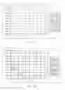
As shown in FIG. 1A to FIG. 1C, FIG. 1A shows a normal capacitance simulation value of a conventional square capacitor whose upper and lower boards have same areas (where that the length is 42 mil, the width is 32 mil, and a vertical distance between the upper and lower boards is 0.02 mm is used as an example). FIG. 1B shows a simulation value (where the length is 41 mil and the width is 31 mil) obtained by adding a negative tolerance to the square capacitor shown in FIG. 1A. FIG. 1C is a simulation value (where the length is 43 mil and the width is 33 mil) obtained by adding a positive tolerance to the square capacitor shown in FIG. 1A.
SUMMARY
In view of this, an objective of the present invention is to provide a circuit substrate, to reduce, by using a structure of an upper circular capacitor board and a lower circular capacitor board, a capacitance value variation caused by a process error.
The circuit substrate includes a first signal end, a second signal end, a first circular capacitor structure, and a second circular capacitor structure. The first circular capacitor structure is electrically connected to the first signal end. The second circular capacitor structure is electrically connected to the second signal end.
The first circular capacitor structure and the second circular capacitor structure are located in different planes of the circuit substrate.
BRIEF DESCRIPTION OF THE DRAWINGS
FIG. 1A to FIG. 1C are curved charts of capacitance value variations of a conventional square capacitor;
FIG. 2A is a three-dimensional diagram of an embodiment of a circuit substrate applicable to an electrical connector according to the present invention;
FIG. 2B is an exploded view of the embodiment in FIG. 2A;
FIG. 3 is a three-dimensional diagram of an embodiment of a circuit substrate according to the present invention;
FIG. 4A is a schematic diagram of an embodiment of a circuit substrate according to the present invention;
FIG. 4B to FIG. 4D are simulation diagrams of the embodiment in FIG. 4A;
FIG. 5A is a simulation diagram of a capacitance value of a conventional square capacitor and that of a circuit substrate of the present invention;
FIG. 5B is a simulation diagram of a conventional square capacitor to which a positive/negative tolerance is added; and
FIG. 5C is a simulation diagram of circuit substrate of the present invention to which a positive/negative tolerance is added.
DETAILED DESCRIPTION
The following describes a plurality of implementations of the present invention with reference to the accompany drawings and words. For clarity, many practical details are described together in the following description. However, it should be understood that, the practical details should not be applied to limit the present invention. In addition, for simplicity, some known structures and elements are drawn in the accompanying drawings in simple and exemplary manners.
Referring to FIG. 2A and FIG. 2B, a circuit substrate 11 in this embodiment is applicable to an electrical connector 1, for example, an electrical connector and a communication connector. This is not specially limited. The electrical connector 1 includes the circuit substrate 11, a mating portion 12, and a circuit board 13. Both the circuit substrate 11 and the circuit board 13 are electrically connected to metal contacts 121 to 128 on the mating portion 12.
Referring to FIG. 3 and FIG. 4A to FIG. 4D. That the circuit substrate 11 in this embodiment is a flexible circuit board is used as an example, but this is not limited thereto. As shown in FIG. 2 to FIG. 3, the circuit substrate 11 preferably includes signal ends 111, 113, 114, 115, 116 and 118, a first circular capacitor structure 11a, and a second circular capacitor structure 11b. The signal ends 111, 113, 114, 115, 116 and 118 are respectively electrically connected to the metal contacts 121 to 128 on the mating portion 12. For example, the first signal end 111 is connected to the metal contact 121, the second signal end 113 is connected to the metal contact 123, and so on.
The first circular capacitor structure 11a is located at an upper layer of the circuit substrate 11, and is electrically connected to the first signal end 111 by using a signal line S1. The second circular capacitor structure 11b is preferably located at a layer different from the layer at which the first circular capacitor structure 11a is located, for example, the second circular capacitor structure 11b is located at a bottom layer, and is electrically connected to the second signal end 113 by using a signal line S3. Based on this design, an electric field may be stored by using the two circular capacitor structures: the upper circular capacitor structure 11a and the lower circular capacitor structure 11b, to further form capacitive coupling.
In this embodiment, that the areas of the first circular capacitor structure 11a and the second circular capacitor structure 11b are the same is used as an example, but this is not limited thereto. However, for ease of recognition, the two circular capacitor structures in the figure are still presented in different sizes.
Referring to FIG. 4B to FIG. 4D, in this embodiment, the radii of both the first circular capacitor structure 11a and the second circular capacitor structure 11b are 20.684 mil (which is learned through conversion of the area of the square capacitor in FIG. 1A), and a vertical distance between the two capacitor boards is also 0.02 mm. When simulation is performed based on this condition, the capacitance values of the circuit substrate are approximately 2.895E−14 F, 2.893E−14 F, 2.892E−14 F, and 2.891E−14 F at different frequencies.
As shown in FIG. 4C and FIG. 4D, FIG. 4C and FIG. 4D are simulation data respectively obtained by adding a negative tolerance and a positive tolerance on the circular capacitor in FIG. 4B (where radii are respectively 20.184 mil and 21.184 mil).
In an embodiment, the circuit substrate may alternatively include a plurality of circular capacitor structures, for example, a third circular capacitor structure 12a and a fourth circular capacitor structure 12b. A third signal end 115 is electrically connected to the third circular capacitor structure 12a by using a signal line S5. The fourth circular capacitor structure 12b is electrically connected to the second signal end 113 by sharing the signal line S3, and the fourth circular capacitor structure 12b is capacitively coupled to the third circular capacitor structure 12a. In this embodiment, that the areas of the two circular capacitor structures are the same is also used as an example.
Based on the foregoing embodiments and referring to FIG. 5A to FIG. 5C, FIG. 5A and FIG. 5B are statistical graphics of simulation capacitance values of a conventional normal square capacitance value and that when a process error occurs. As shown in the figure, by using a conventional square capacitor board as an example (where the areas are the same and a positive tolerance and a negative tolerance are respectively added), capacitance value errors obtained at different frequencies approximately fall between 4.84% and 8.16%.
FIG. 5A also includes a statistical graphic of simulation capacitance values of a normal circular capacitance value and that when a process error occurs according to the present invention. As shown in FIG. 5A and FIG. 5C, by using a circular capacitor board in the present invention as an example (where the areas are the same and a positive tolerance and a negative tolerance are respectively added), capacitance value errors obtained at different frequencies approximately fall between 2.00% and 6.40%.
In conclusion, it can be clearly learned through comparison that the circular capacitor structure of the present invention can effectively reduce a quantity of capacitance value variations caused by positive and negative tolerance of the process. That is, the circular plate capacitor structure has a relatively good efficacy of anti-process error.
The areas of the circuit substrate and the upper and lower boards of the circular capacitor structure of the present invention may be the same or may be different. This is not specifically limited, as described herein.
The circuit substrate of the present invention may also be a hard circuit board, a double-layer board, and a multi-layer board. This is not specifically limited, as described herein.
Compared with the conventional art, the circuit substrate of the present invention reduces, by using a structure of an upper circular capacitor board and a lower circular capacitor board, a capacitance value variation caused by a process error.
LIST OF REFERENCE NUMERALS
| 1 | Electrical connector | 11 | Circuit substrate |
| 12 | Mating portion | 13 | Circuit board |
| 111 | First signal end | 113 | Second signal end |
| 114 | Signal end | 115 | Third signal end |
| 116 | Signal end | 118 | Signal end |
| 121 | Metal contact | 122 | Metal contact |
| 123 | Metal contact | 124 | Metal contact |
| 125 | Metal contact | 126 | Metal contact |
| 127 | Metal contact | 128 | Metal contact |
| 11a | First circular capacitor | 11b | Second circular capacitor |
| structure | structure | ||
| 12a | Third circular capacitor | 12b | Fourth circular capacitor |
| structure | structure | ||
| S1 | Signal line | S3 | Signal line |
| S5 | Signal line | ||
Claims
What is claimed is:1. A circuit substrate, comprising:
a first signal end;
a second signal end;
a first circular capacitor structure, electrically connected to the first signal end; and
a second circular capacitor structure, electrically connected to the second signal end, wherein
the first circular capacitor structure and the second circular capacitor structure are located in different planes of the circuit substrate.
2. The circuit substrate according to claim 1, wherein the areas of the first circular capacitor structure and the second circular capacitor structure are the same.
3. The circuit substrate according to claim 1, wherein the areas of the first circular capacitor structure and the second circular capacitor structure are not the same.
4. The circuit substrate according to claim 1, further comprising:
a third signal end;
a third circular capacitor structure, electrically connected to the third signal end; and
a fourth circular capacitor structure, electrically connected to the second signal end, wherein
the third circular capacitor structure and the fourth circular capacitor structure are located in different planes of the circuit substrate.
5. The circuit substrate according to claim 4, wherein the areas of the third circular capacitor structure and the fourth circular capacitor structure are the same.
Images & Drawings included:


Sources:
- United States Patent and Trademark Office - verify current appl. status at the USPTO↗
Similar patent applications:
- » 11031074
Capacitor material with metal component for use in circuitized substrates, circuitized substrate utilizing same, method of making said circuitized substrate, and information handling system utilizing said circuitized substrate - » 20060151863
Capacitor material for use in circuitized substrates, circuitized substrate utilizing same, method of making said circuitized substrate, and information handling system utilizing said circuitized substrate - » 20060154501
Capacitor material with metal component for use in circuitized substrates, circuitized substrate utilizing same, method of making said circuitized substrate, and information handling system utilizing said circuitized substrate - » 20240332123
SCRIBED CERAMIC CIRCUIT SUBSTRATE, CERAMIC CIRCUIT SUBSTRATE, METHOD FOR PRODUCING SCRIBED CERAMIC CIRCUIT SUBSTRATE, METHOD FOR PRODUCING CERAMIC CIRCUIT SUBSTRATE, AND METHOD FOR PRODUCING SEMICONDUCTOR DEVICE - » 10668777
Manufacturing method of circuit substrate, circuit substrate and manufacturing device of circuit substrate - » 20160118436
Method of manufacturing an image sensor by joining a pixel circuit substrate and a logic circuit substrate and thereafter thinning the pixel circuit substrate - » 20150004738
Method of manufacturing an image sensor by joining a pixel circuit substrate and a logic circuit substrate and thereafter thinning the pixel circuit substrate - » 20070010065
Method of making a capacitive substrate for use as part of a larger circuitized substrate, method of making said circuitized substrate and method of making an information handling system including said circuitized substrate - » 20070010064
Method of making a capacitive substrate using photoimageable dielectric for use as part of a larger circuitized substrate, method of making said circuitized substrate and method of making an information handling system including said circuitized substrate - » 20060023935
Printed circuit substrate appearance inspection method, printed circuit substrate appearance inspection program and printed circuit substrate appearance inspection apparatus
Recent applications in this class:
- » 20250007219 2025-01-02
COMMUNICATION CONNECTOR APPARATUS - » 20240204460 2024-06-20
TELECOMMUNICATIONS DEVICE - » 20240195125 2024-06-13
Multistage capacitive crosstalk compensation arrangement - » 20230402793 2023-12-14
Electronic device with cable interface and manufacturing method thereof - » 20230307875 2023-09-28
Telecommunications device - » 20220224051 2022-07-14
Telecommunications device - » 20220013961 2022-01-13
MULTISTAGE CAPACITIVE CROSSTALK COMPENSATION ARRANGEMENT - » 20210328382 2021-10-21
Methods and systems for compensating for alien crosstalk between connectors - » 20210281017 2021-09-09
MULTICORE CABLE-WITH-CONNECTOR - » 20210194181 2021-06-24
Telecommunications device
Recent applications for this Assignee:
- » 20220183462 2022-06-16
Package tray and case module including the package tray - » 20220140517 2022-05-05
Electrical connector with adjustable wire inlet hole - » 20220131315 2022-04-28
Electrical plug - » 20210184390 2021-06-17
Connector mounting rack and patch panel system thereof - » 20210135413 2021-05-06
Signal communication socket - » 20190353526 2019-11-21
Sensor and automatic calibration method applied thereto - » 20190074651 2019-03-07
Electrical connector - » 20160344363 2016-11-24
Circuit board - » 20150011119 2015-01-08
Rotatable frame, connector, and connector support system - » 20140179137 2014-06-26
Data cabling jack device and data cabling assembly structure