Carrier warpage control for three dimensional integrated circuit (3DIC) stacking
US20190267255A1
2019-08-29
16/410,842
2019-05-13
✅ Patent granted
US 10,825,693 B2
2020-11-03
-
-
Savitri Mulpuri
Slater Matsil, LLP
2039-05-13
Abstract:
An embodiment method of forming a package-on-package (PoP) device includes temporarily mounting a substrate on a carrier, stacking a first die on the substrate, at least one of the die and the substrate having a coefficient of thermal expansion mismatch relative to the carrier, and stacking a second die on the first die. The substrate may be formed from one of an organic substrate, a ceramic substrate, a silicon substrate, a glass substrate, and a laminate substrate.
Inventors:
- Jing-Cheng LIN 218 🇹🇼 Hsinchu, Taiwan
- Chen-Hua YU 1,372 🇹🇼 Hsinchu, Taiwan
- Shih Ting Lin 47 🇹🇼 Taipei, Taiwan
Assignee:
- Taiwan Semiconductor Manufacturing Company 371 🇹🇼 Hsin-Chu, Taiwan
Applicant:
Interested in similar patents?
Get notified when new applications in this technology area are published.
Classification:
H01L23/31 IPC
Details of semiconductor or other solid state devices; Encapsulations, e.g. encapsulating layers, coatings, e.g. for protection characterised by the arrangement or shape
H01L21/561 » CPC further
Processes or apparatus adapted for the manufacture or treatment of semiconductor or solid state devices or of parts thereof; Manufacture or treatment of semiconductor devices or of parts thereof the devices having at least one potential-jump barrier or surface barrier, e.g. PN junction, depletion layer or carrier concentration layer; Assembly of semiconductor devices using processes or apparatus not provided for in a single one of the subgroups - , e.g. sealing of a cap to a base of a container; Encapsulations, e.g. encapsulation layers, coatings Batch processing
H01L21/563 » CPC further
Processes or apparatus adapted for the manufacture or treatment of semiconductor or solid state devices or of parts thereof; Manufacture or treatment of semiconductor devices or of parts thereof the devices having at least one potential-jump barrier or surface barrier, e.g. PN junction, depletion layer or carrier concentration layer; Assembly of semiconductor devices using processes or apparatus not provided for in a single one of the subgroups - , e.g. sealing of a cap to a base of a container; Encapsulations, e.g. encapsulation layers, coatings Encapsulation of active face of flip-chip device, e.g. underfilling or underencapsulation of flip-chip, encapsulation preform on chip or mounting substrate
H01L21/568 » CPC further
Processes or apparatus adapted for the manufacture or treatment of semiconductor or solid state devices or of parts thereof; Manufacture or treatment of semiconductor devices or of parts thereof the devices having at least one potential-jump barrier or surface barrier, e.g. PN junction, depletion layer or carrier concentration layer; Assembly of semiconductor devices using processes or apparatus not provided for in a single one of the subgroups - , e.g. sealing of a cap to a base of a container; Encapsulations, e.g. encapsulation layers, coatings Temporary substrate used as encapsulation process aid
H01L23/3128 » CPC further
Details of semiconductor or other solid state devices; Encapsulations, e.g. encapsulating layers, coatings, e.g. for protection characterised by the arrangement or shape the device being completely enclosed a substrate forming part of the encapsulation the substrate having spherical bumps for external connection
H01L24/96 » CPC further
Arrangements for connecting or disconnecting semiconductor or solid-state bodies; Methods or apparatus related thereto; Batch processes at chip-level, i.e. with connecting carried out on a plurality of singulated devices, i.e. on diced chips the devices being encapsulated in a common layer, e.g. neo-wafer or pseudo-wafer, said common layer being separable into individual assemblies after connecting
H01L24/97 » CPC further
Arrangements for connecting or disconnecting semiconductor or solid-state bodies; Methods or apparatus related thereto; Batch processes at chip-level, i.e. with connecting carried out on a plurality of singulated devices, i.e. on diced chips the devices being connected to a common substrate, e.g. interposer, said common substrate being separable into individual assemblies after connecting
H01L25/0657 » CPC further
Assemblies consisting of a plurality of individual semiconductor or other solid state devices ; Multistep manufacturing processes thereof all the devices being of a type provided for in the same subgroup of groups - , e.g. assemblies of rectifier diodes the devices not having separate containers the devices being of a type provided for in group Stacked arrangements of devices
H01L24/13 » CPC further
Arrangements for connecting or disconnecting semiconductor or solid-state bodies; Methods or apparatus related thereto; Means for bonding being attached to, or being formed on, the surface to be connected, e.g. chip-to-package, die-attach, "first-level" interconnects; Manufacturing methods related thereto; Bump connectors ; Manufacturing methods related thereto; Structure, shape, material or disposition of the bump connectors prior to the connecting process of an individual bump connector
H01L24/16 » CPC further
Arrangements for connecting or disconnecting semiconductor or solid-state bodies; Methods or apparatus related thereto; Means for bonding being attached to, or being formed on, the surface to be connected, e.g. chip-to-package, die-attach, "first-level" interconnects; Manufacturing methods related thereto; Bump connectors ; Manufacturing methods related thereto; Structure, shape, material or disposition of the bump connectors after the connecting process of an individual bump connector
H01L24/32 » CPC further
Arrangements for connecting or disconnecting semiconductor or solid-state bodies; Methods or apparatus related thereto; Means for bonding being attached to, or being formed on, the surface to be connected, e.g. chip-to-package, die-attach, "first-level" interconnects; Manufacturing methods related thereto; Layer connectors, e.g. plate connectors, solder or adhesive layers; Manufacturing methods related thereto; Structure, shape, material or disposition of the layer connectors after the connecting process of an individual layer connector
H01L24/73 » CPC further
Arrangements for connecting or disconnecting semiconductor or solid-state bodies; Methods or apparatus related thereto Means for bonding being of different types provided for in two or more of groups , , , , , , ,
H01L24/81 » CPC further
Arrangements for connecting or disconnecting semiconductor or solid-state bodies; Methods or apparatus related thereto; Methods for connecting semiconductor or other solid state bodies using means for bonding being attached to, or being formed on, the surface to be connected using a bump connector
H01L24/92 » CPC further
Arrangements for connecting or disconnecting semiconductor or solid-state bodies; Methods or apparatus related thereto; Methods for connecting semiconductor or solid state bodies including different methods provided for in two or more of groups - Specific sequence of method steps
H01L2224/73204 » CPC further
Indexing scheme for arrangements for connecting or disconnecting semiconductor or solid-state bodies and methods related thereto as covered by; Means for bonding being of different types provided for in two or more of groups; Location after the connecting process on the same surface; Bump and layer connectors the bump connector being embedded into the layer connector
H01L2224/81005 » CPC further
Indexing scheme for arrangements for connecting or disconnecting semiconductor or solid-state bodies and methods related thereto as covered by; Methods for connecting semiconductor or other solid state bodies using means for bonding being attached to, or being formed on, the surface to be connected using a bump connector involving a temporary auxiliary member not forming part of the bonding apparatus being a temporary or sacrificial substrate
H01L2224/83005 » CPC further
Indexing scheme for arrangements for connecting or disconnecting semiconductor or solid-state bodies and methods related thereto as covered by; Methods for connecting semiconductor or other solid state bodies using means for bonding being attached to, or being formed on, the surface to be connected using a layer connector involving a temporary auxiliary member not forming part of the bonding apparatus being a temporary or sacrificial substrate
H01L2224/92125 » CPC further
Indexing scheme for arrangements for connecting or disconnecting semiconductor or solid-state bodies and methods related thereto as covered by; Methods for connecting semiconductor or solid state bodies including different methods provided for in two or more of groups - ; Specific sequence of method steps; Connecting a surface with connectors of different types; Sequential connecting processes the first connecting process involving a bump connector the second connecting process involving a layer connector
H01L2224/97 » CPC further
Indexing scheme for arrangements for connecting or disconnecting semiconductor or solid-state bodies and methods related thereto as covered by; Batch processes at chip-level, i.e. with connecting carried out on a plurality of singulated devices, i.e. on diced chips the devices being connected to a common substrate, e.g. interposer, said common substrate being separable into individual assemblies after connecting
H01L2225/06517 » CPC further
Details relating to assemblies covered by the group but not provided for in its subgroups; All the devices being of a type provided for in the same subgroup of groups - the devices not having separate containers the devices being of a type provided for in group; Stacked arrangements of devices Bump or bump-like direct electrical connections from device to substrate
H01L2225/06541 » CPC further
Details relating to assemblies covered by the group but not provided for in its subgroups; All the devices being of a type provided for in the same subgroup of groups - the devices not having separate containers the devices being of a type provided for in group; Stacked arrangements of devices Conductive via connections through the device, e.g. vertical interconnects, through silicon via [TSV]
H01L2225/06562 » CPC further
Details relating to assemblies covered by the group but not provided for in its subgroups; All the devices being of a type provided for in the same subgroup of groups - the devices not having separate containers the devices being of a type provided for in group; Stacked arrangements of devices; Geometry of the stack, e.g. form of the devices, geometry to facilitate stacking at least one device in the stack being rotated or offset
H01L2225/06565 » CPC further
Details relating to assemblies covered by the group but not provided for in its subgroups; All the devices being of a type provided for in the same subgroup of groups - the devices not having separate containers the devices being of a type provided for in group; Stacked arrangements of devices; Geometry of the stack, e.g. form of the devices, geometry to facilitate stacking the devices having the same size and there being no auxiliary carrier between the devices
H01L2924/141 » CPC further
Indexing scheme for arrangements or methods for connecting or disconnecting semiconductor or solid-state bodies as covered by; Details of semiconductor or other solid state devices to be connected; Device type; Integrated circuits Analog devices
H01L2924/1431 » CPC further
Indexing scheme for arrangements or methods for connecting or disconnecting semiconductor or solid-state bodies as covered by; Details of semiconductor or other solid state devices to be connected; Device type; Integrated circuits; Digital devices Logic devices
H01L2924/1434 » CPC further
Indexing scheme for arrangements or methods for connecting or disconnecting semiconductor or solid-state bodies as covered by; Details of semiconductor or other solid state devices to be connected; Device type; Integrated circuits; Digital devices Memory
H01L2924/157 » CPC further
Indexing scheme for arrangements or methods for connecting or disconnecting semiconductor or solid-state bodies as covered by; Details of package parts other than the semiconductor or other solid state devices to be connected; Die mounting substrate; Material with a principal constituent of the material being a metal or a metalloid, e.g. boron [B], silicon [Si], germanium [Ge], arsenic [As], antimony [Sb], tellurium [Te] and polonium [Po], and alloys thereof
H01L2924/15311 » CPC further
Indexing scheme for arrangements or methods for connecting or disconnecting semiconductor or solid-state bodies as covered by; Details of package parts other than the semiconductor or other solid state devices to be connected; Die mounting substrate; Connection portion the connection portion being formed only on the surface of the substrate opposite to the die mounting surface being a ball array, e.g. BGA
H01L2924/15788 » CPC further
Indexing scheme for arrangements or methods for connecting or disconnecting semiconductor or solid-state bodies as covered by; Details of package parts other than the semiconductor or other solid state devices to be connected; Die mounting substrate; Material with a principal constituent of the material being a non metallic, non metalloid inorganic material Glasses, e.g. amorphous oxides, nitrides or fluorides
H01L2924/18161 » CPC further
Indexing scheme for arrangements or methods for connecting or disconnecting semiconductor or solid-state bodies as covered by; Details of package parts other than the semiconductor or other solid state devices to be connected; Encapsulation; Shape; Exposing the passive side of the semiconductor or solid-state body of a flip chip
H01L25/065 IPC
Assemblies consisting of a plurality of individual semiconductor or other solid state devices ; Multistep manufacturing processes thereof all the devices being of a type provided for in the same subgroup of groups - , e.g. assemblies of rectifier diodes the devices not having separate containers the devices being of a type provided for in group
H01L21/56 » CPC main
Processes or apparatus adapted for the manufacture or treatment of semiconductor or solid state devices or of parts thereof; Manufacture or treatment of semiconductor devices or of parts thereof the devices having at least one potential-jump barrier or surface barrier, e.g. PN junction, depletion layer or carrier concentration layer; Assembly of semiconductor devices using processes or apparatus not provided for in a single one of the subgroups - , e.g. sealing of a cap to a base of a container Encapsulations, e.g. encapsulation layers, coatings
H01L24/83 » CPC further
Arrangements for connecting or disconnecting semiconductor or solid-state bodies; Methods or apparatus related thereto; Methods for connecting semiconductor or other solid state bodies using means for bonding being attached to, or being formed on, the surface to be connected using a layer connector
H01L2225/06513 » CPC further
Details relating to assemblies covered by the group but not provided for in its subgroups; All the devices being of a type provided for in the same subgroup of groups - the devices not having separate containers the devices being of a type provided for in group; Stacked arrangements of devices Bump or bump-like direct electrical connections between devices, e.g. flip-chip connection, solder bumps
H01L2924/15787 » CPC further
Indexing scheme for arrangements or methods for connecting or disconnecting semiconductor or solid-state bodies as covered by; Details of package parts other than the semiconductor or other solid state devices to be connected; Die mounting substrate; Material with a principal constituent of the material being a non metallic, non metalloid inorganic material Ceramics, e.g. crystalline carbides, nitrides or oxides
H01L2924/351 » CPC further
Indexing scheme for arrangements or methods for connecting or disconnecting semiconductor or solid-state bodies as covered by; Technical effects; Mechanical effects Thermal stress
H01L2924/3511 » CPC further
Indexing scheme for arrangements or methods for connecting or disconnecting semiconductor or solid-state bodies as covered by; Technical effects; Mechanical effects; Thermal stress Warping
H01L23/00 IPC
Details of semiconductor or other solid state devices
Description
CROSS-REFERENCE TO RELATED APPLICATIONS
This application is a continuation of U.S. patent application Ser. No. 16/050,954, filed on Jul. 31, 2018, which is a divisional of U.S. patent application Ser. No. 13/779,554, filed on Feb. 27, 2013 and entitled “Carrier Warpage Control for Three Dimensional Integrated Circuit (3DIC) Stacking,” now U.S. patent Ser. No. 10/153,179, issued Dec. 11, 2018, which claims the benefit of U.S. Provisional Application No. 61/693,083, filed on Aug. 24, 2012, entitled “Carrier Warpage Control for 3DIC Stacking,” which applications are hereby incorporated herein by reference.
BACKGROUND
As the demand for smaller electronic products grows, manufacturers and others in the electronics industry continually seek ways to reduce the size of integrated circuits used in the electronic products. In that regard, three-dimensional type integrated circuit packaging techniques have been developed and used.
One packaging technique that has been developed is Package-on-Package (PoP). As the name implies, PoP is a semiconductor packaging innovation that involves stacking one package on top of another package. A PoP device may combine vertically discrete memory and logic packages.
Unfortunately, conventional processes used to fabricate the PoP devices may not be able to sufficiently prevent the packages from warping. This is particularly true when relatively thin dies or integrated circuits are being stacked.
BRIEF DESCRIPTION OF THE DRAWINGS
For a more complete understanding of the present disclosure, and the advantages thereof, reference is now made to the following descriptions taken in conjunction with the accompanying drawings, in which:
FIGS. 1A-1I collectively illustrate an embodiment method of forming a PoP device using a carrier to inhibit or prevent warping in stacked dies;
FIG. 2 illustrates a cross sectional view of an embodiment PoP device formed using the method of FIGS. 1A-1I;
FIG. 3 illustrates a cross sectional view of an embodiment PoP device formed using the method of FIGS. 1A-1I without any underfill; and
FIG. 4 illustrates a cross sectional view of an embodiment PoP device formed using the method of FIGS. 1A-1I without any molding on sidewalls of the substrate.
Corresponding numerals and symbols in the different figures generally refer to corresponding parts unless otherwise indicated. The figures are drawn to clearly illustrate the relevant aspects of the embodiments and are not necessarily drawn to scale.
DETAILED DESCRIPTION OF ILLUSTRATIVE EMBODIMENTS
The making and using of the presently present embodiments are discussed in detail below. It should be appreciated, however, that the present disclosure provides many applicable inventive concepts that can be embodied in a wide variety of specific contexts. The specific embodiments discussed are merely illustrative and do not limit the scope of the disclosure.
The present disclosure will be described with respect to present embodiments in a specific context, namely a package-on-package (PoP) semiconductor device. The concepts in the disclosure may also apply, however, to other semiconductor structures or circuits.
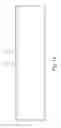
Referring now to FIGS. 1A-1I, an embodiment method of forming a PoP device 10 (FIGS. 2-4) is collectively illustrated. As shown in FIG. 1A, glue 12 or another suitable bonding material is deposited or formed on a carrier 14. In an embodiment, the carrier 14 is formed from glass, silicon, a material having a low coefficient of thermal expansion, or another suitable carrier material. Indeed, the carrier 14 is generally a higher modulus material with good stiffness.
Referring now to FIG. 1B, a substrate 16 is temporarily mounted on the carrier 14 using the glue 12 or other suitable bonding material. In an embodiment, the substrate 16 is an organic substrate, a ceramic substrate, a silicon substrate, a glass substrate, or a laminate substrate having or supporting metal interconnects 18 or metallization. In an embodiment, the substrate 16 is formed from an epoxy, a resin, or another material.
Referring now to FIG. 1C, in an embodiment a pressure anneal is performed after the substrate 16 has been temporarily mounted on the carrier 14 as shown in FIG. 1B. The pressure anneal generally biases the substrate 16 toward the carrier 14. This ensures that the substrate 16 is securely mounted, albeit temporarily, on the carrier 14. In an embodiment, the pressure anneal of FIG. 1C is performed using a pressure anneal cap 20 along with heating. In an embodiment, pressure anneal may be performed later in the embodiment method illustrated in FIGS. 1A-1I. For example, the pressure anneal may be performed on a wafer, on a panel, on a single unit, or on multiple units. In addition, in an embodiment the pressure anneal includes pressure only without the application of heat.
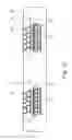
Referring now to FIG. 1D, after the pressure anneal cap 20 of FIG. 1C has been removed, a first die 22 is attached to the substrate 16 using, for example, solder balls and corresponding contact pads. The first die 22 may include logic components (a logic integrated circuit, analog circuit, etc.), a memory component, and so on. The substrate 16 and/or the die 22 generally have a material coefficient of thermal expansion mismatch relative to the carrier 14. As will be more fully explained below, any warping of, for example, dies or other semiconductor structures stacked on or over the substrate 16 is inhibited or prevented.
After placing the first die 22, an underfill material 24 may be flowed between the first die 22 and the substrate 16. In an embodiment, the underfill material 24 is omitted between the first die 22 and the substrate 16.
Referring now to FIG. 1E, after the first die 22 has been mounted, a second die 26 is attached over the first die 22 using, for example, solder balls and corresponding contact pads. The second die 26 may include logic components (a logic integrated circuit, analog circuit, etc.), a memory component, and so on. Notably, the stacking of the second die 26 upon the first die 22 generally forms the PoP devices 10.
After placing the second die 26 as shown in FIG. 1E, an underfill material 24 may be flowed between the second die 26 and the first die 22. In an embodiment, the underfill material 24 is omitted. As will be more fully explained below, in an embodiment the second die 26 may be horizontally offset relative to the first die 22 to provide the second die 26 with an overhang.
Referring now to FIG. 1F, after the second die 26 has been mounted, a molding material 28 is formed over, for example, exposed portions of the substrate 16, the first die 22, and the second die 26. In an embodiment, the molding material 28 is also formed over the glue 12 disposed on the carrier 14 and adjacent to the substrate 16. In an embodiment, the molding material 28 generally encapsulates the first and second dies 22, 26.
Referring now to FIG. 1G, after the molding material 28 has been formed over the first and second dies 22, 26, a grinding process is performed to remove an upper portion of the molding material 28. As shown, the grinding process may expose a top surface of the second die 26. However, in an embodiment, the grinding process may leave a portion or thin layer of the molding material 28 disposed over the second die 26.
Referring now to FIG. 1H, after the grinding process has been performed, the assembly is flipped over and a de-bonding process is performed to remove the carrier 14 from the substrate 16. In addition, a cleaning process is performed to remove the glue 12 from the substrate 16 and the molding material 28. Once the de-bonding and cleaning processes have been performed, contact pads from the metal interconnects 18 of the substrate 16 are exposed.
Referring now to FIG. 1I, after the de-bonding and cleaning processes have been performed, a ball mount process is performed to form an array of solder balls 30 on the contact pads from the metal interconnects 18 of the substrate 16. In addition, a wafer saw process is performed to separate the PoP devices 10 from each other. As shown in FIG. 1I, after the wafer saw process a portion of the molding material 28 still covers the sidewalls 32 of the substrate 16. However, in an embodiment the wafer saw process removes the molding material 28 from the sidewalls 32 of the substrate 16.
Referring to FIG. 2, an embodiment PoP device 10 formed using an embodiment method is illustrated. As shown, the PoP device 10 includes a first die 22 stacked on the substrate 16 and a second die 26 stacked on the first die 22. In an embodiment, the second die 26 is horizontally offset relative to the first die 22 to provide the second die 26 with the overhang 34 noted above.
In an embodiment, the underfill material 24 is disposed between the substrate 16 and the first die 22 as well as between the first die 22 and the second die 26. In an embodiment, the underfill material 24 is disposed between the substrate 16 and the first die 22 only. In an embodiment, the underfill material 24 is disposed between the first die 22 and the second die 26 only. In addition, the molding material 28 of the PoP device 10 has been formed around portions of the substrate 16, the first die 22, and the second die 26. In an embodiment, the molding material 28 is omitted.
Still referring to FIG. 2, the substrate 16 of the PoP device 10 supports metal interconnects 18 and/or other connection structures (e.g., under bump metallization) used to electrically couple the solder balls 30 (i.e., the ball grid array) to the first die 22. The PoP device 10 may also include other structures, layers, or materials such as, for example, passivation layers, through silicon vias (TSVs), aluminum pads, solder, and so on.
Referring now to FIG. 3, in an embodiment the underfill material 24 of FIG. 2 has been omitted from the PoP device 10 and replaced by the molding material 28. In other words, the molding material 28 functions or preforms as an underfill in the embodiment PoP device 10 of FIG. 3.
Referring now to FIG. 4, in an embodiment the molding material 28 is left off or removed from sidewalls 32 of the substrate 16. By way of example, the molding material 28 may not be formed on the sidewalls 32 when the molding material 28 is deposited during the molding process of FIG. 1F. In other words, the molding material 28 is prevented from forming on the sidewalls 32. In another example, the molding material 28 may be removed from the sidewalls 32 of the substrate 16 using the wafer saw process of FIG. 1I. In other words, the wafer saw removes the molding material 28 from the sidewalls 32.
It should be recognized that the embodiment methods and PoP device 10 provide numerous advantages. Indeed, by using the carrier 14 during the stacking of dies 22, 26 warping is inhibited or prevented, even when relatively thin dies are stacked. In addition, multiple dies may be stacked, either with or without an overhang.
An embodiment method of forming a package-on-package (PoP) device includes temporarily mounting a substrate on a carrier, stacking a first die on the substrate, at least one of the die and the substrate having a coefficient of thermal expansion mismatch relative to the carrier, and stacking a second die on the first die.
An embodiment method of forming a package-on-package (PoP) device includes temporarily mounting a substrate on a carrier, stacking a plurality of dies over the substrate, at least one of the plurality of dies and the substrate having a coefficient of thermal expansion mismatch relative to the carrier, and removing the carrier after the plurality of dies have been stacked.
A embodiment method of forming a package-on-package (PoP) device includes temporarily mounting a substrate on a carrier, stacking a first die on the substrate, at least one of the first die and the substrate having a coefficient of thermal expansion mismatch relative to the carrier, stacking a second die on the first die, the second die horizontally offset relative to the first die to provide the second die with an overhang, and flowing an underfill material between the first die and the substrate and between the first die and the second die.
While this disclosure has been described with reference to illustrative embodiments, this description is not intended to be construed in a limiting sense. Various modifications and combinations of the illustrative embodiments, as well as other embodiments of the disclosure, will be apparent to persons skilled in the art upon reference to the description. It is therefore intended that the appended claims encompass any such modifications or embodiments.
Claims
What is claimed is:1. A package-on-package (PoP) device comprising:
a first die over and electrically connected to a first substrate, wherein the first die comprises:
a second substrate;
a through via extending through the second substrate;
a first passivation layer on a first side of the second substrate;
a second passivation layer on a second side of the second substrate;
a first conductive pillar on the first side of the first substrate and electrically connected to the through via; and
a second conductive pillar on the second side of the first substrate and electrically connected to the through via; and
a second die over the first die and electrically connected to the first die, wherein the second die is horizontally offset relative to the first die.
2. The PoP device of claim 1, further comprising:
a first solder region between the first conductive pillar and the first substrate; and
a second solder region between the second conductive pillar and the second die.
3. The PoP device of claim 1, further comprising:
a first aluminum pad between the first conductive pillar and the through via; and
a second aluminum pad between the second conductive pillar and the through via.
4. The PoP device of claim 3, wherein the first conductive pillar extends through the first passivation layer to the first aluminum pad, and wherein the second conductive pillar extends through the second passivation layer to the second aluminum pad.
5. The PoP device of claim 1, wherein a sidewall of the first conductive pillar is spaced part from a sidewall of the first passivation layer, and wherein a sidewall of the second conductive pillar is spaced part from a sidewall of the second passivation layer.
6. The PoP device of claim 1 further comprising a first underfill between the first die and the second die.
7. The PoP device of claim 6, wherein a portion of a bottom surface of the second die is free of the first underfill.
8. The PoP device of claim 6 further comprising a molding material over the first substrate, around the first die, and around the second die, wherein the molding material physically contacts a bottom surface of the second die.
9. The PoP device of claim 8, wherein an interface between the first underfill and the molding material intersects the bottom surface of the second die.
10. The PoP device of claim 8, wherein sidewalls of the first substrate are free of the molding material.
11. The PoP device of claim 1, wherein the first substrate is an organic substrate, a ceramic substrate, a silicon substrate, a glass substrate, or a laminate substrate having conductive features disposed therein.
12. The PoP device of claim 1, wherein the first conductive pillar comprises three different conductive materials.
13. A package-on-package (PoP) device comprising
a substrate having a conductive feature;
a first die attached to the substrate, wherein the first die has a thickness measured along a first direction between an uppermost surface of the first die and a lowermost surface of the first die, wherein the first die has a through via, wherein a length of the through via, measured along the first direction, is smaller than the thickness of the first die, wherein the through via of the first die is electrically coupled to the conductive feature of the substrate;
a first underfill material between the first die and the substrate;
a second die attached to the first die, the first die being between the second die and the substrate, a first portion of the second die disposed within lateral extents of the first die, a second portion of the second die disposed outside the lateral extents of the first die, wherein a connector of the second die is electrically coupled to the through via of the first die;
a second underfill material between the first die and the second die; and
a molding material over the substrate and contacting the substrate, the molding material surrounding the first die, the second die, the first underfill material, and the second underfill material.
14. The PoP device of claim 13, wherein the through via of the first die is disposed between the uppermost surface of the first die and the lowermost surface of the first die without contacting the uppermost surface and without contacting the lowermost surface.
15. The PoP device of claim 13, wherein the first die further comprises:
a first aluminum pad on the uppermost surface of the first die; and
a second aluminum pad on the lowermost surface of the first die, wherein the through via of the first die is disposed between, and contacts, the first aluminum pad and the second aluminum pad.
16. The PoP device of claim 13, further comprising:
a first solder region between the substrate and the first die; and
a second solder region between the first die and the second die.
17. The PoP device of claim 16, wherein sidewalls of the substrate is free of the molding material.
18. A package-on-package (PoP) device comprising:
a substrate having conductive lines and vias;
a second die on a first side of the substrate, the second die electrically coupled to the substrate;
a first die between the substrate and the second die, wherein the first die is electrically coupled between the substrate and the second die, wherein a first portion of the second die extends within lateral extents of the first die defined by sidewalls of the first die, and a second portion of the second die extends beyond the lateral extents of the first die, wherein the first die comprises:
a first substrate with an upper surface and a lower surface;
a first aluminum pad extending along the upper surface of the first substrate and a second aluminum pad extending along the lower surface of the first substrate;
passivation layers on the upper surface and on the lower surface of the first substrate, wherein the passivation layers cover a portion of the first aluminum pad and a portion of the second aluminum pad;
a through via in the first substrate, wherein the through via is between the first aluminum pad and the second aluminum pad, wherein the through via is electrically coupled to the substrate and the second die; and
a molding material on the substrate and contacting the substrate, wherein the molding material surrounds the first die and the second die.
19. The PoP device of claim 18, wherein the first die further comprises:
a first connector at the upper surface of the first die, the first connector electrically coupled to the first aluminum pad, wherein the first connector is electrically coupled to a connector of the second die; and
a second connector at the lower surface of the first die, the second connector electrically coupled to the second aluminum pad, wherein the second connector is electrically coupled to a conductive line of the substrate.
20. The PoP device of claim 18, further comprising solder balls on a second side of the substrate opposing the first side of the substrate.
Images & Drawings included:


Sources:
- United States Patent and Trademark Office - verify current appl. status at the USPTO↗
Similar patent applications:
Recent applications in this class:
- » 20250293050 2025-09-18
WAFER PROCESSING METHOD AND WAFER PROCESSING APPARATUS - » 20250273481 2025-08-28
METHOD OF MANUFACTURING SEMICONDUCTOR DEVICES AND CORRESPONDING DEVICE - » 20250210375 2025-06-26
SURFACE TREATMENT COMPOSITION AND METHOD FOR PRODUCING WAFER - » 20250191939 2025-06-12
SEMICONDUCTOR DEVICES AND METHODS OF MANUFACTURING - » 20250191938 2025-06-12
Overmolding Structures in Glass - » 20250149346 2025-05-08
METHOD OF FORMING ELECTROMAGNETIC-WAVE SHIELD, METHOD OF MANUFACTURING STRUCTURE, AND STRUCTURE - » 20250096008 2025-03-20
PACKAGED SEMICONDUCTOR DEVICES AND METHODS OF PACKAGING SEMICONDUCTOR DEVICES - » 20250062137 2025-02-20
POWER SEMICONDUCTOR MODULE ARRANGEMENT AND METHOD FOR PRODUCING THE SAME - » 20250062136 2025-02-20
Packages with Implantation - » 20250014912 2025-01-09
METHOD FOR PROTECTING ACTIVE LAYERS OF ELECTRONIC CHIPS
Recent applications for this Assignee:
- » 20230395588 2023-12-07
Semiconductor device packages, packaging methods, and packaged semiconductor devices - » 20230343634 2023-10-26
Mechanism for finFET well doping - » 20230207531 2023-06-29
Semiconductor package for thermal dissipation - » 20230112658 2023-04-13
Methods for non-resist nanolithography - » 20230107176 2023-04-06
Interconnect structure having a carbon-containing barrier layer - » 20220320029 2022-10-06
Dummy structure of stacked and bonded semiconductor device - » 20220302079 2022-09-22
Tools and systems for processing semiconductor devices, and methods of processing semiconductor devices - » 20220288627 2022-09-15
Spin dispenser module substrate surface protection system - » 20220189942 2022-06-16
Semiconductor device packages, packaging methods, and packaged semiconductor devices - » 20210358799 2021-11-18
Mechanism for FinFET well doping