Magnetic-free non-reciprocal circuits based on sub-harmonic spatio-temporal conductance modulation
US20190305397A1
2019-10-03
16/318,074
2017-07-21
✅ Patent granted
US 11,031,665 B2
2021-06-08
WO; PCT/US2017/043402; 20170721
WO; WO2018/075113; 20180426
Dinh T Le
Byrne Poh LLP
2037-07-21
Abstract:
A circuit comprising a differential transmission line and eight switches provides non-reciprocal signal flow. In some embodiments, the circuit can be driven by four local oscillator signals. The circuit can be used to form a gyrator. The circuit can be used to form a circulator. The circuit can be used to form three-port circulator than can provide direction signal flow between a transmitter and an antenna and from the antenna to a receiver. The three-port circulator can be used to implement a full duplex transceiver that uses a single antenna for transmitting and receiving.
Inventors:
- Harish Krishnaswamy 37 🇺🇸 New York, NY, United States
- Tolga Dinc 4 🇺🇸 New York, NY, United States
Assignee:
- The Trustees of Columbia University in the City of New York 2,382 🇺🇸 New York, NY, United States
- The Trustees of Columbia in the City of New York 8 🇺🇸 New York, NY, United States
Applicant:
Interested in similar patents?
Get notified when new applications in this technology area are published.
Classification:
H03D7/16 IPC
Transference of modulation from one carrier to another, e.g. frequency-changing Multiple-frequency-changing
H03D7/165 » CPC further
Transference of modulation from one carrier to another, e.g. frequency-changing; Multiple-frequency-changing at least two frequency changers being located in different paths, e.g. in two paths with carriers in quadrature
H01P1/38 » CPC main
Auxiliary devices; Non-reciprocal transmission devices Circulators
H04L5/14 » CPC further
Arrangements affording multiple use of the transmission path Two-way operation using the same type of signal, i.e. duplex
H03D2200/0003 » CPC further
Indexing scheme relating to details of demodulation or transference of modulation from one carrier to another covered by; Circuit elements of demodulators Rat race couplers
H01P1/383 » CPC further
Auxiliary devices; Non-reciprocal transmission devices; Circulators Junction circulators, e.g. Y-circulators
Description
BACKGROUND
Full-duplex communications, in which a transmitter and a receiver of a transceiver operate simultaneously on the same frequency band, is drawing significant interest for emerging 5G communication networks due to its potential to double network capacity compared to half-duplex communications. Additionally, there are several efforts underway to include simultaneous transmit and receive functionality in the next generation phased array radar systems, especially in commercial automotive radars which can be an enabler technology for future connected or driverless cars. However, one of the biggest challenges from an implementation perspective is the antenna interface.
One way in which an antenna interface for a full-duplex transceiver can be implemented is using a non-reciprocal circulator. Reciprocity in electronics is a fundamental property of linear systems and materials described by symmetric and time-independent permittivity and permeability tensors. Non-reciprocity causes signals to travel in only one direction. For example, non-reciprocity in a circulator causes signals to travel in only one direction through the circulator. This directional signal flow enables full-duplex wireless communications because signals from the transmitter are only directed toward the antenna (and not the receiver) and received signals at the antenna are only directed toward the receiver (and not the transmitter). Moreover, the receiver is isolated from signals from the transmitter, preventing desensitization and possible breakdown of the receiver due to the high-power transmitted signal.
Conventionally, non-reciprocal circulators have been implemented using ferrite materials, which are materials that lose their reciprocity under the application of an external magnetic field. However, ferrite materials cannot be integrated into CMOS IC technology. Furthermore, the need for an external magnet renders ferrite-based circulators bulky and expensive.
Accordingly, new mechanisms for implementing non-reciprocity in circuits is desirable.
DETAILED DESCRIPTION
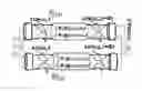
FIGS. 1A, 1B, 1C, and 1D show an example of how a non-reciprocal phase shift can be implemented in some embodiments.
Turning to FIG. 1A, it can be seen that a signal cos(ωint) can be injected at nodes A. This is represented in graph 101 of FIG. 1B. As shown in FIG. 1A, the switch groups can then be switched by the following signals: cos(ωmt); cos(ωmt+ϕ); sin(ωmt); and sin(ωint+ϕ), where ϕ is 90°. ϕ1 and ϕ2 shown in FIGS. 1A and 1B relate to ϕ according to the following equation: 2ϕ=180=ϕ1−ϕ2 (or equivalently, 2*Td*ωm/π=1 where Td is the delay of the transmission lines). As a result of the switching at the switch groups closest to nodes A, the input signal is commutated and two mixing products appear after the commutation on each transmission line at ωin−ωm and ωin+ωm. These signals then flow through the top and bottom transmission lines (which provide −ϕ1 and −ϕ2 phase shifts at ωin−ωm and ωin+ωm, respectively). The mixing tones flowing through the top transmission line appear at node B1F with total phase shifts of −ϕ1 and −ϕ2 at ωin−ωm and ωin+ωm, respectively. The mixing tones flowing through the bottom line appear at node B2F with total phase shifts of −ϕ1+90° and −ϕ2−90° at ωin−ωm and ωin+ωm, respectively. This is shown in graph 102 of FIG. 1B. The phase shifted signals are then commutated again at ωm, by the switch groups closest to nodes C, but with a phase shift of ϕ. For each of the four signals in graph 102, two mixing products appear after the commutation at nodes C (for a total of eight signals). As shown in graph 103 of FIG. 1B, the mixing products appear at ωin−2ωm, ωin, and ωin+2ωm with phase shifts as shown in the following table:
| Signal in | Mixing | Resulting | Resulting |
| Graph 102 | Product | Frequency | Phase Shift |
| ωin − ωm, −ϕ1 | 1 | ωin − 2ωm | −ϕ − ϕ1 |
| ωin − ωm, −ϕ1 | 2 | ωin | ϕ − ϕ1 |
| ωin + ωm, −ϕ2 | 1 | ωin | −ϕ − ϕ2 = ϕ − ϕ1 |
| ωin + ωm, −ϕ2 | 2 | ωin + 2ωm | ϕ − ϕ2 |
| ωin − ωm, −ϕ1 + 90° | 1 | ωin − 2ωm | −ϕ − ϕ1 + 180° |
| ωin − ωm, −ϕ1 + 90° | 2 | ωin | ϕ − ϕ1 |
| ωin + ωm, −ϕ2 − 90° | 1 | ωin | −ϕ − ϕ2 = ϕ − ϕ1 |
| ωin + ωm, −ϕ2 − 90° | 2 | ωin + 2ωm | ϕ − ϕ2 − 180° |
As can be seen, the signals at ωin−2ωm and ωin+2ωm are 180° out of phase and thus cancel out. Also, the signals at ωin all have the same phase, and thus add up into a single signal with a phase shift of ϕ−ϕ1, or 90°−ϕ1. This is shown in graph 104 of FIG. 1B.
Turning to FIG. 1C, it can be seen that a signal cos(ωint) can be injected at nodes C. This is represented in graph 111 of FIG. 1D. As shown in FIG. 1C, the switch groups are switched by the following signals: cos(ωmt); cos(ωmt+ϕ); sin(ωmt); and sin(ωmt+ϕ), where ϕ is 90°. ϕ1 and ϕ2 shown in FIGS. 1C and 1D relate to ϕ according to the following equation: 2ϕ=180=ϕ1−ϕ2 (or equivalently, 2*Td*ωm/π=1 where Td is the delay of the transmission lines). As a result of the switching at the switch groups closest to nodes C, the input signal is commutated and two mixing products appear after the commutation on each transmission line at ωin−ωm (with phase shifts of −ϕ) and ωin+ωm (with phase shifts of ϕ). These signals then flow through the top and bottom transmission lines (which provide −ϕ1 and −ϕ2 phase shifts at ωin−ωm and ωin+ωm, respectively). The mixing tones flowing through the top transmission line appear at node B1R with total phase shifts of −ϕ−ϕ1 and ϕ−ϕ2 at ωin−ωm and ωin+ωm, respectively. The mixing tones flowing through the bottom line appear at node B2R with total phase shifts of 90°−ϕ−ϕ1 and −90°+ϕ−ϕ2 at ωin−ωm and ωin+ωm, respectively. This is shown in graph 112 of FIG. 1D. The phase shifted signals are then commutated again at corn, by the switch groups closest to nodes A. For each of the four signals in graph 112, two mixing products appear after the commutation at nodes A (for a total of eight signals). As shown in graph 113 of FIG. 1D, the mixing products appear at ωin−2ωm, ωin, and ωin+2ωm with phase shifts as shown in the following table:
| Signal in | Mixing | Resulting | Resulting |
| Graph 112 | Product | Frequency | Phase Shift |
| ωin − ωm, −ϕ − ϕ1 | 1 | ωin − 2ωm | −ϕ − ϕ1 |
| ωin − ωm, −ϕ − ϕ1 | 2 | ωin | −ϕ − ϕ1 |
| ωin + ωm, ϕ − ϕ2 | 1 | ωin | ϕ − ϕ2 = −ϕ − ϕ1 |
| ωin + ωm, ϕ − ϕ2 | 2 | ωin + 2ωm | ϕ − ϕ2 |
| ωin − ωm, 90° − ϕ − ϕ1 | 1 | ωin − 2ωm | −ϕ − ϕ1 + 180° |
| ωin − ωm, 90° − ϕ − ϕ1 | 2 | ωin | −ϕ − ϕ1 |
| ωin + ωm, ϕ − ϕ2 − 90° | 1 | ωin | ϕ − ϕ2 = −ϕ − ϕ1 |
| ωin + ωm, ϕ − ϕ2 − 90° | 2 | ωin + 2ωm | ϕ − ϕ2 − 180° |
As can be seen, the signals at ωin−2ωm and ωin+2ωm are 180° out of phase and thus cancel out. Also, the signals at ωin all have the same phase, and thus add up into a single signal with a phase shift of −ϕ−ϕ1, or −90°−ϕ1. This is shown in graph 114 of FIG. 1D.
As can be seen in FIGS. 1C and 1D, the signals at win incur different phase shifts in the forward and reverse direction (ϕ−ϕ1 and −ϕ−ϕ1, respectively), demonstrating the phase non-reciprocity.
The scattering parameter matrix of the configuration shown in FIG. 1 can be represented by [S] as follows:
[ S ] = [ 0 e j ( - φ - φ 1 ) e j ( φ - φ 1 ) 0 ]
where: j is the square root of −1. The −ϕ in the term on the top right corner and +ϕ in the term on the bottom left corner show that the phase is non-reciprocal.
FIGS. 2A, 2B, 2C, and 2D show an example of how non-reciprocal amplitude (an isolator) can be implemented in some embodiments.
Turning to FIG. 2A, it can be seen that a signal cos(ωint) is injected at nodes A. This is represented in graph 201 of FIG. 2B. As shown in FIG. 2A, the switch groups are switched by the following signals: cos(ωmt); cos(ωmt+ϕ); sin(ωmt); and sin(ωmt+ϕ), where ϕ is 45°. ϕ1 and ϕ2 shown in FIGS. 2A and 2B relate to ϕ according to the following equation: 2ϕ=90°=ϕ1−ϕ2 (or equivalently, 4*Td*ωm/π=1 where Td is the delay of the transmission lines). As a result of the switching at the switch groups closest to nodes A, the input signal is commutated and two mixing products appear after the commutation on each transmission line at ωin−ωm and ωin+ωm. These signals then flow through the top and bottom transmission lines (which provide −ϕ1 and −ϕ2 phase shifts at ωin−ωm and ωin+ωm, respectively). The mixing tones flowing through the top transmission line appear at node B1F with total phase shifts of −ϕ1 and −ϕ2 at ωin−ωm and ωin+ωm, respectively. The mixing tones flowing through the bottom line appear at node B2F with total phase shifts of −ϕ1+90° and −ϕ2−90° at ωin−ωm and ωin+ωm, respectively. This is shown in graph 202 of FIG. 2B. The phase shifted signals are then commutated again at ωm, by the switch groups closest to nodes C, but with a phase shift of ϕ. For each of the four signals in graph 202, two mixing products appear after the commutation at nodes C (for a total of eight signals). As shown in graph 203 of FIG. 2B, the mixing products appear at ωin−ωm, ωin, and ωin+2ωm with phase shifts as shown in the following table:
| Signal in | Mixing | Resulting | Resulting |
| Graph 202 | Product | Frequency | Phase Shift |
| ωin − ωm, −ϕ1 | 1 | ωin − 2ωm | −ϕ − ϕ1 |
| ωin − ωm, −ϕ1 | 2 | ωin | ϕ − ϕ1 = 45° − ϕ1 |
| ωin + ωm, −ϕ2 | 1 | ωin | −ϕ − ϕ2 = ϕ − ϕ1 = 45° − ϕ1 |
| ωin + ωm, −ϕ2 | 2 | ωin + 2ωm | ϕ − ϕ2 |
| ωin − ωm, −ϕ1 + 90° | 1 | ωin − 2ωm | −ϕ − ϕ1 − 180° |
| ωin − ωm, −ϕ1 + 90° | 2 | ωin | ϕ − ϕ1 = 45° − ϕ1 |
| ωin + ωm, −ϕ2 − 90° | 1 | ωin | −ϕ − ϕ2 = ϕ − ϕ1 = 45° − ϕ1 |
| ωin + ωm, −ϕ2 − 90° | 2 | ωin + 2ωm | ϕ − ϕ2 − 180° |
As can be seen, the signals at ωin−2ωm and ωin−2ωm are 180° out of phase and thus cancel out. Also, the signals at coin all have the same phase, and thus add up into a single signal with a phase shift of ϕ−ϕ1, or 45°−ϕ1. This is shown in graph 204 of FIG. 2B.
Turning to FIG. 2C, it can be seen that a signal cos(ωint) is injected at nodes C. This is represented in graph 211 of FIG. 2D. As shown in FIG. 2C, the switch groups are switched by the following signals: cos(ωmt); cos(ωint+ϕ); sin(ωmt); and sin(ωmt+ϕ), where ϕ is 45°. ϕ1 and ϕ2 shown in FIGS. 2C and 2D relate to ϕ according to the following equation: 2ϕ=90=ϕ1−ϕ2 (or equivalently, 4*Td*ωm/π=1 where Td is the delay of the transmission lines). As a result of the switching at the switch groups closest to nodes C, the input signal is commutated and two mixing products appear after the commutation on each transmission line at ωin−ωm (with phase shifts of −ϕ) and ωin+ωm (with phase shifts of ϕ). These signals then flow through the top and bottom transmission lines (which provides −ϕ1 and ϕ2 phase shifts at ωin−ωm and ωin+ωm, respectively) The mixing tones flowing through the top transmission line appear at node B1R with total phase shifts of −ϕ−ϕ1 and ϕ−ϕ2 at ωin−ωm and ωin+ωm, respectively. On the other hand, the mixing tones flowing through the bottom line appear at node B2R with total phase shifts of 90°−ϕ−ϕ1 and −90°+ϕ−ϕ2 at ωin−ωm and ωin+ωm, respectively. This is shown in graph 212 of FIG. 2D. The phase shifted signals are then commutated again at ωm, by the switch groups closest to nodes A. For each of the four signals in graph 212, two mixing products appear after the commutation at nodes A (for a total of eight signals). As shown in graph 213 of FIG. 2D, the mixing products appear at ωin−2ωm, ωin, and ωin+2ωm with phase shifts as shown in the following table:
| Signal in | Mixing | Resulting | Resulting |
| Graph 212 | Product | Frequency | Phase Shift |
| ωin − ωm, −ϕ − ϕ1 | 1 | ωin − 2ωm | −ϕ − ϕ1 |
| ωin − ωm, −ϕ − ϕ1 | 2 | ωin | −ϕ − ϕ1 |
| ωin + ωm, ϕ − ϕ2 | 1 | ωin | ϕ − ϕ2 = − ϕ − ϕ1 |
| ωin + ωm, ϕ − ϕ2 | 2 | ωin + 2ωm | ϕ − ϕ2 |
| ωin − ωm, 90° − ϕ − ϕ1 | 1 | ωin − 2ωm | −ϕ − ϕ1 − 180° |
| ωin − ωm, 90° − ϕ − ϕ1 | 2 | ωin | −ϕ − ϕ1 |
| ωin + ωm, ϕ − ϕ2 − 90° | 1 | ωin | ϕ − ϕ2 = −ϕ − ϕ1 |
| ωin + ωm, ϕ − ϕ2 − 90° | 2 | ωin + 2ωm | ϕ − ϕ2 − 180° |
As can be seen, the signals at ωin−2ωm, ωin, and ωin+2ωm are 180° out of phase and thus cancel out. This is shown in graph 214 of FIG. 2D.
As can be seen in FIGS. 2C and 2D, the signal at ωin can only pass in the forward direction while it is completely attenuated in the reverse direction, showing amplitude non-reciprocity.
FIGS. 2A, 2B, 2C, and 2D describe an isolator configuration, where signals can travel in one direction but not the reverse direction. An isolator is like one arm of a circulator. It is useful because it can be placed between a power amplifier and its antenna, and it will protect the power amplifier from back reflections at the antenna.
Another use of the structures of FIGS. 1A, 1B, 2A, and 2B is a 2D lattice of such structures which can have a programmable signal propagation based on the phase shifts of the different switches.
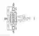
Turning to FIG. 3, an example 300 of a circulator architecture in accordance with some embodiments is shown. As illustrated, circulator 300 includes an antenna port 301, a transmitter port 302, a receiver port 304, a non-reciprocal phase component 306, and transmission lines 308, 310, and 312. Within non-reciprocal phase component 306, there are passive mixers 314, 316, 318, and 320, and transmission lines 322 and 324.
As shown in FIG. 3, values of signals and components in non-reciprocal phase component 306 may depend on an input frequency (ωin) and a modulation frequency (ωm). Win represents the frequency of operation of the circulator. ωm represents the frequency at which the mixers are modulated. Any suitable frequencies can be used for ωin and ωm, in some embodiments. For example, in some embodiments, RF/millimeter-wave/Terahertz frequencies can be used. In some embodiments, ωin and ωm may be required to be sized relative to each other. For example, in some embodiments, the mixing signals at ωin+ωm and ωin−ωm should be 180° out of phase or equivalently the following equation may be required to be met: 2 ωmTd=180°, where Td is the group delay. More particularly, for example, in some embodiments, ωin can be 28 GHz and ωm can be 9.33 GHz.
Each of the transmission lines in FIG. 3 is illustrated as having a “length” that is based on a given frequency. For example, transmission lines 308, 310, and 312 are illustrated as having a length equal to λ/4, where λ is the wavelength for a frequency of ωin. As another example, transmission lines 322 and 324 are illustrated as providing 180° phase difference between the signals at ωin+ωm and ωin−ωm or equivalently a group delay of Td=¼(ωm/2π).
Transmission lines 308, 310, 312, 322, and 324 can be implemented in any suitable manner. For example, in some embodiments, one or more of the transmission lines can be implemented as C-L-C pi-type lumped sections. In some other embodiments, they may be implemented as truly distributed transmission lines.
The passive mixers can be driven by signals as shown in FIG. 3, in some embodiments. For example, in some embodiments, mixer 314 can be driven by a signal cos(ωmt), mixer 316 can be driven by a signal cos(ωmt+ϕ), mixer 318 can be driven by a signal sin(ωmt), and mixer 320 can be driven by a signal sin(ωmt+ϕ), where ϕ is 90° for Td=¼(ωm/2π).
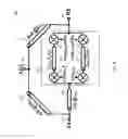
In some embodiments, mixers 314, 316, 318, and 320 shown in FIG. 3 can be implemented with switch groups 414, 416, 418, and 420, respectively, as illustrated in FIG. 4A. As shown in FIG. 4B, the switch groups in FIG. 4A can each include four switches 402, 404, 406, and 408, in some embodiments.
The switches in the switch groups can be implemented in any suitable manner. For example, in some embodiments, the switches can be implemented using NMOS transistors, PMOS transistors, both NMOS and PMOS transistors, or any other suitable transistor or any other switch technology.
Switch groups 414, 416, 418, and 420 can be controlled by local oscillator signals LO1, LO2, LO1Q, and LO2Q, respectively, as shown in FIG. 4A, in some embodiments. A timing diagram showing an example of these signals with respect to each other is shown in FIG. 4C. In this diagram, fLO is equal to ωm/2π. When a local oscillator (e.g., LO1, LO2, LO1Q, or LO2Q) is HIGH, switches 402 and 408 in the corresponding switch group are CLOSED and switches 404 and 406 in the corresponding switch group are OPEN. When a local oscillator (e.g., LO1, LO2, LO1Q, or LO2Q) is LOW, switches 404 and 406 in the corresponding switch group are OPEN and switches 404 and 406 in the corresponding switch group are CLOSED.
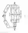
Turning to FIG. 5, an example of a schematic of a circulator that can be implemented in accordance with some embodiments is shown. This circulator is generally in the same architecture as shown in FIG. 3, except that transmission line 308 is split in half and part is place adjacent to the receiver nodes.
Turning to FIG. 6, an example of the architecture of FIG. 3 using 1-stage lattice filters instead of transmission lines 322 and 324 (FIG. 3) is shown. Any suitable filters can be used. For example, in some embodiments, film bulk acoustic resonator (FBAR) filters, surface acoustic wave (SAW) filters, bulk acoustic wave (BAW) filters, and/or any other suitable filters can be used. By implementing large delays using SAW or BAW filters, the clock frequency can be even further reduced. This can be exploited to design even-higher-linearity circulators through the use of high-voltage technologies and high-linearity switch design techniques.
The circuits described herein can be implemented in any suitable technology in some embodiments. For example, in some embodiments, these circuits can be implemented in any semiconductor technology such as silicon, Gallium Nitride (GaN), Indium phosphide (InP), Gallium arsenide (GaAs), etc. More particularly, for example, in some embodiments, the circuits can be implemented in IBM 45 nm SOI CMOS process.
In FIG. 1 the phase shift provided by the non-reciprocal phase component, ϕ−ϕ1, can be tuned by changing the clock phase, ϕ. The frequency at which TX-to-RX isolation is achieved depends on ϕ−ϕ1, so by tuning ϕ, we can tune the isolation frequency.
Although the disclosed subject matter has been described and illustrated in the foregoing illustrative implementations, it is understood that the present disclosure has been made only by way of example, and that numerous changes in the details of implementation of the disclosed subject matter can be made without departing from the spirit and scope of the disclosed subject matter. Features of the disclosed implementations can be combined and rearranged in various ways.
Claims
What is claimed is:1. A circuit, comprising:
a first differential transmission line having: a first end having a first connection a second connection; and a second end having a third connection and a fourth connection;
a first switch having a first side, a second side, and a control, wherein the first side of the first switch is connected to the first connection;
a second switch having a first side, a second side, and a control, wherein the first side of the second switch is connected to the first connection;
a third switch having a first side, a second side, and a control, wherein the first side of the third switch is connected to the second connection and the second side of the third switch is connected to the second side of the first switch;
a fourth switch having a first side, a second side, and a control, wherein the first side of the fourth switch is connected to the second connection and the second side of the fourth switch is connected to the second side of the second switch;
a fifth switch having a first side, a second side, and a control, wherein the first side of the fifth switch is connected to the third connection;
a sixth switch having a first side, a second side, and a control, wherein the first side of the sixth switch is connected to the third connection;
a seventh switch having a first side, a second side, and a control, wherein the first side of the seventh switch is connected to the fourth connection and the second side of the seventh switch is connected to the second side of the fifth switch; and
an eighth switch having a first side, a second side, and a control, wherein the first side of the eighth switch is connected to the fourth connection and the second side of the eighth switch is connected to the second side of the sixth switch.
2. The circuit of claim 1, further comprising:
a second differential transmission line having: a first end having a fifth connection a sixth connection; and a second end having a seventh connection and an eighth connection;
a ninth switch having a first side, a second side, and a control, wherein the first side of the ninth switch is connected to the fifth connection;
a tenth switch having a first side, a second side, and a control, wherein the first side of the tenth switch is connected to the fifth connection;
an eleventh switch having a first side, a second side, and a control, wherein the first side of the eleventh switch is connected to the sixth connection and the second side of the eleventh switch is connected to the second side of the ninth switch;
a twelfth switch having a first side, a second side, and a control, wherein the first side of the twelfth switch is connected to the sixth connection and the second side of the twelfth switch is connected to the second side of the tenth switch;
a thirteenth switch having a first side, a second side, and a control, wherein the first side of the thirteenth switch is connected to the seventh connection;
a fourteenth switch having a first side, a second side, and a control, wherein the first side of the fourteenth switch is connected to the seventh connection;
a fifteenth switch having a first side, a second side, and a control, wherein the first side of the fifteenth switch is connected to the eighth connection and the second side of the fifteenth switch is connected to the second side of the thirteenth switch; and
a sixteenth switch having a first side, a second side, and a control, wherein the first side of the sixteenth switch is connected to the eighth connection and the second side of the sixteenth switch is connected to the second side of the fourteenth switch,
wherein the fifth connection is connected to the first connection, the sixth connection is connected to the second connection, the seventh connection is connected to the third connection, and the eighth connection is connected to the fourth connection.
3. The circuit of claim 1, further comprising:
at least one differential transmission line having a total delay of three quarters of a period of an operating frequency of the circuit, having a first side having a ninth connection and a tenth connection, and having a second side having an eleventh connection and a twelfth connection, wherein the ninth connection is connected to the second side of the first switch, the tenth connection is connected to the second side of the fourth switch, the eleventh connection is connected to the second side of the fifth switch, and the twelfth connection is connected to the second side of the eighth switch.
4. The circuit of claim 3, wherein the at least one differential transmission line comprises:
a third differential transmission line having a delay of one quarter of the period of the operating frequency of the circuit;
a fourth differential transmission line having a delay of one quarter of the period of the operating frequency of the circuit; and
at least one fifth differential transmission line having a total delay of one quarter of the period of the operating frequency of the circuit.
5. The circuit of claim 4, further comprising a transmitter port, an antenna port, and a receiver port, wherein the third differential transmission line is connected between the transmitter port and the antenna port, and the fourth differential transmission line is connected between the antenna port and the receiver port.
6. The circuit of claim 4, wherein the at least one fifth differential transmission line comprises:
a sixth differential transmission line having a delay of one eighth of the period of the operating frequency of the circuit; and
a seventh differential transmission line having a delay of one eighth of the period of the operating frequency of the circuit.
7. The circuit of claim 1, wherein the control of the first switch and the control of the fourth switch are connected to a first local oscillator signal, the control of the second switch and the control of the third switch are connected to a second local oscillator signal, the control of the fifth switch and the control of the eighth switch are connected to a third local oscillator signal, and the control of the sixth switch and the control of the seventh switch are connected to a fourth oscillator signal.
8. The circuit of claim 7, wherein the first oscillator signal and the first oscillator signal and the second oscillator signal are 180 degrees out of phase, the third oscillator signal and the fourth oscillator signal are 180 degrees out of phase, and the third oscillator signal is delay from the first oscillator signal by one quarter of a period of an operating frequency of the circuit.
9. The circuit of claim 8, wherein the first local oscillator, the second local oscillator, the third local oscillator, and the fourth local oscillator each have a 50% duty cycle.
10. The circuit of claim 1, wherein the first differential transmission line has a delay of one quarter of a period of an operating frequency of the circuit.
11. The circuit of claim 1, wherein the first differential transmission line is implemented as at least one C-L-C pi-type lumped section.
Images & Drawings included:


Sources:
- United States Patent and Trademark Office - verify current appl. status at the USPTO↗
Similar patent applications:
Recent applications in this class:
- » 20240339744 2024-10-10
Circulator Arrangement and Means of Construction for a Microwave Oven - » 20240113407 2024-04-04
Integrated thick film spacer for RF devices - » 20240079753 2024-03-07
Fabrication of surface mount microstrip circulators using a ferrite and ceramic dielectric assembly substrate - » 20230125826 2023-04-27
CIRCULATOR DESIGN AND METHODS OF FABRICATING THE CIRCULATOR - » 20230112914 2023-04-13
LOW-LOSS QUASI-CIRCULATOR - » 20220416390 2022-12-29
Double-disc structure for self-biased circulators monolithically integrated on semiconductors - » 20220231393 2022-07-21
Integrated thick film spacer for RF devices - » 20220181760 2022-06-09
Surface mount microstrip circulators using a ferrite and ceramic dielectric assembly substrate - » 20210384599 2021-12-09
Reconfigurable wideband high-frequency filter using non-reciprocal circulator - » 20210384598 2021-12-09
Reconfigurable wideband high-frequency circuits using non-reciprocal circulators
Recent applications for this Assignee:
- » 20250290113 2025-09-18
MODIFIED BACTERIAL PROTEIN EXPRESSION SYSTEM - » 20250284135 2025-09-11
Four-Way Image Splitter for High-Speed Characterization of Tissue Samples - » 20250278625 2025-09-04
VISUOMOTOR POLICY LEARNING VIA ACTION DIFFUSION - » 20250277800 2025-09-04
NUCLEIC ACID SEQUENCES RESPONSIVE TO CREATININE IN CLINICALLY USEFUL RANGES - » 20250273228 2025-08-28
Systems and Methods for Enhancing Auditory Attention Decoding Using Spatial Cues - » 20250270385 2025-08-28
DYNAMICALLY CROSSLINKED MULTIBLOCK COPOLYMERS FOR COMPATIBILIZING IMMISCIBLE MIXED PLASTICS - » 20250264398 2025-08-21
Systems and Methods for Identifying and Recovering Rare Biological Cells from a Sample - » 20250255976 2025-08-14
CATIONIC BIOMATERIALS AMELIORATE OBESITY-ASSOCIATED CHRONIC INFLAMMATION AND FOCAL ADIPOSITY - » 20250252263 2025-08-07
Systems and Methods for Detecting Generated Text Through Rewriting Operations - » 20250243537 2025-07-31
SYNTHESIS OF CLEAVABLE FLUORESCENT NUCLEOTIDES AS REVERSIBLE TERMINATORS FOR DNA SEQUENCING BY SYNTHESIS