Capacitor-coupled N-type transistor-based one-time programmable device
US20200020706A1
2020-01-16
16/202,636
2018-11-28
✅ Patent granted
US 10,679,999 B2
2020-06-09
-
-
Tu-Tu V Ho
Murtha Cullina LLP
2038-11-28
Abstract:
A capacitor-coupled N-type transistor-based one-time programmable (OTP) device is disclosed. The OTP includes a transistor and a coupling capacitor both formed in a p-well and isolated from each other by field oxide or shallow trench isolation (STI). The transistor is constructed of a gate, a source region and a drain region composed of heavily-doped N-region. The coupling capacitor has a top plat formed of polysilicon on substrate surface, and a bottom plate constructed of an NLDD region and a heavily-doped N-region in the NLDD region. In order to achieve maximum capacitance utilization, the top plate of the coupling capacitor has a width not greater than the NLDD implantation region or twice a lateral junction depth of the heavily-doped n-region. The gate of the transistor may not be wider than the top plate of the coupling capacitor such that capacitance coupling ratio of the coupling capacitor to the transistor is optimized.
Inventors:
- Yu Chen 145 🇨🇳 Shanghai, China
- Yuan Yuan 15 🇨🇳 Shanghai, China
- Hualun CHEN 3 🇨🇳 Shanghai, China
Assignee:
- Shanghai Huahong Grace Semiconductor Manufacturing Corporation 138 🇨🇳 Shanghai, China
Applicant:
Interested in similar patents?
Get notified when new applications in this technology area are published.
Classification:
H01L27/11206 » CPC main
Devices consisting of a plurality of semiconductor or other solid-state components formed in or on a common substrate including semiconductor components specially adapted for rectifying, oscillating, amplifying or switching and having at least one potential-jump barrier or surface barrier; including integrated passive circuit elements with at least one potential-jump barrier or surface barrier the substrate being a semiconductor body including a plurality of individual components in a repetitive configuration including field-effect components; Read-only memory structures [ROM] and multistep manufacturing processes therefor Programmable ROM [PROM], e.g. memory cells comprising a transistor and a fuse or an antifuse
H01L23/5256 » CPC further
Details of semiconductor or other solid state devices; Arrangements for conducting electric current within the device in operation from one component to another, i.e. interconnections, e.g. wires, lead frames including external interconnections consisting of a multilayer structure of conductive and insulating layers inseparably formed on the semiconductor body with adaptable interconnections comprising fuses, i.e. connections having their state changed from conductive to non-conductive
H01L28/60 » CPC further
Passive two-terminal components without a potential-jump or surface barrier for integrated circuits; Details thereof; Multistep manufacturing processes therefor; Capacitors Electrodes
H01L29/0649 » CPC further
Semiconductor devices adapted for rectifying, amplifying, oscillating or switching, or capacitors or resistors with at least one potential-jump barrier or surface barrier, e.g. PN junction depletion layer or carrier concentration layer; Details of semiconductor bodies or of electrodes thereof; Multistep manufacturing processes therefor; Semiconductor bodies ; Multistep manufacturing processes therefor characterised by their shape; characterised by the shapes, relative sizes, or dispositions of the semiconductor regions ; characterised by the concentration or distribution of impurities within semiconductor regions characterised by particular constructional design considerations, e.g. for preventing surface leakage, for controlling electric field concentration or for internal isolations regions; Isolation within the component, i.e. internal isolation Dielectric regions, e.g. SiO regions, air gaps
H01L27/112 IPC
Devices consisting of a plurality of semiconductor or other solid-state components formed in or on a common substrate including semiconductor components specially adapted for rectifying, oscillating, amplifying or switching and having at least one potential-jump barrier or surface barrier; including integrated passive circuit elements with at least one potential-jump barrier or surface barrier the substrate being a semiconductor body including a plurality of individual components in a repetitive configuration including field-effect components Read-only memory structures [ROM] and multistep manufacturing processes therefor
H01L21/265 IPC
Processes or apparatus adapted for the manufacture or treatment of semiconductor or solid state devices or of parts thereof; Manufacture or treatment of semiconductor devices or of parts thereof the devices having at least one potential-jump barrier or surface barrier, e.g. PN junction, depletion layer or carrier concentration layer the devices having semiconductor bodies comprising elements of Group IV of the Periodic System or AB compounds with or without impurities, e.g. doping materials; Bombardment with radiation with high-energy radiation producing ion implantation
H01L23/525 IPC
Details of semiconductor or other solid state devices; Arrangements for conducting electric current within the device in operation from one component to another, i.e. interconnections, e.g. wires, lead frames including external interconnections consisting of a multilayer structure of conductive and insulating layers inseparably formed on the semiconductor body with adaptable interconnections
H01L29/06 IPC
Semiconductor devices adapted for rectifying, amplifying, oscillating or switching, or capacitors or resistors with at least one potential-jump barrier or surface barrier, e.g. PN junction depletion layer or carrier concentration layer; Details of semiconductor bodies or of electrodes thereof; Multistep manufacturing processes therefor; Semiconductor bodies ; Multistep manufacturing processes therefor characterised by their shape; characterised by the shapes, relative sizes, or dispositions of the semiconductor regions ; characterised by the concentration or distribution of impurities within semiconductor regions
H01L49/02 IPC
Solid state devices not provided for in groups - and and not provided for in any other subclass; Processes or apparatus peculiar to the manufacture or treatment thereof or of parts thereof Thin-film or thick-film devices
Description
CROSS-REFERENCE TO RELATED APPLICATION
This application claims the priority of Chinese patent application number 201810757171.7, filed on Jul. 11, 2018, the entire contents of which are incorporated herein by reference.
TECHNICAL FIELD
The present invention relates to the field of semiconductor devices and, in particular, to a capacitor-coupled N-type transistor-based one-time programmable (OTP) device.
BACKGROUND
Existing capacitor-coupled N-type transistor-based OTP devices can be categorized primarily into the following three types.
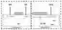
The first type of OTP device is shown in FIG. 1, which includes a transistor (depicted on the left) and a capacitor (depicted on the right). The transistor is formed in a P-well and has NLDD structures. The capacitor is in an N-well and has a PLDD structure. Source and drain doping of such a transistor is the same as that for an ordinary NMOS transistor. The capacitor has a bottom plate consisting of the N-well as well as of a heavily-doped P-region. This OTP device is, however, disadvantageous in that: since the transistor is sized at approximately 80% of an ordinary device, but has the same source and drain doping as an ordinary device, its efficiency and time window for hot carrier writing are limited. Moreover, the capacitor must have a relatively large area due to the size of the N-well of its bottom plate.
The second type of OTP device is shown in FIG. 2, which includes a transistor (depicted on the left) and a capacitor (depicted on the right), both formed in the same P-well. The transistor has NLDD structures, and the capacitor has a bulky N-doped region. Similarly, source and drain doping of the transistor is the same as that for an ordinary NMOS transistor. Additionally, the capacitor has a bottom plate formed by an additional N-type implantation. This OTP device is, however, disadvantageous in that: since the transistor is sized at approximately 80% of an ordinary device, but has the same source and drain doping as an ordinary device, its efficiency and time window for hot carrier writing are limited. Moreover, it requires an additional N-type implantation.
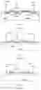
The third type of OTP device is shown in FIG. 3, which includes a transistor (depicted on the left) and a capacitor (depicted on the right), both formed in the same P-well. Each of the transistor and the capacitor has NLDD structure(s). Similarly, source and drain doping of the transistor is the same as that for an ordinary NMOS transistor. The capacitor has a bottom plate formed by a heavily-doped N-region stacked with a coupling capacitor. This OTP device is, however, disadvantageous in that: since the transistor is sized at approximately 80% of an ordinary device, but has the same source and drain doping as, an ordinary device, its efficiency and time window for hot carrier writing are limited. Moreover, the capacitor has a low coupling ratio and a large area.
SUMMARY OF THE INVENTION
It is an object of the present invention to provide a capacitor-coupled N-type transistor-based one-time programmable (OTP) device
This object is attained by a capacitor-coupled N-type transistor-based OTP device according to the present invention, comprising a transistor and a coupling capacitor both located in a P-well and isolated from each other by a field oxide or a shallow trench isolation (STI), the transistor comprising a gate, a source region, and a drain region, the source and drain regions each composed of a heavily-doped N-region, the coupling capacitor having a top plate formed by a polysilicon on a substrate surface, and a bottom plate formed by an NLDD implantation region and a heavily-doped N-region in the NLDD implantation region.
Additionally, the gate of the transistor and the top plate of the coupling capacitor may be formed by etching the same polysilicon layer.
Additionally, the bottom plate may either be independently dedicated to the coupling capacitor of each cell or an active region of coupling capacitors of multiple cells may be joined.
Additionally, the top plate of the coupling capacitor may have a width not greater than twice an overlapping lateral width of the NLDD implantation region and an overlying gate so that a capacitance utilization efficiency is maximized.
Additionally, the gate of the transistor may have a width not greater than a width of the top plate of the coupling capacitor such that a capacitance coupling ratio of the coupling capacitor to the transistor is optimized.
Additionally, an ion-implantation process for forming the heavily-doped N-region may comprise an implantation of N-type ions conducted at an inclination angle of 15 to 45 degrees to form an effective connection between the source and the drain as well as to optimize a hot carrier writing efficiency.
In the capacitor-coupled N-type transistor-based OTP device of the present invention, the bottom plate of the coupling capacitor is formed by an NLDD region and a heavily-doped n-region, and may either be independently dedicated to the coupling capacitor of each cell or common to coupling capacitors in multiple cells. The doped source and drain do not contain an NLDD region. In the OTP device of the present invention, the width of the polysilicon gate in the coupling capacitor and the transistor is reduced to about half that of an ordinary MOS device produced by the same process, resulting in area shrinkage of corresponding memory cells, while not requiring any additional photolithography step.
BRIEF DESCRIPTION OF THE DRAWINGS
FIGS. 1 to 3 are conventional capacitor-coupled N-type transistor-based OTP devices of three distinct structures.
FIG. 4 is a schematic diagram of a capacitor-coupled N-type transistor-based OTP device constructed in accordance with the present invention.
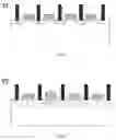
FIG. 5 shows the layout of a capacitor-coupled N-type transistor-based OTP device constructed in accordance with the present invention.
FIG. 6 is a cross-sectional view taken along the line Y1 in FIG. 5.
FIG. 7 is a cross-sectional view taken along the line Y2 in FIG. 5.
DETAILED DESCRIPTION
As shown in FIG. 4, a capacitor-coupled N-type transistor-based one-time programmable (OTP) device embodying the present invention includes a transistor and a coupling capacitor, both located in a P-well. The transistor is isolated from the coupling capacitor by a field oxide or a shallow trench isolation (STI) (as in the case of FIG. 4). The transistor is comprised of a gate G a source region S and a drain region D. Each of the source and drain regions is formed of a heavily-doped N-region. A top plate of the coupling capacitor is formed of a polysilicon on a substrate surface. A bottom plate of the coupling capacitor is formed of an N-type lightly-doped drain (NLDD) implantation region and a heavily-doped N-region in the NLDD region. The NLDD region may laterally extend from the STI to another adjacent STI such that the NLDD region substantially spans the whole lateral width of the top plate. In case of an array of such OTP devices formed in the substrate, in every adjacent two devices in the array, active regions of the coupling capacitors may be either joined together or independent from each other.
The gate of the transistor and the top plate of the coupling capacitor may be formed by etching the same single layer of polysilicon.
FIG. 5 shows the layout of an OTP device embodying the present invention, in which two directions Y1 and Y2 are shown. FIG. 6 is a cross-sectional view taken along the line Y1 in FIG. 5, showing a column of transistors. FIG. 7 is a cross-sectional view taken along the line Y2 in FIG. 5, showing a column of coupling capacitors. As shown in FIG. 7, in order to maximize capacitance utilization efficiency, the top plate of the coupling capacitor may have a width m that is not greater than twice an overlapping lateral width n of the NLDD region and an overlying gate (n also could be understood as twice a lateral junction depth of the heavily-doped N-region).
As shown in FIG. 4, in order to achieve an optimized capacitance coupling ratio of the coupling capacitor to the transistor, the gate of the transistor may not be wider than the top plate of the coupling capacitor.
An ion-implantation process for forming the heavily-doped N-region in the transistor may involve an N-type implantation in a direction pointing toward the gate region and being inclined at an angle of 15 to 45 degrees with respect to the vertical direction, which ensures an effective connection between the source and drain regions, and optimizes a hot carrier writing efficiency.
The OTP device of the present invention may be fabricated using a process including the steps of:
1. defining an active region by a LOCOS or STI process;
2. forming the P-well, as well as an N-well for the remaining circuit part, by photolithography and ion-implantation;
3. depositing polysilicon on the substrate surface, and forming the polysilicon gate of the transistor and the top plate of the coupling capacitor by photolithography and plasma etching, wherein the gate and the top plate are formed by a single etching process;
4. forming the NLDD region of the coupling capacitor by photolithography and ion implantation, wherein the NLDD implantation is only applied to the area of the bottom plate of the coupling capacitor but not applied to the area of the transistor;
5. forming a spacer in a CMOS device in the circuit;
6. forming heavily-doped N-regions by photolithography and ion implantation, such that heavily-doped N-regions are formed both in the source and drain regions of the transistor and in the bottom plate of the coupling capacitor;
7. forming a heavily-doped P-region by photolithography and ion implantation, which serves for external connection of the P-well, and performing source and drain doping for other PMOS devices in the circuit;
8. forming a silicide; and
9. forming back-end interconnections and a passivation layer by using CMOS process and ending this fabrication process.
While the invention has been described above with reference to several preferred embodiments, its scope is in no way limited to these embodiments. For those skilled in the art, various modifications and changes are also possible to the invention. Any and all variations, equivalent substitutions, modifications and the like made without departing from the spirit and scope of the present invention are intended to be embraced within the scope thereof.
Claims
What is claimed is:1. A capacitor-coupled N-type transistor-based one-time programmable (OTP) device, comprising a transistor and a coupling capacitor both located in a P-well and isolated from each other by a field oxide or a shallow trench isolation, the transistor comprising a gate, a source region and a drain region, the source and drain regions each composed of a heavily-doped N-region, the coupling capacitor having a top plate formed by a polysilicon on a substrate surface, and a bottom plate formed by an NLDD implantation region and a heavily-doped N-region in the NLDD implantation region.
2. The OTP device of claim 1, wherein the gate of the transistor and the top plate of the coupling capacitor are formed by etching a same polysilicon layer.
3. The OTP device of claim 1, comprising a plurality of cells arranged in an array, each cell comprising one transistor and one corresponding coupling capacitor, wherein in every two adjacent ones of the cells, the bottom plates of the coupling capacitors are independent from each other.
4. The OTP device of claim 1, comprising a plurality of cells arranged in an array, each cell comprising one transistor and one corresponding coupling capacitor, wherein in every two adjacent ones of the cells, active regions of the coupling capacitors are joined together.
5. The OTP device of claim 1, wherein the top plate of the coupling capacitor has a width not greater than twice an overlapping lateral width of the NLDD implantation region and an overlying gate so that a capacitance utilization efficiency is maximized.
6. The OTP device of claim 1, wherein the gate of the transistor has a width not greater than a width of the top plate of the coupling capacitor so that a capacitance coupling ratio of the coupling capacitor to the transistor is optimized.
7. The OTP device of claim 1, wherein an ion-implantation process for forming the heavily-doped N-region comprises an implantation of N-type ions conducted at an inclination angle of 15 to 45 degrees to form an effective connection between the source and the drain as well as to optimize a hot carrier writing efficiency.
Images & Drawings included:

Sources:
- United States Patent and Trademark Office - verify current appl. status at the USPTO↗
Recent applications in this class:
- » 20240188287 2024-06-06
ONE-TIME PROGRAMMABLE FUSE USING PN JUNCTION OVER GATE METAL LAYER, AND RELATED METHOD - » 20240164089 2024-05-16
BACKSIDE PROGRAMMABLE MEMORY - » 20240114682 2024-04-04
WRAP-AROUND MEMORY CIRCUIT - » 20240090208 2024-03-14
SEMICONDUCTOR STRUCTURE - » 20240074168 2024-02-29
MEMORY DEVICES HAVING ONE-TIME-PROGRAMMABLE FUSES AND/OR ANTIFUSES FORMED FROM THIN-FILM TRANSISTORS - » 20240074167 2024-02-29
ELECTRICALLY PROGRAMMABLE FUSE OVER LATERAL BIPOLAR TRANSISTOR - » 20240040779 2024-02-01
ANTIFUSE, APPARATUS, AND METHOD OF FORMING THE SAME - » 20240023326 2024-01-18
MULTI-STACK NANOSHEET STRUCTURE INCLUDING SEMICONDUCTOR DEVICE - » 20240008269 2024-01-04
MEMORY DEVICE AND METHOD OF FORMING THE SAME - » 20230422492 2023-12-28
SEMICONDUCTOR STRUCTURE AND METHOD FOR MANUFACTURING SAME, MEMORY AND OPERATION METHOD THEREOF
Recent applications for this Assignee:
- » 20250176290 2025-05-29
PHOTOSENSITIVE DEVICE AND FORMING METHOD THEREFOR - » 20250176185 2025-05-29
SONOS STRUCTURE, METHOD FOR PROGRAMMING THE SAME AND METHOD FOR FORMING THE SAME, AND MEMORY - » 20250081455 2025-03-06
Semiconductor Structure and Method for Forming the Same - » 20230354598 2023-11-02
Memory and Method for Forming the Same - » 20230337425 2023-10-19
Memory Structure And Method For Forming The Same - » 20230269945 2023-08-24
EMBEDDED SONOS MEMORY AND METHOD OF MAKING THE SAME - » 20230268000 2023-08-24
Memory array - » 20230112037 2023-04-13
Semiconductor Structure and Method of Forming the Same - » 20230101771 2023-03-30
IGBT device and method of making the same - » 20230085878 2023-03-23
HIGH-VOLTAGE ISOLATION SEMICONDUCTOR DEVICE AND METHOD OF MAKING THE SAME