Asymmetric transient voltage suppressor device and methods for formation
US20200035673A1
2020-01-30
16/589,452
2019-10-01
✅ Patent granted
US 10,957,692 B2
2021-03-23
-
-
Davienne N Monbleau | Scott R Wilson
Kacvinsky Daisak Bluni PLLC
2039-10-01
Abstract:
A transient voltage suppression (TVS) device, may include: a substrate base formed in a substrate, the substrate base comprising a semiconductor of a first conductivity type; and an epitaxial layer, disposed on the substrate base, on a first side of the substrate, and comprising a semiconductor of a second conductivity type. The epitaxial layer may include: a first portion, the first portion having a first layer thickness; and a second portion, the second portion having a second layer thickness, less than the first layer thickness, wherein the first portion and the second portion are disposed on a first side of the substrate, and wherein the first portion is electrically isolated from the second portion.
Assignee:
- LITTELFUSE, INC. 432 🇺🇸 Chicago, IL, United States
Applicant:
Interested in similar patents?
Get notified when new applications in this technology area are published.
Classification:
H01L27/0814 » CPC main
Devices consisting of a plurality of semiconductor or other solid-state components formed in or on a common substrate including semiconductor components specially adapted for rectifying, oscillating, amplifying or switching and having at least one potential-jump barrier or surface barrier; including integrated passive circuit elements with at least one potential-jump barrier or surface barrier the substrate being a semiconductor body including only semiconductor components of a single kind Diodes only
H01L23/49551 » CPC further
Details of semiconductor or other solid state devices; Arrangements for conducting electric current to or from the solid state body in operation, e.g. leads, terminal arrangements ; Selection of materials therefor consisting of soldered constructions; Lead-frames or other flat leads; Geometry of the lead-frame; Cross section geometry characterised by bent parts
H01L23/49562 » CPC further
Details of semiconductor or other solid state devices; Arrangements for conducting electric current to or from the solid state body in operation, e.g. leads, terminal arrangements ; Selection of materials therefor consisting of soldered constructions; Lead-frames or other flat leads; Geometry of the lead-frame for devices being provided for in
H01L29/0661 » CPC further
Semiconductor devices adapted for rectifying, amplifying, oscillating or switching, or capacitors or resistors with at least one potential-jump barrier or surface barrier, e.g. PN junction depletion layer or carrier concentration layer; Details of semiconductor bodies or of electrodes thereof; Multistep manufacturing processes therefor; Semiconductor bodies ; Multistep manufacturing processes therefor characterised by their shape; characterised by the shapes, relative sizes, or dispositions of the semiconductor regions ; characterised by the concentration or distribution of impurities within semiconductor regions characterised by the shape of the body specially adapted for altering the breakdown voltage by removing semiconductor material at, or in the neighbourhood of, a reverse biased junction, e.g. by bevelling, moat etching, depletion etching
H01L23/495 IPC
Details of semiconductor or other solid state devices; Arrangements for conducting electric current to or from the solid state body in operation, e.g. leads, terminal arrangements ; Selection of materials therefor consisting of soldered constructions Lead-frames or other flat leads
H01L29/0649 » CPC further
Semiconductor devices adapted for rectifying, amplifying, oscillating or switching, or capacitors or resistors with at least one potential-jump barrier or surface barrier, e.g. PN junction depletion layer or carrier concentration layer; Details of semiconductor bodies or of electrodes thereof; Multistep manufacturing processes therefor; Semiconductor bodies ; Multistep manufacturing processes therefor characterised by their shape; characterised by the shapes, relative sizes, or dispositions of the semiconductor regions ; characterised by the concentration or distribution of impurities within semiconductor regions characterised by particular constructional design considerations, e.g. for preventing surface leakage, for controlling electric field concentration or for internal isolations regions; Isolation within the component, i.e. internal isolation Dielectric regions, e.g. SiO regions, air gaps
H01L2924/181 » CPC further
Indexing scheme for arrangements or methods for connecting or disconnecting semiconductor or solid-state bodies as covered by; Details of package parts other than the semiconductor or other solid state devices to be connected Encapsulation
H01L27/08 IPC
Devices consisting of a plurality of semiconductor or other solid-state components formed in or on a common substrate including semiconductor components specially adapted for rectifying, oscillating, amplifying or switching and having at least one potential-jump barrier or surface barrier; including integrated passive circuit elements with at least one potential-jump barrier or surface barrier the substrate being a semiconductor body including only semiconductor components of a single kind
H01L29/861 » CPC further
Semiconductor devices adapted for rectifying, amplifying, oscillating or switching, or capacitors or resistors with at least one potential-jump barrier or surface barrier, e.g. PN junction depletion layer or carrier concentration layer; Details of semiconductor bodies or of electrodes thereof; Multistep manufacturing processes therefor; Types of semiconductor device ; Multistep manufacturing processes therefor controllable only by variation of the electric current supplied, or only the electric potential applied, to one or more of the electrodes carrying the current to be rectified, amplified, oscillated or switched Diodes
H01L29/06 IPC
Semiconductor devices adapted for rectifying, amplifying, oscillating or switching, or capacitors or resistors with at least one potential-jump barrier or surface barrier, e.g. PN junction depletion layer or carrier concentration layer; Details of semiconductor bodies or of electrodes thereof; Multistep manufacturing processes therefor; Semiconductor bodies ; Multistep manufacturing processes therefor characterised by their shape; characterised by the shapes, relative sizes, or dispositions of the semiconductor regions ; characterised by the concentration or distribution of impurities within semiconductor regions
H01L29/66136 » CPC further
Semiconductor devices adapted for rectifying, amplifying, oscillating or switching, or capacitors or resistors with at least one potential-jump barrier or surface barrier, e.g. PN junction depletion layer or carrier concentration layer; Details of semiconductor bodies or of electrodes thereof; Multistep manufacturing processes therefor; Types of semiconductor device ; Multistep manufacturing processes therefor; Multistep manufacturing processes of devices having semiconductor bodies comprising group 14 or group 13/15 materials the devices being controllable only by variation of the electric current supplied or the electric potential applied, to one or more of the electrodes carrying the current to be rectified, amplified, oscillated or switched, e.g. two-terminal devices; Diodes PN junction diodes
H01L29/8613 » CPC further
Semiconductor devices adapted for rectifying, amplifying, oscillating or switching, or capacitors or resistors with at least one potential-jump barrier or surface barrier, e.g. PN junction depletion layer or carrier concentration layer; Details of semiconductor bodies or of electrodes thereof; Multistep manufacturing processes therefor; Types of semiconductor device ; Multistep manufacturing processes therefor controllable only by variation of the electric current supplied, or only the electric potential applied, to one or more of the electrodes carrying the current to be rectified, amplified, oscillated or switched; Diodes Mesa PN junction diodes
H01L29/66 IPC
Semiconductor devices adapted for rectifying, amplifying, oscillating or switching, or capacitors or resistors with at least one potential-jump barrier or surface barrier, e.g. PN junction depletion layer or carrier concentration layer; Details of semiconductor bodies or of electrodes thereof; Multistep manufacturing processes therefor Types of semiconductor device ; Multistep manufacturing processes therefor
Description
CROSS-REFERENCE
This application is a divisional of, and claims priority to, pending U.S. non-provisional patent application Ser. No. 15/816,115, filed Nov. 17, 2017, the entirety of which application is incorporated by reference herein.
BACKGROUND
Field
Embodiments relate to the field of circuit protection devices, including fuse devices.
Discussion of Related Art
Semiconductor devices such as transient voltage suppressor (TVS) devices may be fabricated as unidirectional devices or bidirectional devices. In the case of bidirectional devices, a first device may be fabricated on a first side of a semiconductor die (chip), while a second device may be fabricated on a second side of the semiconductor die. Bidirectional devices may include symmetric devices where the first device and second device are the same, as well as asymmetric devices, where the first device and second device differ in properties.
While such bidirectional devices provide some flexibility in designing electrical properties of the different devices on different sides of a semiconductor die, the packaging of such devices may be relatively complex.
With respect to these and other considerations, the present disclosure is provided.
SUMMARY
Exemplary embodiments are directed to improved TVS devices and techniques for forming TVS devices.
In one embodiment, a transient voltage suppression (TVS) device may include a substrate base formed in a substrate, the substrate base comprising a semiconductor of a first conductivity type; and an epitaxial layer, disposed on the substrate base, on a first side of the substrate, and comprising a semiconductor of a second conductivity type. The epitaxial layer may include: a first portion, the first portion having a first layer thickness; and a second portion, the second portion having a second layer thickness, less than the first layer thickness, wherein the first portion and the second portion are disposed on a first side of the substrate, and wherein the first portion is electrically isolated from the second portion.
In another embodiment, a transient voltage suppression (TVS) device assembly may include a TVS device, where the TVS device includes a substrate base formed in a substrate, the substrate base comprising a semiconductor of a first conductivity type. The TVS device may include an epitaxial layer, disposed on the substrate base, on a first side of the epitaxial layer comprising a semiconductor of a second conductivity type. The epitaxial layer may further include a first portion, the first portion having a first layer thickness; and a second portion, the second portion having a second layer thickness, less than the first layer thickness, wherein the second portion comprises a trench shape, wherein a plane defined by a first upper surface of the first portion is above a second upper surface of the second portion. The TVS device assembly may also include a leadframe, the leadframe being coupled to the TVS device, the leadframe comprising: a first part, the first part being connected to the first portion of the TVS device; and a second part, the second part being coupled to the second portion of the TVS device.
In another embodiment, a method may include providing a substrate having a base layer of a first conductivity type; forming an epitaxial layer of a second conductivity type on the base layer, wherein the epitaxial layer is disposed on a first side of the substrate; forming a first epitaxial portion and a second epitaxial portion within the epitaxial layer, wherein the first epitaxial portion is electrically isolated from the second epitaxial portion; forming a recess within the second epitaxial portion, wherein the first diode and the second diode are formed within the epitaxial layer on the first side of the substrate.
BRIEF DESCRIPTION OF THE DRAWINGS
FIG. 1 illustrates a TVS device according to embodiments of the disclosure;
FIG. 2 illustrates a TVS device assembly according to other embodiments of the disclosure;
FIG. 3 depicts an exemplary process flow according to embodiments of the disclosure.
DESCRIPTION OF EMBODIMENTS
The present embodiments will now be described more fully hereinafter with reference to the accompanying drawings, in which exemplary embodiments are shown. The embodiments are not to be construed as limited to the embodiments set forth herein. Rather, these embodiments are provided so that this disclosure will be thorough and complete, and will fully convey their scope to those skilled in the art. In the drawings, like numbers refer to like elements throughout.
In the following description and/or claims, the terms “on,” “overlying,” “disposed on” and “over” may be used in the following description and claims. “On,” “overlying,” “disposed on” and “over” may be used to indicate that two or more elements are in direct physical contact with one another. Also, the term “on,”, “overlying,” “disposed on,” and “over”, may mean that two or more elements are not in direct contact with one another. For example, “over” may mean that one element is above another element while not contacting one another and may have another element or elements in between the two elements.
In various embodiments, novel device structures and techniques are provided for forming a bidirectional TVS device.
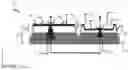
FIG. 1 illustrates a TVS device 100 according to embodiments of the disclosure. The TVS device 100 may include a substrate base 102 formed in a substrate 101. The substrate base 102 may be formed of a semiconductor of a first conductivity type, such as a P-type semiconductor. The TVS device 100 may further include an epitaxial layer 104, disposed on the substrate base 102, on a first side of the substrate 101 (top side in FIG. 1) as shown. The epitaxial layer 104 may be formed of a semiconductor of a second conductivity type. For example, when the substrate base 102 is P-type silicon, the epitaxial layer may be N-type silicon. For example, when the substrate base 102 is N-type silicon, the epitaxial layer may be P-type silicon. As such, a P/N junction may be formed at the interface between the substrate base 102 and epitaxial layer 104. The epitaxial layer 104 may further comprise a first portion 106 and a second portion 108. The first portion 106 may have a first layer thickness, while the second portion 108 may have a second layer thickness, less than the first layer thickness. As shown, the first portion 106 and the second portion 108 are disposed on the first side of the substrate 101. The first portion 106 is electrically isolated from the second portion 108, by virtue of an isolation structure 110. As shown, the isolation structure 110 extends from the surface of the first side of the substrate 101 into the substrate base 102. The isolation structure 110 may be formed in a known manner, such as using a trench insulator.
As such, the first portion 106 forms a first diode 118, in conjunction with the substrate base 102. As such, the second portion 108 forms a second diode 120, in conjunction with the substrate base 102. According to various embodiments of the disclosure, the first diode differs from the second diode in breakdown voltage, power capacity, or breakdown voltage and power capacity. For example, by virtue of the second portion 108 of the epitaxial layer 104 having a relatively lesser thickness as compared to the first portion 106, the breakdown voltage of the second portion 108 may be lower as compared to the breakdown voltage of the first portion 106. For example, the first layer thickness of the first portion 106 may be between 20 μm and 80 μm in some embodiments, while for a given first layer thickness of the first portion 106, the second layer thickness of the second portion 108 may be less than the given first layer thickness.
As further shown in FIG. 1, the first diode 118 and the second diode 120, formed within the substrate 101, are arranged in electrical series in an anode-to-anode configuration. The respective cathodes of the first diode 118 and the second diode 120 may be electrically contacted through contact 114 and contact 116, respectively, formed on the first side of the substrate 101. As such, the TVS device 100 may form an asymmetric single sided bi-directional device.
The degree of voltage asymmetry between the first diode 118 and the second diode 120 may be arranged by adjusting the relative thickness of the first layer thickness of first portion 106 as compared to the second layer thickness of the second portion 108. For example, in various embodiments, the epitaxial layer 104 is formed as a blanket layer on the substrate base 102, so the dopant level is uniform across the epitaxial layer 104. While the first portion 106 may remain unaltered, after the initial formation of the epitaxial layer 104 with a uniform thickness, the second portion 108 may be etched to reduce the layer thickness of the second portion 108. For example, the second portion 108 may be selectively etched by masking the first portion 106 while subjecting the second portion 108 to a known etchant, forming a recess or a trench shape, as shown by the trench 112. In the example of FIG. 1, a plane 122 defined by a first upper surface 124 of the first portion 106 is above a second upper surface 126 of the second portion 108.
The second portion 108 may be etched to form a uniform, second layer thickness over most of the area (within the plane of the substrate 101) of the second portion 108, such as 80% of the area, 90% of the area, 99% of the area, and so forth. In this manner, the second portion 108 may be etched to a target average layer thickness to adjust the breakdown voltage of the second diode 120 to be different from the breakdown voltage of the first diode 118. Because the first portion 106 and the second portion 108 may have the same active dopant concentration, the different breakdown voltage to be imparted to the second diode 120 may be readily adjusted to a target value by etching a target amount of the second portion to reach a target thickness. For example, if the first diode 118 is formed with a first layer thickness of 60 μm and a breakdown voltage of 600 V, the second diode 120 may be formed by etching to yield a second layer thickness of the second portion 108 of 30 μm, in order to yield a breakdown voltage of much less than 600 V.
The above example of voltage asymmetry between first diode 118 and second diode 120 is merely exemplary while the embodiments are not limited in this context. In various additional embodiments, the first diode 118 may comprise a breakdown voltage of 300 V or greater, and while the second diode 120 comprises a breakdown voltage of 100 V or less. Again, the embodiments are not limited in this context.
In other embodiments, where the first diode 118 and second diode 120 exhibit asymmetry in power capacity, the first diode 118 may comprise a power capacity of 700 W or greater, and the second diode may comprise a power capacity of 500 W or less. The power capacity of the first diode 118 and second diode 120 may be set to be different from one another. The power capacity may be adjusted by adjusting the areas of the first portion 106 and the second portion 108 within the plane (X-Y plane of the Cartesian coordinate system shown) of the substrate 101. The areas may be adjusted by forming masks of different sizes to define the first portion 106 and second portion 108, according to known techniques in the art.
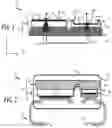
An advantage of the design of FIG. 1 for an asymmetric device is that a leadframe may be attached to just one side of the substrate 101, in order to contact the different diodes. FIG. 2 illustrates a TVS device assembly 150. The TVS device assembly 150 may include the TVS device 100 and leadframe 160, where the leadframe 160 contacts the first surface of the TVS device 100, meaning the upper surface of FIG. 1. In this example, the leadframe 160 may include a first part 162, where the first part 162 is connected to the first portion 106 of the TVS device 100, and may include a second part 164, coupled to the second portion 108 of the TVS device 100. In the example of FIG. 2 the TVS assembly includes a housing 170, which housing may be a molded package. The leadframe 160 may be conveniently attached to the TVS device 100 by soldering or other bonding method.
FIG. 3 depicts an exemplary process flow 300 according to embodiments of the disclosure. At block 302, a substrate is provided, where the substrate includes a base layer of a first conductivity type. The substrate may be, for example, a p-type silicon substrate where the base layer represents the substrate itself. At block 304, an epitaxial layer of a second conductivity type is formed on the base layer, wherein the epitaxial layer is disposed on a first side of the substrate. As such, the epitaxial layer may be n-type silicon when the substrate base in p-type silicon. The epitaxial layer may be formed according to known deposition methods. The dopant concentration in the epitaxial layer and layer thickness of the epitaxial layer may be designed according to electrical properties for a diode to be formed in the substrate. In various embodiments, the layer thickness of the epitaxial layer may range from 20 μm to 80 μm. The embodiments are not limited in this context.
At block 306 a first epitaxial portion and a second epitaxial portion are formed within the epitaxial layer, where the first epitaxial portion is electrically isolated from the second epitaxial portion. The first epitaxial portion and second epitaxial portion may be formed by generating isolation structure(s) according to known techniques, where the isolation structures extend through the entirety of the epitaxial layer.
At block 308, a recess is formed within the second epitaxial portion, wherein a first diode and a second diode are formed within the epitaxial layer on the first side of the substrate. Accordingly, the first diode is formed in the first portion of the epitaxial layer with a first layer thickness, while the second diode is formed in the second portion of the epitaxial layer with a second layer thickness. Thus, the first diode and the second diode may differ between one another in terms of breakdown voltage by virtue of the different thickness between the first portion and the second portion. In this manner, a single sided bidirectional asymmetric device may be conveniently formed.
While the present embodiments have been disclosed with reference to certain embodiments, numerous modifications, alterations and changes to the described embodiments are possible while not departing from the sphere and scope of the present disclosure, as defined in the appended claims. Accordingly, the present embodiments are not to be limited to the described embodiments, and may have the full scope defined by the language of the following claims, and equivalents thereof.
Claims
What is claimed is:1. A method, comprising:
providing a substrate having a base layer of a first conductivity type;
forming an epitaxial layer of a second conductivity type on the base layer, wherein the epitaxial layer is disposed on a first side of the substrate;
forming a first epitaxial portion and a second epitaxial portion within the epitaxial layer, wherein the first epitaxial portion is electrically isolated from the second epitaxial portion; and
forming a recess within the second epitaxial portion, wherein a first diode and a second diode are formed within the epitaxial layer on the first side of the substrate.
2. The method of claim 1, wherein the first diode differs from the second diode in breakdown voltage, power capacity, or breakdown voltage and power capacity.
3. The method of claim 1, wherein the first epitaxial portion comprises a first thickness, and wherein the second epitaxial portion comprises a second thickness, the second thickness being less than the first thickness.
4. The method of claim 1, further comprising adjoining a leadframe to the substrate, wherein the leadframe is disposed just on the first side of the substrate.
5. The method of claim 1, further comprising:
forming a first diode in the first epitaxial portion; and
forming a second diode in the second epitaxial portion,
wherein the first diode differs from the second diode in breakdown voltage, power capacity, or breakdown voltage and power capacity.
6. The method of claim 5, wherein the first diode and the second diode are arranged in electrical series, anode-to-anode.
7. The method of claim 5, wherein the first diode comprises a breakdown voltage of 300 V or greater, and wherein the second diode comprises a breakdown voltage of 100 V or less.
8. The method of claim 5, wherein the first diode comprises a power capacity of 700 W or greater, and wherein the second diode comprises a power capacity of 500 W or less.
9. The method of claim 1, wherein the first epitaxial portion has a first layer thickness, between 20 μm to 80 μm, and wherein the second epitaxial portion has a second layer thickness, less than the first layer thickness.
10. The method of claim 1, wherein the second epitaxial portion comprises a trench shape, wherein a plane defined by a first upper surface of the first epitaxial portion is above a second upper surface of the second epitaxial portion.
11. The method of claim 5, wherein the first diode and the second diode form a TVS device, the method further comprising: attaching a leadframe to the TVS device, the attaching the leadframe comprising:
attaching a first part of the leadframe to the first portion of the TVS device; and
attaching a second part of the leadframe to the second portion of the TVS device.
12. The method of claim 11, comprising forming the leadframe on just one side of the TVS device.
13. The method of claim 1, the forming the recess comprising selectively etching the second epitaxial portion by masking the first epitaxial portion while subjecting the second epitaxial portion to an etchant.
14. The method of claim 1, wherein a trench insulator is formed to electrically isolate the first epitaxial portion from the second epitaxial portion.
15. The method of claim 13, wherein, the second layer thickness is formed over 80% or more of an area of the second epitaxial portion.
Images & Drawings included:

Sources:
- United States Patent and Trademark Office - verify current appl. status at the USPTO↗
Similar patent applications:
Recent applications in this class:
- » 20240290783 2024-08-29
SEMICONDUCTOR DEVICE AND PROCESSES FOR MAKING SAME - » 20220392895 2022-12-08
Semiconductor work function reference circuit for radiation detection - » 20210210486 2021-07-08
Rectifier diode encapsulation structure with common electrodes - » 20210193651 2021-06-24
Current concentration-suppressed electronic circuit, and semiconductor module and semiconductor apparatus containing the same - » 20210098449 2021-04-01
Diode chip - » 20200381424 2020-12-03
Monolithic multi-channel diode array - » 20200105749 2020-04-02
Electronic circuit comprising diodes - » 20190157265 2019-05-23
Asymmetric transient voltage suppressor device and methods for formation - » 20190088648 2019-03-21
Semiconductor device - » 20180374848 2018-12-27
Heterojunction diode having an increased non-repetitive surge current
Recent applications for this Assignee:
- » 20250293056 2025-09-18
SHOWER NOZZLE CONFIGURATION FOR SEMICONDUCTOR WAFER DICING SAW SYSTEM - » 20250266831 2025-08-21
ISOLATION DEVICE HAVING INDUCTIVE AND CAPACITIVE ISOLATION CIRCUIT - » 20250253283 2025-08-07
METAL CONNECTOR IN SEMICONDUCTOR DEVICE PACKAGE - » 20250246465 2025-07-31
CORNER RELIEF UNDERCUT TO REDUCE DIE DAMAGE - » 20250246389 2025-07-31
HIGH CURRENT DISCONNECT MODULE - » 20250218971 2025-07-03
PRESS PACK POWER SEMICONDUCTOR DEVICE WITH LOCATOR STRIP - » 20250191869 2025-06-12
FUSE WITH CAST ARC SUPPRESSING MATERIALS FOR IMPROVED BREAKING CAPACITY - » 20250191867 2025-06-12
JUMP STUD FUSE MODULE - » 20250183655 2025-06-05
RAPID REACTION PTC CIRCUIT PROTECTION DEVICE - » 20250174378 2025-05-29
PPTC DEVICE INCLUDING MULTILAYER ELECTRODES