Fiber-optic connected logic (FOCL)
US20200083887A1
2020-03-12
16/681,744
2019-11-12
✅ Patent granted
US 11,108,397 B2
2021-08-31
-
-
Charlie Y Peng
2039-11-12
Abstract:
Within the integrated circuit there are a significant number of components and not all of them are electronic switches. In an effort to increase data speeds, lower power consumption, simplify circuits increase functionality within the integrated circuit, and increase the overall processing power of the circuit chip the use fiber-optic transmission lines as a communication medium between logic circuits instead of metallic conductors is more effective when utilized within the circuit chip. This would be used purely for the transmission of data and communication. With fiber-optic transmission lines, microscopic LED's and photodiode's the electronic/electrical design of logic gates would become simpler, there would be faster communication, less corrupted data, and a longer lifespan for the semiconductor circuit chips that are data processors.
Applicant:
Interested in similar patents?
Get notified when new applications in this technology area are published.
Classification:
H03K19/094 » CPC further
Logic circuits, i.e. having at least two inputs acting on one output ; Inverting circuits using specified components using semiconductor devices using field-effect transistors
G02B6/3825 » CPC further
Light guides; Coupling light guides; Mechanical coupling means having fibre to fibre mating means; Dismountable connectors, i.e. comprising plugs of the ferrule type, e.g. fibre ends embedded in ferrules, connecting a pair of fibres with an intermediate part, e.g. adapter, receptacle, linking two plugs
H01L25/167 » CPC further
Assemblies consisting of a plurality of individual semiconductor or other solid state devices ; Multistep manufacturing processes thereof the devices being of types provided for in two or more different main groups of - , e.g. forming hybrid circuits comprising optoelectronic devices, e.g. LED, photodiodes
H01L25/16 IPC
Assemblies consisting of a plurality of individual semiconductor or other solid state devices ; Multistep manufacturing processes thereof the devices being of types provided for in two or more different main groups of - , e.g. forming hybrid circuits
H03K19/082 » CPC main
Logic circuits, i.e. having at least two inputs acting on one output ; Inverting circuits using specified components using semiconductor devices using bipolar transistors
G02B6/38 IPC
Light guides; Coupling light guides; Mechanical coupling means having fibre to fibre mating means
Description
BACKGROUND OF THE INVENTION
The present invention is an electronic circuit design method that incorporates fiber optic lines between individual logic gates for transmitting data. Using fiber optics as data transmission between logic circuits would make a simplified logic circuit construction best. Although the design of any logic circuit does not necessarily have to follow this or any suggested design the use of fiber optics for transmitting data between the logic gates is the core of this design method. What's important is the function of the desired circuit. For this reason, schematic symbols are used in electrical, electronic, and computer engineering to represent small complete circuits that have known function. As long as the design proves the truth table, that is associated with that particular logic circuit, correct then the circuit works.
SUMMARY OF THE INVENTION
Each transistor and diode has what is called a propagation delay. This is the amount of time the transistor or diode takes to go from on to off and vice versa. Realizing this the more electronic switches used in a particular device the slower the circuit will be in performing the appropriate function. Using fiber optics to transmit data between logic gates increases the speeds and provides other benefits as well such as lower power consumption and lower possibility of faulty information being transmitted and received. This invention is primarily intended for data transmission and not for power amplification, transformation, or the increasing or decreasing of voltage.
BRIEF DESCRIPTION OF THE DRAWINGS
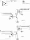
FIG. 1 illustrate the schematic symbol for the buffer circuit.
FIG. 1a illustrates the truth table for the buffer circuit.
FIG. 1b illustrates the buffer circuit using a single BJT transistor.
FIG. 1c illustrates the buffer circuit using a single FET transistor.
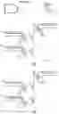
FIG. 2 illustrates the schematic symbol for the AND gate circuit.
FIG. 2a illustrates the truth table for the AND gate circuit.
FIG. 2b illustrates the AND gate circuit using two BJT's connected in series.
FIG. 2c illustrates the AND gate circuit using two FET's connected in series.
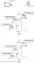
FIG. 3 illustrates the schematic symbol for the OR gate circuit.
FIG. 3a illustrates the truth table for the OR gate circuit.
FIG. 3b illustrates the OR gate circuit using two BJT's connected in parallel.
FIG. 3c illustrates the OR gate circuit using two FET's connected in parallel.
FIG. 4 illustrates the schematic symbol for the inverter or NOT gate circuit.
FIG. 4a illustrates the truth table for the inverter or NOT gate circuit.
FIG. 4b illustrates the inverter or NOT gate circuit using a single BJT.
FIG. 4c illustrates the inverter or NOT gate circuit using a single FET.
FIG. 5 illustrates the schematic symbol for the NAND gate circuit.
FIG. 5a illustrates the truth table for the NAND gate circuit.
FIG. 5b illustrates the NAND gate circuit using two BJT's connected in series.
FIG. 5c illustrates the NAND gate circuit using two FET's connected in series.
FIG. 6 illustrates the schematic symbol for the NOR gate circuit.
FIG. 6a illustrates the truth table for the NOR gate circuit.
FIG. 6b illustrates the NOR gate circuit using two BJT's connected in parallel.
FIG. 6c illustrates the NOR gate circuit using two FET's connected in parallel.
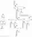
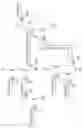
FIG. 7 illustrates a circuit design using the schematic symbols for the logic gate circuits.
FIG. 7a illustrates a detailed schematic of how the logic gates would connect to each other using BJT transistors.
FIG. 7b illustrates a detailed schematic of how the logic gates would connect to each other using FET transistors.
DETAILED DESCRIPTION
The schematic symbols in FIG. 1, FIG. 2, FIG. 3, FIG. 4, FIG. 5, FIG. 6, and FIG. 7 are like a short hand that is used to describe know functions of certain circuits. Instead of drawing the complete circuits the industry uses these symbols to describe a particular function on a schematic.
The truth tables in FIG. 1a, FIG. 2a, FIG. 3a, FIG. 4a, FIG. 5a, and FIG. 6a, are a mathematical description of the function of how each logic gate functions. The letters at the top of the truth table correspond to inputs and outputs on the circuits with the same labels. The numbers, 1's and 0's, are a universal representation of binary communication. The 1's are logical highs and in this case represent an input or output that is equal to the power source. The 0's are logical lows and in this case represent no input or output or 0 volts.
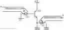
FIG. 1b is an illustration of a buffer circuit using a single BJT (Bipolar Junction Transistor), Q1. The photodiode, D1 is in it's photoconductive mode or reverse biased and is connected to the base of Q1. When light is applied to the fiber-optic line through input ‘A’, D1 will connect a positive voltage to the base of Q1 turning it on. Once Q1 is turned on it will connect a positive voltage to the anode of the LED, D2, forward biasing it. Once D2 is forward biased it will turn on and apply light though the fiber-optic lines through output ‘Y’. This would prove the truth table in FIG. 1a correct in that every logical high input will yield a logical high output. This design method is applicable to all types of BJT's.
FIG. 1c is an illustration of a buffer circuit using a single FET (Field Effect Transistor), Q1. The photodiode, D1 is in it's photoconductive mode or reverse biased and is connected to the gate of Q1. When light is applied to the fiber-optic line through input ‘A’, D1 will connect a positive voltage to the gate of Q1 turning it on. Once Q1 is turned on it will connect a positive voltage to the anode of the LED, D2, forward biasing it. Once D2 is forward biased it will turn on and apply light though the fiber-optic lines through output ‘Y’. This arrangement would prove the truth table in FIG. 1a correct in that every logical high input will yield a logical high output. This design method is applicable to all types of FET's.
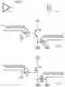
FIG. 2b is an illustration of an AND gate circuit using more than one BJT (Bipolar Junction Transistor), Q1 and Q2 connected in series from power to ground. The photodiode, D1, is in it's photoconductive mode or reverse biased and is connected to the base of Q1. The photodiode, D2 is in it's photoconductive mode or reverse biased and is connected to the base of Q2. When light is applied to the fiber-optic line through input ‘A’, D1 will connect a positive voltage to the base of Q1 turning it on. When light is applied to the fiber-optic line through input ‘B’, D2 will connect a positive voltage to the base of Q2 turning it on. Once both Q1 and Q2 is turned on they will connect a positive voltage to the anode of the LED, D3, forward biasing it. Once D2 is forward biased it will turn on and apply light though the fiber-optic lines through output ‘Y’. This arrangement would prove the truth table for an AND gate in FIG. 2a correct in that all logical high inputs will yield a logical high output. This design method includes all types of BJT's.
FIG. 2c is an illustration of an AND gate circuit using more than one FET (Field Effect Transistor), Q1 and Q2 connected in series from power to ground. The photodiode, D1, is in it's photoconductive mode or reverse biased and is connected to the gate of Q1. The photodiode, D2 is in it's photoconductive mode or reverse biased and is connected to the gate of Q2. When light is applied to the fiber-optic line through input ‘A’, D1 will connect a positive voltage to the gate of Q1 turning it on. When light is applied to the fiber-optic line through input ‘B’, D2 will connect a positive voltage to the gate of Q2 turning it on. Once both Q1 and Q2 is turned on they will connect a positive voltage to the anode of the LED, D3, forward biasing it. Once D2 is forward biased it will turn on and apply light though the fiber-optic lines through output ‘Y’. This arrangement would prove the truth table for an AND gate in FIG. 2a correct in that all logical high inputs will yield a logical high output. This design method includes all types of FET's.
FIG. 3b is an illustration of an OR gate circuit using more than one BJT (Bipolar Junction Transistor), case Q1 and Q2 connected in parallel from power to ground. The photodiode, D1, is in it's photoconductive mode or reverse biased and is connected to the base of Q1. The photodiode, D2 is in it's photoconductive mode or reverse biased and is connected to the base of Q2. When light is applied to the fiber-optic line through input ‘A’, D1 will connect a positive voltage to the base of Q1 turning it on. When light is applied to the fiber-optic line through input ‘B’, D2 will connect a positive voltage to the base of Q2 turning it on. Once either Q1 or Q2 is turned on they will connect a positive voltage to the anode of the LED, D3, forward biasing it. Once D2 is forward biased it will turn on and apply light though the fiber-optic lines through output ‘Y’. This arrangement would prove the truth table for an OR gate in FIG. 3a correct in that any logical high input will yield a logical high output. This design method includes all types of BJT's.
FIG. 3c is an illustration of an OR gate circuit using more than one FET (Field Effect Transistor), Q1 and Q2 connected in parallel from power to ground. The photodiode, D1, is in it's photoconductive mode or reverse biased and is connected to the gate of Q1. The photodiode, D2 is in it's photoconductive mode or reverse biased and is connected to the gate of Q2. When light is applied to the fiber-optic line through input ‘A’, D1 will connect a positive voltage to the gate of Q1 turning it on. When light is applied to the fiber-optic line through input ‘B’, D2 will connect a positive voltage to the gate of Q2 turning it on. Once either Q1 or Q2 is turned on they will connect a positive voltage to the anode of the LED, D3, forward biasing it. Once D2 is forward biased it will turn on and apply light though the fiber-optic lines labeled output ‘Y’. This arrangement would prove the truth table for an OR gate in FIG. 3a correct in that any logical high input will yield a logical high output. This design method includes all types of FET's.
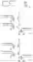
FIG. 4b is an illustration of a inverter or (NOT gate) circuit using a single BJT (Bipolar Junction Transistor), Q1. The photodiode, D1 is in it's photoconductive mode or reverse biased and is connected to the base of Q1. When light is applied to the fiber-optic line through input ‘A’, D1 will connect a positive voltage to the base of Q1 turning it on. Once Q1 is turned on it will shunt current away from the LED, D2, turning it off. Once D2 is off it will not apply light though the fiber-optic lines labeled output ‘Y’. This would prove the truth table in FIG. 4a correct in that every logical high input will yield a logical low output. This design method is applicable to all types of BJT's.
FIG. 4c is an illustration of an inverter or (NOT gate) circuit using a single FET (Field Effect Transistor), Q1. The photodiode, D1 is in it's photoconductive mode or reverse biased and is connected to the gate of Q1. When light is applied to the fiber-optic line through input ‘A’, D1 will connect a positive voltage to the gate of Q1 turning it on. Once Q1 is turned on it will shunt current away from the LED, D2, turning it off. Once D2 is off it will not apply light though the fiber-optic lines labeled output ‘Y’. This would prove the truth table in FIG. 4a correct in that every logical high input will yield a logical low output. This design method is applicable to all types of FET's.
FIG. 5b is an illustration of a NAND gate circuit using more than one BJT (Bipolar Junction Transistor), Q1 and Q2 connected in series from power to ground. The photodiode, D1, is in it's photoconductive mode or reverse biased and is connected to the base of Q1. The photodiode, D2 is in it's photoconductive mode or reverse biased and is connected to the base of Q2. When light is applied to the fiber-optic line through input ‘A’, D1 will connect a positive voltage to the base of Q1 turning it on. When light is applied to the fiber-optic line through input ‘B’, D2 will connect a positive voltage to the base of Q2 turning it on. Once both Q1 and Q2 is turned on they will shunt current away from the LED, D3, turning it off. If D3 is off it will not apply light though the fiber-optic lines labeled output ‘Y’. This arrangement would prove the truth table for an NAND gate in FIG. 5a correct in that all logical high inputs will yield a logical low output. This design method includes all types of BJT's.
FIG. 5c is an illustration of a NAND gate circuit using more than one FET (Field Effect Transistor), Q1 and Q2 connected in series from power to ground. The photodiode, D1, is in it's photoconductive mode or reverse biased and is connected to the gate of Q1. The photodiode, D2 is in it's photoconductive mode or reverse biased and is connected to the gate of Q2. When light is applied to the fiber-optic line through input ‘A’, D1 will connect a positive voltage to the gate of Q1 turning it on. When light is applied to the fiber-optic line through input ‘B’, D2 will connect a positive voltage to the gate of Q2 turning it on. Once both Q1 and Q2 is turned on they will shunt current away from the LED, D3, turning it off. If D3 is off it will not apply light though the fiber-optic lines labeled output ‘Y’. This arrangement would prove the truth table for an NAND gate in FIG. 5a correct in that all logical high inputs will yield a logical low output. This design method includes all types of FET's.
FIG. 6b is an illustration of an NOR gate circuit using more than one BJT (Bipolar Junction Transistor), Q1 and Q2 connected in parallel from power to ground. The photodiode, D1, is in it's photoconductive mode or reverse biased and is connected to the base of Q1. The photodiode, D2 is in it's photoconductive mode or reverse biased and is connected to the base of Q2. When light is applied to the fiber-optic line through input ‘A’, D1 will connect a positive voltage to the base of Q1 turning it on. When light is applied to the fiber-optic line through input ‘B’, D2 will connect a positive voltage to the base of Q2 turning it on. Once either Q1 or Q2 is turned on they will shunt current away from the LED, D3, turning it off. Once D3 is off it will not apply light though the fiber-optic lines labeled output ‘Y’. This arrangement would prove the truth table for an OR gate in FIG. 5a correct in that any logical high input will yield a logical low output. This design method includes all types of BJT's.
FIG. 6c is an illustration of an NOR gate circuit using more than one FET (Field Effect Transistor), Q1 and Q2 connected in parallel from power to ground. The photodiode, D1, is in it's photoconductive mode or reverse biased and is connected to the gate of Q1. The photodiode, D2 is in it's photoconductive mode or reverse biased and is connected to the gate of Q2. When light is applied to the fiber-optic line through input ‘A’, D1 will connect a positive voltage to the gate of Q1 turning it on. When light is applied to the fiber-optic line through input ‘B’, D2 will connect a positive voltage to the gate of Q2 turning it on. Once either Q1 or Q2 is turned on they will shunt current away from the LED, D3, turning it off. Once D3 is off it will not apply light though the fiber-optic lines labeled output ‘Y’. This arrangement would prove the truth table for an OR gate in FIG. 6a correct in that any logical high input will yield a logical low output. This design method includes all types of FET's.
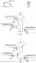
As seen in FIG. 7a illustrates how the logic gates themselves will connect to each other by fiber-optic transmission lines using BJT's. FIG. 7b illustrates how the logic gates themselves will connect to each other by fiber-optic transmission lines using FET's. enabling the design of faster, more efficient, and less error prone integrated circuits. Each of them have inputs labeled ‘A’, ‘B’, ‘C’, and ‘D’ and an output labeled ‘Y’. These illustrations are examples of connections between logic circuits and not actual logic gates themselves.
Claims
I claim:1. A logic family design method comprising:
a BJT having a base, emitter, and collector;
a photodiode having a cathode and an anode;
a FET having a gate source, and drain;
an LED having a cathode and an anode; and
A Fiber optic transmission line for connecting said logic circuits and transmitting binary information in the form of light between logic circuits.
2. The photodiode of claim 1 wherein said photodiode converts binary information in the form of light into equivalent electronic pulses of current to be processed by said transistor.
3. The LED of claim 1 wherein said LED converts binary information in the form of electronic pulses of current that have been processed by the transistor into light.
4. The fiber optic lines as in claim 1 wherein said fiber optic transmission lines are used as the transmission medium for binary information in the form of light connecting the LED of one logic circuit to the photodiode of the following logic circuit.
Images & Drawings included:
Sources:
- United States Patent and Trademark Office - verify current appl. status at the USPTO↗
Similar patent applications:
- » 20190285966
Fiber-optic connected logic (FOCL)
Recent applications in this class:
- » 20200358443 2020-11-12
Current steering level-shifter - » 20190013810 2019-01-10
System and method for complimentary VT-drop ambipolar carbon nanotube logic - » 16229617 2020-05-26
Current steering level-shifter