Circuits for modulated-mixer-clock multi-branch receivers
US20200099338A1
2020-03-26
16/579,782
2019-09-23
✅ Patent granted
US 10,819,284 B2
2020-10-27
-
-
Sonny Trinh
Byrne Poh LLP
2039-09-23
Abstract:
Circuits comprising: a plurality of LNTA branches, each comprising: a cascode common-source (CCS) LNTA, a plurality of passive mixers (PMs), and a plurality of baseband two-stage Miller compensated TIAs (BB2S-TIAs); a plurality of mixer-first branches, each comprising: a plurality of RF switches, a plurality of baseband folded-cascode TIAs (BBFC-TIAs), and a plurality of Cherry-Hooper amplifiers, wherein an input to each of the BBFC-TIAs is provided by an output of at least one of the RF switches, and an input to each of the amplifiers is provided by an output of a corresponding one of the BBFC-TIAs; a first plurality of clock modulators that provide first non-overlapping modulated clocks that are provided to an input of the PMs; and a second plurality of clock modulators that provide a plurality of tri-level modulated mixer clocks that control the switching of the RF switches.
Inventors:
- Peter R. Kinget 34 🇺🇸 Summit, NJ, United States
- Guoxiang Han 2 🇺🇸 New York, NY, United States
- Tanbir Haque 2 🇺🇸 New York, NY, United States
Assignee:
- The Trustees of Columbia University in the City of New York 2,382 🇺🇸 New York, NY, United States
Applicant:
Interested in similar patents?
Get notified when new applications in this technology area are published.
Classification:
H03F3/45179 » CPC further
Amplifiers with only discharge tubes or only semiconductor devices as amplifying elements; Differential amplifiers with semiconductor devices only characterised by the way of implementation of the active amplifying circuit in the differential amplifier using MOSFET transistors as the active amplifying circuit
H03F3/45403 » CPC further
Amplifiers with only discharge tubes or only semiconductor devices as amplifying elements; Differential amplifiers with semiconductor devices only characterised by the way of implementation of the active amplifying circuit in the differential amplifier using junction FET transistors as the active amplifying circuit; Pl types Folded cascode stages
H04B1/109 » CPC further
Details of transmission systems, not covered by a single one of groups - ; Details of transmission systems not characterised by the medium used for transmission; Receivers; Means associated with receiver for limiting or suppressing noise or interference by improving strong signal performance of the receiver when strong unwanted signals are present at the receiver input
H03D7/1466 » CPC main
Transference of modulation from one carrier to another, e.g. frequency-changing; Balanced arrangements with transistors Passive mixer arrangements
H03F1/0205 » CPC further
Details of amplifiers with only discharge tubes, only semiconductor devices or only unspecified devices as amplifying elements; Modifications of amplifiers to raise the efficiency, e.g. gliding Class A stages, use of an auxiliary oscillation in transistor amplifiers
H03F2200/294 » CPC further
Indexing scheme relating to amplifiers the amplifier being a low noise amplifier [LNA]
H03F2203/45024 » CPC further
Indexing scheme relating to amplifiers with only discharge tubes or only semiconductor devices as amplifying elements covered by; Indexing scheme relating to differential amplifiers the differential amplifier amplifying transistors are cascode coupled transistors
H04B1/10 IPC
Details of transmission systems, not covered by a single one of groups - ; Details of transmission systems not characterised by the medium used for transmission; Receivers Means associated with receiver for limiting or suppressing noise or interference
H03D7/14 IPC
Transference of modulation from one carrier to another, e.g. frequency-changing Balanced arrangements
H03F3/193 » CPC further
Amplifiers with only discharge tubes or only semiconductor devices as amplifying elements; High frequency amplifiers, e.g. radio frequency amplifiers with semiconductor devices only with field-effect devices
H03F3/45 IPC
Amplifiers with only discharge tubes or only semiconductor devices as amplifying elements Differential amplifiers
H03F1/26 » CPC further
Details of amplifiers with only discharge tubes, only semiconductor devices or only unspecified devices as amplifying elements Modifications of amplifiers to reduce influence of noise generated by amplifying elements
H04B1/16 » CPC further
Details of transmission systems, not covered by a single one of groups - ; Details of transmission systems not characterised by the medium used for transmission; Receivers Circuits
H03F1/02 IPC
Details of amplifiers with only discharge tubes, only semiconductor devices or only unspecified devices as amplifying elements Modifications of amplifiers to raise the efficiency, e.g. gliding Class A stages, use of an auxiliary oscillation
Description
CROSS REFERENCE TO RELATED APPLICATION
This application claims the benefit of U.S. Provisional Patent Application No. 62/734,957, filed Sep. 21, 2018, which is hereby incorporated by reference herein in its entirety.
STATEMENT REGARDING FEDERALLY SPONSORED RESEARCH OR DEVELOPMENT
This invention was made with government support under grant 1733857 awarded by the National Science Foundation. The government has certain rights in the invention.
BACKGROUND
Current circuits for receiving multiple frequencies at the same time suffer from many performance problems.
Accordingly, it is desirable to provide new circuits for receiving multiple frequencies at the same time.
SUMMARY
Circuits for modulated-mixer-clock multi-branch receivers are provided. In some embodiments, circuits for modulated-mixer-clock multi-branch receivers comprise: a plurality of low-noise transconductance amplifier (LNTA) branches, each comprising: a cascode common-source LNTA, a plurality of passive mixers, and a plurality of baseband two-stage Miller compensated transimpedance amplifiers (TIAs), wherein an input to the cascode common-source LNTA is provided by a radio frequency (RF) signal source, an input to each of the plurality of passive mixers is provided by an output of the cascode common-source LNTA, and an input to each of the plurality of baseband two-stage Miller compensated TIAs is provided by an output of a corresponding one of the plurality of passive mixers; a plurality of mixer-first branches, each comprising: a plurality of RF switches, a plurality of baseband folded-cascode TIAs, and a plurality of Cherry-Hooper amplifiers, wherein an input to the plurality of RF switches is provided by the RF signal source, an input to each of the plurality of baseband folded-cascode TIAs is provided by an output of at least one of the plurality of RF switches, and an input to each of the plurality of Cherry-Hooper amplifiers is provided by an output of a corresponding one of the plurality of baseband folded-cascode TIAs; a first plurality of clock modulators that provide first non-overlapping modulated clocks that are provided to an input of the plurality of passive mixers; and a second plurality of clock modulators that provide a plurality of tri-level modulated mixer clocks that control the switching of the plurality of RF switches.
BRIEF DESCRIPTION OF THE DRAWINGS
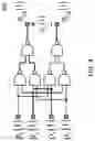
FIG. 1 is an example of a receiver in accordance with some embodiments.
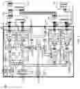
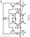
FIG. 2 is an example of a clock modulator, four mixer-first branches (illustrated in single-ended form), and a band separation circuit that can be used in a receiver in accordance with some embodiments.
FIG. 3 is an example of a cascode common-source low noise transconductance amplifier that can be used in a receiver in accordance with some embodiments.
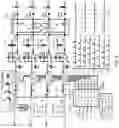
FIG. 4 is an example of a clock modulator cell that can be used in a receiver in accordance with some embodiments.
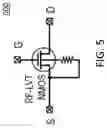
FIG. 5 is an example of an RF switch that can be used in a receiver in accordance with some embodiments.
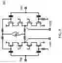
FIG. 6 is an example of a Cherry-Hooper amplifier that can be used in a receiver in accordance with some embodiments.
DETAILED DESCRIPTION
In accordance with some embodiments, modulated-mixer-clock (MMC) multi-branch receivers are provided.
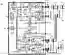
In some embodiments, a modulated-mixer-clock (MMC) multi-branch receiver can be implemented as shown by example receiver 100 of FIG. 1. As illustrated, receiver 100 can include a two low-noise transconductance amplifier (LNTA) branches (LB1 102 and LB2 104), two mixer-first branches (MFB1 106 and MFB2 108), clock path circuitry 110, band separation circuits 112 and 114, noise cancellation circuits 116, and compressive sampling digital signal processor (DSP) 118 in some embodiments.
Each of LNTA branches LB1 102 and LB2 104 in receiver 100 can include a cascode common-source LNTA (Gm) 120, differential passive mixers 122, and baseband two-stage Miller compensated trans-impedance amplifiers (TIAs) 124 in some embodiments.
An example 300 of a circuit that can be used to implement cascode common-source LNTA (Gm) 120 in accordance with some embodiments is shown in FIG. 3.
Each of mixer-first branches MFB1 106 and MFB2 108 can include RF switches 126, baseband folded-cascode TIAs 128, and Cherry-Hooper amplifiers with programmable degeneration and feedback resistors for gain and linearity control 130 in some embodiments.
RF switches 126 can be placed in a floating-body configuration to decrease their OFF capacitance and biased at a 0.2V source terminal voltage to reduce their ON resistance in some embodiments. An example 500 of a floating-body radio-frequency low-voltage threshold (RF-LVT) NMOS switch that can be used to implement an RF switch 126 in accordance with some embodiments is shown in FIG. 5.
An example 600 of a Cherry-Hooper amplifier that can be used to implement amplifier 130 in accordance with some embodiments is shown in FIG. 6.
Clock path circuitry can include clock dividers, non-overlapping clock generators, two clock modulators, and a pseudo-random bit sequence (PRBS) synthesizer in some embodiments.
In some embodiments, the clock modulators can be implemented with NAND-based logic with delay-matching for all clock inputs. An example 400 of a clock modulator cell for phase ϕ0 that can be used to implement a clock modulator (shown in FIG. 1) in accordance with some embodiments is shown in FIG. 4. Similar clock modulator cells can be implemented for ϕ1, ϕ2, and ϕ3 by modifying clock modulator cell 400 consistent with the equations in box 202 of FIG. 2 in some embodiments.
The PRBS synthesizer can be any suitable PRBS synthesizer in some embodiments. In some embodiments, the PRBS synthesizer can generate both shift-register-based and linear feedback shift register (LFSR)-based PRBS sequences of any suitable length. In some embodiments, the PRBS synthesizer can be a Gold sequence generator.
In some embodiments, the LNTA branches and the mixer-first branches can operate independently with different clock sources or can be driven synchronously with the same clock. For example, in some embodiments, receiver 100 can operate in any one or more of a single-carrier reception mode, a dual-carrier reception mode, and compressive sampling scanning mode. In the single-carrier reception mode in some embodiments, only the LB1 branch and the MBF1 branch are turned on. In the dual-carrier reception mode in some embodiments, both LNTA branches and both mixer-first branches are active. In the compressive sampling scanning mode in some embodiments, the two LNTA branches are powered off and both mixer-first branches are active.
During operation, receiver 100 can use mixer-clock modulation to achieve dual-band tuned matching and concurrent dual carrier reception in some embodiments. In some embodiments, to receive signals at FRF1 and FRF2, a 4-phase non-overlapping RF clock at FC=(FRF1+FRF2)/2 can be modulated with a modulation clock at FM=(FRF1−FRF1)/2. When applying these modulated clocks to the mixer-first branches, the baseband impedance can be translated as a tuned response at FRF1 and FRF2 in some embodiments. Alternatively, if pseudo-random bit sequences (PRBS) are modulated on the RF clock (FC), the mixer-first branches can perform compressive-sampling (CS) wideband spectrum scanning.
As shown in FIG. 2, in some embodiments, four tri-level-modulated mixer clocks ϕ0-ϕ3 can be derived from two 4-phase 25% non-overlapping clocks p0-3(t) and ρ0-3(t) at FC and FM, respectively, using a digital clock modulator 202 by either flipping or not flipping the polarity of the input clocks, or holding the outputs low as described by the formulas in box 202. When flipping the RF clock at a rate FM in FIG. 2, the FC tone in the RF clock is moved to two tones at FRF1=FC−FM and FRF2=FC+FM. When one modulated clock of ϕ0-ϕ3 is low in FIG. 2, the other three modulated clocks of ϕ0-ϕ3 are switching. The four clocks ϕ0-ϕ3 can be guaranteed to be non-overlapping and have linearly-independent spectra in some embodiments.
Applying ϕ0-ϕ3 to mixer-first branches 204, 206, 208, and 210 (which are shown in a single ended configuration for purposes of clarity) translates the baseband impedance to FRF1 and FRF2 and achieves dual-band impedance matching. Meanwhile, the mixer-first branches concurrently down-convert the RF input signals at FRF1 and FRF2 to linearly independent baseband outputs. Simple addition and subtraction in band separation circuit 212 can be used to separate the I/Q components for each RF band to produce outputs LB-Q, LB-I, HB-I, and HB-Q.
A benefit of clock modulation in some embodiments is that the clock sources FC and FM are separated more widely than FRF1 and FRF2, which alleviates possible phase-locked loop (PLL) pulling issues. While spurious tones can exist in the modulated clocks due to intermixing of higher order harmonics of FC or FM in some embodiments, those spurious tones are expected to be out of band or mitigatable with frequency planning in some embodiments.
In some embodiments, low noise transconductance amplifiers (LNTA) branches, LB1 and LB2, driven by modulated clock sets CLKLB1 and CLKLB2 can be used to implement noise cancellation and improves the noise figure (NF) of the receiver. The two pairs of non-overlapping modulated clock sets CLKLB1 and CLKLB2 can be generated with 50% 4-phase FM clocks to modulate the 25% 4-phase FC RF clock.
In some embodiments, during a compressive sampling (CS) mode, clock FC can be 700 MHz and be modulated with a maximal-length PRBS sequence of length L=63 clocked at FM equal to 630 MHz. In some embodiments, during CS wideband scanning (e.g., with a CW input tone at 662 MHz, and two noise-modulated 2 MHz wide input signals at 693 MHz and 729 MHz), the mixer first branches with pseudo-random modulated clocks can down-convert the RF signals to baseband. The resulting signals can then be processed by CS DSP 118 (FIG. 1) which can use any suitable CS processing techniques as known in the art to identify signals in the scanned region.
Although specific components are described herein, it should be apparent that other components can be used to provide the same or similar functions and/or additional functions in some embodiments.
Although the invention has been described and illustrated in the foregoing illustrative embodiments, it is understood that the present disclosure has been made only by way of example, and that numerous changes in the details of implementation of the invention can be made without departing from the spirit and scope of the invention, which is limited only by the claims that follow. Features of the disclosed embodiments can be combined and rearranged in various ways
Claims
What is claimed is:1. A circuit for a modulated-mixer-clock multi-branch receiver, comprising:
a plurality of low-noise transconductance amplifier (LNTA) branches, each comprising:
a cascode common-source LNTA,
a plurality of passive mixers, and
a plurality of baseband two-stage Miller compensated transimpedance amplifiers (TIAs),
wherein an input to the cascode common-source LNTA is provided by a radio frequency (RF) signal source, an input to each of the plurality of passive mixers is provided by an output of the cascode common-source LNTA, and an input to each of the plurality of baseband two-stage Miller compensated TIAs is provided by an output of a corresponding one of the plurality of passive mixers;
a plurality of mixer-first branches, each comprising:
a plurality of RF switches,
a plurality of baseband folded-cascode TIAs, and
a plurality of Cherry-Hooper amplifiers,
wherein an input to the plurality of RF switches is provided by the RF signal source, an input to each of the plurality of baseband folded-cascode TIAs is provided by an output of at least one of the plurality of RF switches, and an input to each of the plurality of Cherry-Hooper amplifiers is provided by an output of a corresponding one of the plurality of baseband folded-cascode TIAs;
a first plurality of clock modulators that provide first non-overlapping modulated clocks that are provided to an input of the plurality of passive mixers; and
a second plurality of clock modulators that provide a plurality of tri-level modulated mixer clocks that control the switching of the plurality of RF switches.
Images & Drawings included:
Sources:
- United States Patent and Trademark Office - verify current appl. status at the USPTO↗
Recent applications in this class:
- » 20240421769 2024-12-19
Methods and Circuitry for Reducing Mixer Harmonics Conversion Gain and Local Oscillator Fundamental and Harmonics Feedthrough - » 20230396216 2023-12-07
Receiver Circuit - » 20230043914 2023-02-09
Up/down frequency converter with millimeter-wave low-phase-noise local oscillator - » 20220321058 2022-10-06
Mixer circuitry with noise cancellation - » 20220094304 2022-03-24
Mixer circuitry with noise cancellation - » 20190190452 2019-06-20
Passive mixer - » 20180278211 2018-09-27
Radio receiver for carrier aggregation - » 20180041168 2018-02-08
System and method for linearizing a transmitter by rejecting harmonics at mixer output - » 20160241193 2016-08-18
Radio receiver for carrier aggregation - » 20150381112 2015-12-31
FILTER WITH AN AUXILIARY MIXING PATH
Recent applications for this Assignee:
- » 20250290113 2025-09-18
MODIFIED BACTERIAL PROTEIN EXPRESSION SYSTEM - » 20250284135 2025-09-11
Four-Way Image Splitter for High-Speed Characterization of Tissue Samples - » 20250278625 2025-09-04
VISUOMOTOR POLICY LEARNING VIA ACTION DIFFUSION - » 20250277800 2025-09-04
NUCLEIC ACID SEQUENCES RESPONSIVE TO CREATININE IN CLINICALLY USEFUL RANGES - » 20250273228 2025-08-28
Systems and Methods for Enhancing Auditory Attention Decoding Using Spatial Cues - » 20250270385 2025-08-28
DYNAMICALLY CROSSLINKED MULTIBLOCK COPOLYMERS FOR COMPATIBILIZING IMMISCIBLE MIXED PLASTICS - » 20250264398 2025-08-21
Systems and Methods for Identifying and Recovering Rare Biological Cells from a Sample - » 20250255976 2025-08-14
CATIONIC BIOMATERIALS AMELIORATE OBESITY-ASSOCIATED CHRONIC INFLAMMATION AND FOCAL ADIPOSITY - » 20250252263 2025-08-07
Systems and Methods for Detecting Generated Text Through Rewriting Operations - » 20250243537 2025-07-31
SYNTHESIS OF CLEAVABLE FLUORESCENT NUCLEOTIDES AS REVERSIBLE TERMINATORS FOR DNA SEQUENCING BY SYNTHESIS