Method of forming memory cell
US20210343789A1
2021-11-04
17/375,021
2021-07-14
✅ Patent granted
US 11,632,889 B2
2023-04-18
-
-
Dao H Nguyen
Winston Hsu
2041-08-13
Abstract:
A memory cell includes a first conductive line, a lower electrode, a carbon nano-tube (CNT) layer, a middle electrode, a resistive layer, a top electrode and a second conductive line. The first conductive line is disposed over a substrate. The lower electrode is disposed over the first conductive line. The carbon nano-tube (CNT) layer is disposed over the lower electrode. The middle electrode is disposed over the carbon nano-tube layer, thereby the lower electrode, the carbon nano-tube (CNT) layer and the middle electrode constituting a nanotube memory part. The resistive layer is disposed over the middle electrode. The top electrode is disposed over the resistive layer, thereby the middle electrode, the resistive layer and the top electrode constituting a resistive memory part. The second conductive line is disposed over the top electrode.
Inventors:
- Ya-Jyuan Hung 11 🇹🇼 Kaohsiung City, Taiwan
- Bin-Siang Tsai 118 🇹🇼 Changhua County, Taiwan
- Da-Jun Lin 79 🇹🇼 Kaohsiung City, Taiwan
- Chin-Chia Yang 9 🇹🇼 Tainan City, Taiwan
- Ting-An Chien 27 🇹🇼 Tainan City, Taiwan
- Da-Jun Lin 46 🇹🇼 Kaohsiung, Taiwan
- Ting-An Chien 23 🇹🇼 Tainan, Taiwan
- Chin-Chia Yang 6 🇹🇼 Tainan, Taiwan
- Ya-Jyuan Hung 7 🇹🇼 Kaohsiung, Taiwan
Assignee:
- UNITED MICROELECTRONICS CORP. 1,139 🇹🇼 Hsin-Chu City, Taiwan
- UNITED MICROELECTRONICS CORP. 2,360 🇹🇼 Hsin-Chu, Taiwan
Applicant:
Interested in similar patents?
Get notified when new applications in this technology area are published.
Classification:
H01L27/2481 » CPC main
Devices consisting of a plurality of semiconductor or other solid-state components formed in or on a common substrate including solid state components for rectifying, amplifying or switching without a potential-jump barrier or surface barrier, e.g. resistance switching non-volatile memory structures; Arrangements comprising multiple bistable or multistable switching components of the same type on a plane parallel to the substrate, e.g. cross-point arrays, details of the horizontal layout arranged in a direction perpendicular to the substrate, e.g. 3D cell arrays, details of the vertical layout
H01L27/285 » CPC further
Devices consisting of a plurality of semiconductor or other solid-state components formed in or on a common substrate including components using organic materials as the active part, or using a combination of organic materials with other materials as the active part Integrated circuits with a common active layer, e.g. cross point devices
H01L45/08 » CPC further
Solid state devices adapted for rectifying, amplifying, oscillating or switching without a potential-jump barrier or surface barrier, e.g. dielectric triodes; Ovshinsky-effect devices; Processes or apparatus peculiar to the manufacture or treatment thereof or of parts thereof; Bistable or multistable switching devices, e.g. for resistance switching non-volatile memory based on migration or redistribution of ionic species, e.g. anions, vacancies
H01L45/1233 » CPC further
Solid state devices adapted for rectifying, amplifying, oscillating or switching without a potential-jump barrier or surface barrier, e.g. dielectric triodes; Ovshinsky-effect devices; Processes or apparatus peculiar to the manufacture or treatment thereof or of parts thereof; Bistable or multistable switching devices, e.g. for resistance switching non-volatile memory; Details; Device geometry adapted for essentially vertical current flow, e.g. sandwich or pillar type devices
H01L45/1253 » CPC further
Solid state devices adapted for rectifying, amplifying, oscillating or switching without a potential-jump barrier or surface barrier, e.g. dielectric triodes; Ovshinsky-effect devices; Processes or apparatus peculiar to the manufacture or treatment thereof or of parts thereof; Bistable or multistable switching devices, e.g. for resistance switching non-volatile memory; Details Electrodes
H01L51/102 » CPC further
Solid state devices using organic materials as the active part, or using a combination of organic materials with other materials as the active part; Processes or apparatus specially adapted for the manufacture or treatment of such devices, or of parts thereof specially adapted for rectifying, amplifying, oscillating or switching, or capacitors or resistors with at least one potential- jump barrier or surface barrier multistep processes for their manufacture; Details of devices Electrodes
H01L45/1675 » CPC further
Solid state devices adapted for rectifying, amplifying, oscillating or switching without a potential-jump barrier or surface barrier, e.g. dielectric triodes; Ovshinsky-effect devices; Processes or apparatus peculiar to the manufacture or treatment thereof or of parts thereof; Bistable or multistable switching devices, e.g. for resistance switching non-volatile memory; Manufacturing; Patterning of the switching material by etching of pre-deposited switching material layers, e.g. lithography
H01L51/0017 » CPC further
Solid state devices using organic materials as the active part, or using a combination of organic materials with other materials as the active part; Processes or apparatus specially adapted for the manufacture or treatment of such devices, or of parts thereof; Processes specially adapted for the manufacture or treatment of devices or of parts thereof for changing the shape of the device layer, e.g. patterning etching of an existing layer
H01L51/0048 » CPC further
Solid state devices using organic materials as the active part, or using a combination of organic materials with other materials as the active part; Processes or apparatus specially adapted for the manufacture or treatment of such devices, or of parts thereof; Selection of organic semiconducting materials, e.g. organic light sensitive or organic light emitting materials; Carbon containing materials, e.g. carbon nanotubes, fullerenes Carbon nanotubes
H01L51/0591 » CPC further
Solid state devices using organic materials as the active part, or using a combination of organic materials with other materials as the active part; Processes or apparatus specially adapted for the manufacture or treatment of such devices, or of parts thereof specially adapted for rectifying, amplifying, oscillating or switching, or capacitors or resistors with at least one potential- jump barrier or surface barrier multistep processes for their manufacture the devices being controllable only by variation of the electric current supplied or the electric potential applied, to one or more of the electrodes carrying the current to be rectified, amplified, oscillated or switched, e.g. two-terminal devices Bi-stable switching devices
H01L45/146 » CPC further
Solid state devices adapted for rectifying, amplifying, oscillating or switching without a potential-jump barrier or surface barrier, e.g. dielectric triodes; Ovshinsky-effect devices; Processes or apparatus peculiar to the manufacture or treatment thereof or of parts thereof; Bistable or multistable switching devices, e.g. for resistance switching non-volatile memory; Selection of switching materials; Oxides or nitrides Binary metal oxides, e.g. TaOx
H01L27/24 IPC
Devices consisting of a plurality of semiconductor or other solid-state components formed in or on a common substrate including solid state components for rectifying, amplifying or switching without a potential-jump barrier or surface barrier, e.g. resistance switching non-volatile memory structures
H01L27/28 IPC
Devices consisting of a plurality of semiconductor or other solid-state components formed in or on a common substrate including components using organic materials as the active part, or using a combination of organic materials with other materials as the active part
H01L45/00 IPC
Solid state devices adapted for rectifying, amplifying, oscillating or switching without a potential-jump barrier or surface barrier, e.g. dielectric triodes; Ovshinsky-effect devices; Processes or apparatus peculiar to the manufacture or treatment thereof or of parts thereof
H01L51/00 IPC
Solid state devices using organic materials as the active part, or using a combination of organic materials with other materials as the active part; Processes or apparatus specially adapted for the manufacture or treatment of such devices, or of parts thereof
H01L51/05 IPC
Solid state devices using organic materials as the active part, or using a combination of organic materials with other materials as the active part; Processes or apparatus specially adapted for the manufacture or treatment of such devices, or of parts thereof specially adapted for rectifying, amplifying, oscillating or switching, or capacitors or resistors with at least one potential- jump barrier or surface barrier multistep processes for their manufacture
H01L51/10 IPC
Solid state devices using organic materials as the active part, or using a combination of organic materials with other materials as the active part; Processes or apparatus specially adapted for the manufacture or treatment of such devices, or of parts thereof specially adapted for rectifying, amplifying, oscillating or switching, or capacitors or resistors with at least one potential- jump barrier or surface barrier multistep processes for their manufacture Details of devices
Description
CROSS REFERENCE TO RELATED APPLICATIONS
This application is a divisional application of and claims the benefit of U.S. patent application Ser. No. 16/513,719, filed Jul. 17, 2019.
BACKGROUND OF THE INVENTION
1. Field of the Invention
The present invention relates generally to a memory cell and forming method thereof, and more specifically to a memory cell integrating a nanotube memory cell and a resistive memory cell and forming method thereof.
2. Description of the Prior Art
Digital logic circuits are used in control circuits of personal computers, electronic entertainment devices, telephone exchange systems, automobiles, aircraft, and other manufacturing items. Digital logic circuits can include individual or integrated logic functions and memory functions on wafers, and it is necessary to continuously increase the integration of logic functions and memory functions as the electronic devices develop.
Memory is divided into two categories: volatile memory and non-volatile memory. In nowadays, the two important types of volatile memory are static random access memory (SRAM) and dynamic random access memory (DRAM). There are many types of non-volatile memory. Flash memory is the most popular type, and other types may include silicon-oxide-nitride-oxide-silicon (SONOS), ferroelectric random access memory (FRAM), phase-change random access memory (PRAM), magnetoresistive access memory (MRAM) and resistive random access memory (RRAM).
Nanotube random access memory (NRAM) is also presented. Carbon nanotubes are distributed on a sheet substrate, and the carbon nanotubes attract or repel each other while signal writing. Each physical state (attracting or repelling) corresponds to a circuit state. The repulsion state is an open circuit state, while the attraction state is a closed state in which a rectifying junction is formed. When power is removed from the junction, its physical state is maintained, thereby forming a non-volatile memory unit.
SUMMARY OF THE INVENTION
The present invention provides a memory cell and forming method thereof, which integrates a nanotube memory cell with a resistive memory cell, thereby doubling the memory density of one memory cell.
The present invention provides a memory cell including a first conductive line, a lower electrode, a carbon nano-tube (CNT) layer, a middle electrode, a resistive layer, a top electrode and a second conductive line. The first conductive line is disposed over a substrate. The lower electrode is disposed over the first conductive line. The carbon nano-tube (CNT) layer is disposed over the lower electrode. The middle electrode is disposed over the carbon nano-tube layer, thereby the lower electrode, the carbon nano-tube (CNT) layer and the middle electrode constituting a nanotube memory part. The resistive layer is disposed over the middle electrode. The top electrode is disposed over the resistive layer, thereby the middle electrode, the resistive layer and the top electrode constituting a resistive memory part. The second conductive line is disposed over the top electrode.
The present invention provides a method of forming memory cell including the following steps. A first conductive line is formed over a substrate. A lower electrode layer, a blanket carbon nano-tube (CNT) layer, a middle electrode layer, a blanket resistive layer and a top electrode layer are formed on the first conductive line sequentially. The top electrode layer, the blanket resistive layer, the middle electrode layer, the blanket carbon nano-tube (CNT) layer and the lower electrode layer are patterned to forma lower electrode, a carbon nano-tube (CNT) layer, a middle electrode, a resistive layer and a top electrode stacked from bottom to top, thereby the lower electrode, the carbon nano-tube (CNT) layer and the middle electrode constituting a nanotube memory part, and the middle electrode, the resistive layer and the top electrode constituting a resistive memory part.
According to the above, the present invention provides a memory cell and forming method thereof, which forms a first conductive line on a substrate; a lower electrode on the first conductive line; a carbon nano-tube (CNT) layer on the lower electrode; a middle electrode on the carbon nano-tube (CNT) layer; a resistive layer on the middle electrode; a top electrode on the resistive layer; and, a second conductive line on the top electrode. Thereby, the lower electrode, the carbon nano-tube (CNT) layer and the middle electrode constitute a nanotube memory part, and the middle electrode, the resistive layer and the top electrode constitute a resistive memory part. This integrates a nanotube memory cell with a resistive memory cell, and thus forms a twin-bit memory cell, and doubles the memory density of one memory cell.
These and other objectives of the present invention will no doubt become obvious to those of ordinary skill in the art after reading the following detailed description of the preferred embodiment that is illustrated in the various figures and drawings.
BRIEF DESCRIPTION OF THE DRAWINGS
FIG. 1 schematically depicts a cross-sectional view of a method of forming memory cell according to an embodiment of the present invention.
FIG. 2 schematically depicts a cross-sectional view of a method of forming memory cell according to an embodiment of the present invention.
FIG. 3 schematically depicts a cross-sectional view of a method of forming memory cell according to an embodiment of the present invention.
FIG. 4 schematically depicts a cross-sectional view of a method of forming memory cell according to an embodiment of the present invention.
FIG. 5 schematically depicts a cross-sectional view of a method of forming memory cell according to an embodiment of the present invention.
FIG. 6 schematically depicts a cross-sectional view of a method of forming memory cell according to an embodiment of the present invention.
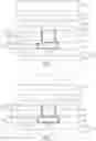
DETAILED DESCRIPTION
FIGS. 1-6 schematically depict cross-sectional views of a method of forming memory cell according to an embodiment of the present invention. As shown in FIG. 1, a substrate 110 is provided. The substrate 110 may include a bottom substrate 112, a transistor M, a contact plug C and an interlayer dielectric layer 114, wherein the transistor M is on the bottom substrate 112, and the transistor M and the contact plug C electrically connected to the transistor M are formed in the interlayer dielectric layer 114 on the bottom substrate 112, but it is not limited thereto. The bottom substrate 112 may be a semiconductor substrate such as a silicon substrate, a silicon containing substrate, a III-V group-on-silicon (such as GaN-on-silicon) substrate, a graphene-on-silicon substrate, a silicon-on-insulator (SOI) substrate or a substrate containing epitaxial layers; the transistor M may be a transistor having a polysilicon gate or a transistor having a metal gate etc; the interlayer dielectric layer 114 may be an oxide layer; the contact plug C may be composed of copper, tungsten or etc, and the contact plug C may formed by forming a recess in the interlayer dielectric layer 114 and then filling the contact plug C into the recess, but it is not limited thereto.
A conductive line 122 is formed on the substrate 110. The conductive line 122 may include a barrier layer 122a and a metal 122b, wherein the barrier layer 122a surrounds the metal 122b. The barrier layer 122a may be constituted by titanium nitride or/and tantalum nitride, and the metal 122b may be constituted by copper or tungsten, but it is not limited thereto. More precisely, a dielectric layer (not shown) may be formed and then patterned (or etched) to form a dielectric layer 124 on the substrate 110, wherein the dielectric layer 124 has a recess R1, and the conductive line 122 is formed in the recess R1. The dielectric layer 124 may be a dielectric layer with an ultra-low dielectric constant, but it is not restricted thereto.
A first conductive line 132 is formed on the conductive line 122. In this embodiment, the first conductive line 132 includes a metal line, and the first conductive line 132 may include a barrier layer 132a and a metal 132b, wherein the barrier layer 132a surrounds the metal 132b, but it is not limited thereto. The barrier layer 132a may be constituted by titanium nitride or/and tantalum nitride, and the metal 132b may be constituted by copper or tungsten, but it is not limited thereto. More precisely, a selective cap layer (not shown) and a first dielectric layer (not shown) may be sequentially formed on the conductive line 122 and the dielectric layer 124, therefore a cap layer 10 and a first dielectric layer 134 being formed on the conductive line 122 and the dielectric layer 124, wherein the cap layer 10 and the first dielectric layer 134 have a recess R2, and then the first conductive line 132 is formed in the recess R2. A barrier layer (not shown) and a metal (not shown) may sequentially fill into the recess R2 to form the first conductive line 132 in the recess R2. The cap layer 10 may be a nitrogen doped carbon silicon layer, and the first dielectric layer 134 may be a plasma enhanced oxide (PEOX) layer, but it is not restricted thereto.
A lower electrode layer 142′, a blanket carbon nano-tube (CNT) layer 144′, a middle electrode layer 146′, a blanket resistive layer 148′ and a top electrode layer 149′ may be sequentially formed on the first conductive line 132 and the first dielectric layer 134 from bottom to top. In this embodiment, the lower electrode layer 142′, the middle electrode layer 146′ and the top electrode layer 149′ may be titanium nitride layers; the blanket carbon nano-tube (CNT) layer 144′ may be stacked material layers, and these material layers have different conductive properties; the blanket resistive layer 148′ may be a stacked resistive layer, but it is not limited thereto. Preferably, the blanket resistive layer 148′ may include a tantalum oxide (TaOx) layer and a tantalum oxide (Ta2O5) layer stacked from bottom to top, wherein the tantalum oxide (TaOx) layer serves as a buffer layer. Then, a mask layer 150′ may cover the top electrode layer 149′ blanketly, wherein the mask layer 150′ may be a nitride layer, but it is not limited thereto.
Please refer to FIGS. 2-3, the top electrode layer 149′, the blanket resistive layer 148′, the middle electrode layer 146′, the blanket carbon nano-tube (CNT) layer 144′ and the lower electrode layer 142′ may be patterned to form a lower electrode 142, a carbon nano-tube (CNT) layer 144, a middle electrode 146, a resistive layer 148 and a top electrode 149 stacked from bottom to top, thereby the lower electrode 142, the carbon nano-tube (CNT) layer 144 and the middle electrode 146 constituting a nanotube memory part K1, and the middle electrode 146, the resistive layer 148 and the top electrode 149 constituting a resistive memory part K2.
More precisely, as shown in FIG. 2, the mask layer 150′ is patterned to form a mask layer 150 on the top electrode layer 149′ and expose an area would be removed. As shown in FIG. 3, the top electrode layer 149′, the blanket resistive layer 148′, the middle electrode layer 146′, the blanket carbon nano-tube (CNT) layer 144′ and the lower electrode layer 142′ may be patterned to form the lower electrode 142, the carbon nano-tube (CNT) layer 144, the middle electrode 146, the resistive layer 148 and the top electrode 149 stacked from bottom to top. The lower electrode 142 directly contacts and is electrically connected to the first conductive line 132. These stacked material layers constitute the nanotube memory part K1 and the resistive memory part K2, and the nanotube memory part K1 and the resistive memory part K2 share the middle electrode 146, thereby a twin-bit memory cell being formed by adjusting different voltage sections, wherein the twin-bit memory cell is a bipolar component. As a positive voltage of 2 volts is applied, the nanotube memory part K1 and the resistive memory part K2 turn on, called (1, 1) state. As a positive voltage of 1 volt is applied, only the nanotube memory part K1 turns on, called (0, 1) state. As a negative voltage of 1 volt is applied, only the resistive memory part K2 turns on, called (1, 0) state. As a negative voltage of 3 volts is applied, the nanotube memory part K1 and the resistive memory part K2 turn off, called (0, 0) state. Thus, the memory cell of the present invention has double memory density, smaller volume and low processing costs.
As shown in FIG. 4, a cap layer 160 conformally covers a top surface of the first dielectric layer 134, a top surface of the top electrode 149, and sidewalls of the lower electrode 142, the carbon nano-tube (CNT) layer 144, the middle electrode 146, the resistive layer 148 and the top electrode 149. The cap layer 160 may be a nitride layer or a carbon containing nitride layer, but it is not limited thereto.
As shown in FIG. 5, a second dielectric layer 170 is deposited to cover the first dielectric layer 134, the lower electrode 142, the carbon nano-tube (CNT) layer 144, the middle electrode 146, the resistive layer 148 and the top electrode 149 blanketly. A mask layer 180 may be selectively formed on the second dielectric layer 170. The mask layer 180 may be a SaC and CAPOx layer, but it is not restricted thereto.
After the second dielectric layer 170 or the mask layer 180 is formed, the second dielectric layer 170 and the mask layer 180 are etched to form a recess R3 in a cap layer 160a and a second dielectric layer 170a and expose the top electrode 149, as shown in FIG. 6. A second conductive line 192 is formed in the recess R3 and directly on the top electrode 149. Thereafter, the second conductive line 192 and the mask layer 180 exceeding from the recess R3 are removed. In this case, the second conductive line 192 may include a metal line, and the second conductive line 192 may include a barrier layer 192a and a metal 192b, wherein the barrier layer 192a surrounds the metal 192b, but it is not limited thereto. The barrier layer 192a may be constituted by titanium nitride or/and tantalum nitride, and the metal 192b may be constituted by copper or tungsten, but it is not limited thereto.
To summarize, the present invention provides a memory cell and forming method thereof, which forms a first conductive line on a substrate; a lower electrode on the first conductive line; a carbon nano-tube (CNT) layer on the lower electrode; a middle electrode on the carbon nano-tube (CNT) layer; a resistive layer on the middle electrode; a top electrode on the resistive layer; and, a second conductive line on the top electrode. Thereby, the lower electrode, the carbon nano-tube (CNT) layer and the middle electrode constitute a nanotube memory part, and the middle electrode, the resistive layer, and the top electrode constitute a resistive memory part. Therefore, a twin-bit memory cell constituted by integrating a nanotube memory cell with a resistive memory cell is formed, wherein the twin-bit memory cell is a bipolar component. This doubles the memory density, shrinks the volume and reduces the processing costs of one memory cell.
Those skilled in the art will readily observe that numerous modifications and alterations of the device and method may be made while retaining the teachings of the invention. Accordingly, the above disclosure should be construed as limited only by the metes and bounds of the appended claims.
Claims
What is claimed is:1. A method of forming memory cell, comprising:
forming a first conductive line over a substrate;
forming a lower electrode layer, a blanket carbon nano-tube (CNT) layer, a middle electrode layer, a blanket resistive layer and a top electrode layer on the first conductive line sequentially; and
patterning the top electrode layer, the blanket resistive layer, the middle electrode layer, the blanket carbon nano-tube (CNT) layer and the lower electrode layer to form a lower electrode, a carbon nano-tube (CNT) layer, a middle electrode, a resistive layer and a top electrode stacked from bottom to top, thereby the lower electrode, the carbon nano-tube (CNT) layer and the middle electrode constituting a nanotube memory part, and the middle electrode, the resistive layer and the top electrode constituting a resistive memory part.
2. The method of forming memory cell according to claim 1, further comprising:
forming a first dielectric layer having a recess on the substrate; and
forming the first conductive line in the recess.
3. The method of forming memory cell according to claim 2, further comprising:
forming a cap layer conformally on the first dielectric layer, and covering sidewalls of the lower electrode, the carbon nano-tube (CNT) layer, the middle electrode, the resistive layer and the top electrode after the lower electrode, the carbon nano-tube (CNT) layer, the middle electrode, the resistive layer and the top electrode stacked from bottom to top are formed.
4. The method of forming memory cell according to claim 2, further comprising:
depositing a second dielectric layer covering the first dielectric layer, the lower electrode, the carbon nano-tube (CNT) layer, the middle electrode, the resistive layer and the top electrode blanketly after the lower electrode, the carbon nano-tube (CNT) layer, the middle electrode, the resistive layer and the top electrode stacked from bottom to top are formed.
5. The method of forming memory cell according to claim 4, further comprising:
etching the second dielectric layer to form a recess and expose the top electrode after the second dielectric layer is formed; and
forming a second conductive line in the recess and directly on the top electrode.
6. The method of forming memory cell according to claim 1, wherein the carbon nano-tube (CNT) layer comprises stacked material layers.
7. The method of forming memory cell according to claim 1, wherein the resistive layer comprises a stacked resistive layer.
8. The method of forming memory cell according to claim 7, wherein the resistive layer comprises a tantalum oxide (TaOx) layer and a tantalum oxide (Ta2O5) layer stacked from bottom to top.
Images & Drawings included:


Sources:
- United States Patent and Trademark Office - verify current appl. status at the USPTO↗
Similar patent applications:
- » 20140217352
Memory cells, methods of forming memory cells and methods of forming memory arrays - » 20120256151
Memory cells, methods of forming memory cells and methods of forming memory arrays - » 20160005962
Memory cells, methods of forming memory cells and methods of forming memory arrays - » 20160118118
Memory cells, methods of forming memory cells, and methods of programming memory cells - » 20140154860
Memory cells, methods of forming memory cells, and methods of programming memory cells - » 20130279239
Memory cells, methods of forming memory cells, and methods of programming memory cells - » 20120063198
Methods of forming memory cells and methods of forming programmed memory cells - » 20090196096
Methods of forming memory cells, and methods of forming programmed memory cells - » 20140117302
Phase Change Memory Cells, Methods Of Forming Phase Change Memory Cells, And Methods Of Forming Heater Material For Phase Change Memory Cells - » 20140073100
Methods of forming a vertical transistor, methods of forming memory cells, and methods of forming arrays of memory cells
Recent applications in this class:
- » 20240130143 2024-04-18
MEMORY AND STORAGE ON A SINGLE CHIP - » 20230371284 2023-11-16
SEMICONDUCTOR DEVICE AND MANUFACTURING METHOD THEREOF - » 20230320105 2023-10-05
SOLID-STATE SWITCH - » 20230309325 2023-09-28
VERTICAL 1T1R STRUCTURE FOR EMBEDDED MEMORY - » 20230301117 2023-09-21
Memory device and method for manufacturing the same - » 20230284463 2023-09-07
MEMORY STRUCTURE AND MANUFACTURING METHOD FOR THE SAME - » 20230276639 2023-08-31
METAL SILICIDE LAYER FOR MEMORY ARRAY - » 20230240084 2023-07-27
RESISTIVE MEMORY DEVICE AND MANUFACTURING METHOD OF THE RESISTIVE MEMORY DEVICE - » 20230240083 2023-07-27
Three-dimensional resistive random access memory structure - » 20230200091 2023-06-22
THREE-DIMENSIONAL NON-VOLATILE MEMORY DEVICE WITH FILAMENT CONFINEMENT
Recent applications for this Assignee:
- » 20250293663 2025-09-18
SURFACE ACOUSTIC WAVE DEVICE AND METHOD FOR FABRICATING THE SAME - » 20250287627 2025-09-11
METHOD FOR FORMING HIGH-ELECTRON MOBILITY TRANSISTOR - » 20250286021 2025-09-11
SEMICONDUCTOR PACKAGE - » 20250286020 2025-09-11
SEMICONDUCTOR BONDING STRUCTURE - » 20250286018 2025-09-11
METHOD OF FABRICATING SEMICONDUCTOR BONDING STRUCTURE - » 20250285670 2025-09-11
SPIN-ORBIT TORQUE MAGNETIC RANDOM ACCESS MEMORY CIRCUIT AND LAYOUT THEREOF - » 20250284201 2025-09-11
Method for forming semiconductor pattern by optical proximity correction - » 20250280596 2025-09-04
Semiconductor structure and manufacturing method thereof - » 20250280563 2025-09-04
EMBEDDED HIGH-VOLTAGE SEMICONDUCTOR DEVICE AND FABRICATION METHOD THEREOF - » 20250280562 2025-09-04
SEMICONDUCTOR DEVICE AND METHOD FOR FABRICATING THE SAME