Coupled semiconductor package
US20220051969A1
2022-02-17
17/227,357
2021-04-11
✅ Patent granted
US 11,721,615 B2
2023-08-08
-
-
Marc Anthony Armand
Park, Kim & Suh, LLC
2041-07-30
Abstract:
Provided is a coupled semiconductor package including at least two substrate pads; at least one semiconductor chip installed on each of the substrate pads; at least one terminal each of which is electrically connected to each substrate pad and each semiconductor chip; and a package housing covering a part of the at least one semiconductor chip and the at least one terminal, wherein lower surfaces of one or more substrate pads are formed to be electrically connected and lower surfaces of another one or more substrate pads are formed to be electrically insulated. Accordingly, partial insulation may be economically realized without applying an insulating material to a heat sink, when the package is joined to the heat sink.
Assignee:
- JMJ KOREA CO., LTD. 33 🇰🇷 Bucheon-si, South Korea
Applicant:
Interested in similar patents?
Get notified when new applications in this technology area are published.
Classification:
H01L23/49537 » CPC main
Details of semiconductor or other solid state devices; Arrangements for conducting electric current to or from the solid state body in operation, e.g. leads, terminal arrangements ; Selection of materials therefor consisting of soldered constructions; Lead-frames or other flat leads Plurality of lead frames mounted in one device
H01L23/3107 » CPC further
Details of semiconductor or other solid state devices; Encapsulations, e.g. encapsulating layers, coatings, e.g. for protection characterised by the arrangement or shape the device being completely enclosed
H01L23/3735 » CPC further
Details of semiconductor or other solid state devices; Arrangements for cooling, heating, ventilating or temperature compensation ; Temperature sensing arrangements; Selection of materials, or shaping, to facilitate cooling or heating, e.g. heatsinks; Cooling facilitated by selection of materials for the device or materials for thermal expansion adaptation, e.g. carbon Laminates or multilayers, e.g. direct bond copper ceramic substrates
H01L23/4952 » CPC further
Details of semiconductor or other solid state devices; Arrangements for conducting electric current to or from the solid state body in operation, e.g. leads, terminal arrangements ; Selection of materials therefor consisting of soldered constructions; Lead-frames or other flat leads; Additional leads the additional leads being a bump or a wire
H01L23/49513 » CPC further
Details of semiconductor or other solid state devices; Arrangements for conducting electric current to or from the solid state body in operation, e.g. leads, terminal arrangements ; Selection of materials therefor consisting of soldered constructions; Lead-frames or other flat leads characterised by the die pad having bonding material between chip and die pad
H01L23/49568 » CPC further
Details of semiconductor or other solid state devices; Arrangements for conducting electric current to or from the solid state body in operation, e.g. leads, terminal arrangements ; Selection of materials therefor consisting of soldered constructions; Lead-frames or other flat leads specifically adapted to facilitate heat dissipation
H01L23/49575 » CPC further
Details of semiconductor or other solid state devices; Arrangements for conducting electric current to or from the solid state body in operation, e.g. leads, terminal arrangements ; Selection of materials therefor consisting of soldered constructions; Lead-frames or other flat leads Assemblies of semiconductor devices on lead frames
H01L24/32 » CPC further
Arrangements for connecting or disconnecting semiconductor or solid-state bodies; Methods or apparatus related thereto; Means for bonding being attached to, or being formed on, the surface to be connected, e.g. chip-to-package, die-attach, "first-level" interconnects; Manufacturing methods related thereto; Layer connectors, e.g. plate connectors, solder or adhesive layers; Manufacturing methods related thereto; Structure, shape, material or disposition of the layer connectors after the connecting process of an individual layer connector
H01L24/48 » CPC further
Arrangements for connecting or disconnecting semiconductor or solid-state bodies; Methods or apparatus related thereto; Means for bonding being attached to, or being formed on, the surface to be connected, e.g. chip-to-package, die-attach, "first-level" interconnects; Manufacturing methods related thereto; Wire connectors; Manufacturing methods related thereto; Structure, shape, material or disposition of the wire connectors after the connecting process of an individual wire connector
H01L24/73 » CPC further
Arrangements for connecting or disconnecting semiconductor or solid-state bodies; Methods or apparatus related thereto Means for bonding being of different types provided for in two or more of groups , , , , , , ,
H01L2224/73265 » CPC further
Indexing scheme for arrangements for connecting or disconnecting semiconductor or solid-state bodies and methods related thereto as covered by; Means for bonding being of different types provided for in two or more of groups; Location after the connecting process on different surfaces Layer and wire connectors
H01L2924/15787 » CPC further
Indexing scheme for arrangements or methods for connecting or disconnecting semiconductor or solid-state bodies as covered by; Details of package parts other than the semiconductor or other solid state devices to be connected; Die mounting substrate; Material with a principal constituent of the material being a non metallic, non metalloid inorganic material Ceramics, e.g. crystalline carbides, nitrides or oxides
H01L23/495 IPC
Details of semiconductor or other solid state devices; Arrangements for conducting electric current to or from the solid state body in operation, e.g. leads, terminal arrangements ; Selection of materials therefor consisting of soldered constructions Lead-frames or other flat leads
H01L23/31 IPC
Details of semiconductor or other solid state devices; Encapsulations, e.g. encapsulating layers, coatings, e.g. for protection characterised by the arrangement or shape
H01L23/373 IPC
Details of semiconductor or other solid state devices; Arrangements for cooling, heating, ventilating or temperature compensation ; Temperature sensing arrangements; Selection of materials, or shaping, to facilitate cooling or heating, e.g. heatsinks Cooling facilitated by selection of materials for the device or materials for thermal expansion adaptation, e.g. carbon
H01L23/00 IPC
Details of semiconductor or other solid state devices
Description
CROSS-REFERENCE TO RELATED PATENT APPLICATION
This application claims the benefit of Korean Patent Application No. 10-2020-0101183, filed on Aug. 12, 2020 and No. 10-2021-0029564, filed on Mar. 5, 2021 in the Korean Intellectual Property Office, the disclosure of which is incorporated herein in its entirety by reference.
BACKGROUND OF THE INVENTION
Field of the Invention
The present invention relates to a coupled semiconductor package where lower surfaces of one or more substrate pads are formed to be electrically connected and lower surfaces of another one or more substrate pads are formed to be electrically insulated so that insulation may be partly realized without applying of an insulating material to a heat sink, when the package is joined to the heat sink.
2. DESCRIPTION OF THE RELATED ART
In general, since a package type power semiconductor device radiates heat at an unnecessarily high-temperature environment due to electric power generated while driving, it is important to cool down the temperature to an optimum level and to minimize thermal resistance.
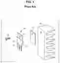
In regard to this, as a heat radiation structure, a package type power semiconductor device 10, an insulating pad 12, and a heat sink 14 are illustrated in FIG. 1. Here, a semiconductor chip is bonded to a metal tap 21 and is sealed using a sealing material 20 so that heat may be radiated through the heat sink 14 bonded to the insulating pad 12 interposed therebetween.
Accordingly, each semiconductor device needs a separate insulating pad or an insulating material applied thereto in order to combine with a heat sink.
Therefore, without applying of an insulating material to the heat sink, a technique to realize partial insulation is required in more economical way to combine with the heat sink.
SUMMARY OF THE INVENTION
The present invention provides a coupled semiconductor package where lower surfaces of one or more substrate pads are formed to be electrically connected and lower surfaces of another one or more substrate pads are formed to be electrically insulated so that insulation may be partly realized without applying of an insulating material to a heat sink, when the package is joined to the heat sink.
According to an aspect of the present invention, there is provided a coupled semiconductor package including: at least two substrate pads; at least one semiconductor chip installed on each of the substrate pads; at least one terminal each of which is electrically connected to each substrate pad and each semiconductor chip; and a package housing covering a part of the at least one semiconductor chip and the at least one terminal, wherein lower surfaces of one or more substrate pads are formed to be electrically connected and lower surfaces of another one or more substrate pads are formed to be electrically insulated.
The lower surfaces of one or more substrate pads may be partly or entirely exposed to the outside of one surface of the package housing so as to be electrically connected and the lower surfaces of another one or more substrate pads may not be exposed to the outside of the package housing so as to be electrically insulated.
The substrate pads may be formed of a conductive metal.
One or more substrate pads may be formed of a conductive metal, the lower surfaces thereof may be partly or entirely exposed to the outside of one surface of the package housing so as to be electrically connected, another one or more substrate pads may be formed of an insulating substrate including an insulating layer formed thereon, and the lower surfaces of the insulating substrates may be partly or entirely exposed to the outside of one surface of the package housing so as to be electrically insulated.
The package housing may be formed of an epoxy molding compound (EMC).
Another one or more substrate pads may be formed of at least one metal layer, at least one insulating layer, and at least one metal layer, which are sequentially stacked.
The insulating layer may include ceramic (Al2O3), AlN, or Si3N4.
One or more substrate pads and one or more terminals may be formed of the same material and connected to each other as in one body.
One or more substrate pads and one or more terminals may be separately formed and connected to each other using ultrasonic welding, soldering, or laser welding.
The terminals may contain more than 40 weight % of Al with respect to the total weight of the terminals.
The package housing may include one or more penetration holes.
One or more substrate pads may include holes that correspond to one or more penetration holes.
The coupled semiconductor package may further include a heat sink combined using a connecting means which penetrates the penetration holes and the holes.
The lower surfaces of one or more substrate pads may be exposed to the outside of one surface of the package housing by more than 90% of the area of the lower surfaces of the substrate pads.
The at least one semiconductor chip and the at least one terminal may be formed of Au, Al, or Cu as a single material so as to be electrically connected to each other, or may be formed of a combined material including at least any one of Au, Al, and Cu so as to be electrically connected to each other.
The at least one semiconductor chip and the at least one terminal may be electrically connected to each other using a conductive wire.
The at least one semiconductor chip and the at least one terminal may be electrically connected to each other using a metal clip.
BRIEF DESCRIPTION OF THE DRAWINGS
The above and other features and advantages of the present invention will become more apparent by describing in detail exemplary embodiments thereof with reference to the attached drawings in which:
FIG. 1 illustrates a semiconductor package according to a conventional art;
FIGS. 2A and 2B illustrate a coupled semiconductor package according to a first embodiment of the present invention;
FIG. 3 is an exploded perspective view of the coupled semiconductor package of FIGS. 2A and 2B;
FIGS. 4A and 4B illustrate a coupled semiconductor package according to a second embodiment of the present invention;
FIG. 5 is an exploded perspective view of the coupled semiconductor package of FIGS. 4A and 4B;
FIGS. 6A and 6B illustrate a coupled semiconductor package according to a third embodiment of the present invention; and
FIGS. 7 and 8 are exploded perspective views of the coupled semiconductor package of FIGS. 6A and 6B.
DETAILED DESCRIPTION OF THE INVENTION
Hereinafter, the present invention will be described in more detail with reference to the accompanying drawings to be easily implemented by those of ordinary skill in the art. This invention may be embodied in many alternate forms and should not be construed as limited to only the exemplary embodiments set forth herein.
A coupled semiconductor package according to the present invention includes at least two substrate pads 110, at least one semiconductor chip 120 installed on each of the substrate pads 110, at least one terminal 130 each of which is electrically connected to each substrate pad 110 and each semiconductor chip 120, and a package housing 140 covering a part of the at least one semiconductor chip 120 and the at least one terminal 130. Here, lower surfaces of one or more substrate pads 110 are formed to be electrically connected and lower surfaces of another one or more substrate pads 110 are formed to be electrically insulated so that insulation may be partly realized without applying of an insulating material to a heat sink, when the package is joined to the heat sink.
Hereinafter, the coupled semiconductor package described above will be respectively described in first through third embodiments according to the structure classified by the type of the substrate pads 110 exposed to the outside of the package housing 140.
The coupled semiconductor package according to the first embodiment of the present invention is described in more detail below with reference to FIGS. 2A through 3.
Firstly, the substrate pads 110 are lead frames, where the semiconductor chips 120 are installed, and the at least two substrate pads 110 are separately molded in the package housing 140. Also, the lower surfaces of one or more substrate pads 110 are formed to be electrically connected and the lower surfaces of another one or more substrate pads 110 are formed to be electrically insulated.
As illustrated in FIG. 2B, the substrate pads 110 are formed of a conductive metal, the lower surfaces of one or more substrate pads 110 are exposed to the outside of one surface of the package housing 140 so as to be electrically connected, and the lower surfaces of another one or more substrate pads 110 are not exposed to the outside of the package housing 140 so as to be electrically insulated. Accordingly, insulation may be partly realized when the package is joined to a heat sink (not illustrated).
The lower surfaces of one or more substrate pads 110 may be partly or entirely exposed to the outside of the package housing 140. For example, more than 90% of the area of the lower surfaces of one or more substrate pads 110 is exposed to the outside of one surface of the package housing 140 so as to maximize heat radiation effect.
In this regard, when insulation of a heat sink is needed, a separate insulating material is not needed to be applied to the heat sink and thus, a process of manufacturing a semiconductor package may be simplified.
Next, one or more semiconductor chips 120 are installed on each of the substrate pads 110 by using a conductive adhesive interposed therebetween.
For reference, the conductive adhesive may contain more than 40% of Sn or more than 50% of Ag or Cu, however, the present invention is not limited thereto. Also, a silicon control rectifier (SCR), a power transistor, an insulated gate bipolar transistor (IGBT), a metal-oxide semiconductor field effect transistor (MOSFET), a power rectifier, a power regulator, or a power semiconductor including a combination thereof may be applied as the semiconductor chip 120.
Next, each of the terminals 130 is electrically connected to each of the substrate pads 110 and each of the semiconductor chips 120 and may include a first terminal 131 electrically connected to the substrate pad 110 and a second terminal 132 electrically connected to the semiconductor chip 120.
The first terminal 131, which is a lead terminal applying an electric signal to the substrate pad 110, is electrically connected to the substrate pad 110, wherein one or more substrate pads 110 and one or more terminals 130 may be formed of the same material and connected to each other as in one body. Also, one or more substrate pads 110 and one or more terminals 130 may be separately formed and connected to each other using ultrasonic welding, soldering, or laser welding.
Here, the terminals 130 may contain more than 40 weight % of Al with respect to the total weight of the terminals 130 so that weight lighting may be realized and conductivity may be improved.
In addition, one or more semiconductor chips 120 and one or more terminals 130 may be formed of Au, Al, or Cu as a single material and electrically connected to each other. Also, one or more semiconductor chips 120 and one or more terminals 130 may be formed of a combined material including at least any one of Au, Al, and Cu and electrically connected to each other. Here, electrical connection may be, for example, a wire.
Moreover, one or more semiconductor chips 120 and one or more terminals 130 may be electrically connected to each other through a metal clip and thus, electrical stability may be secured.
Next, the package housing 140 is an insulator for protecting a semiconductor circuit, partially covers one or more semiconductor chips 120 and one or more terminals 130, and may be formed of an epoxy molding compound (EMC). However, the present invention is not limited thereto and the package housing 140 may be formed of polyphenylene sulfide (PPS) or polybutylene terephthalate (PBT).
The package housing 140 includes at least one penetration hole 141 and the substrate pad 110 includes a hole 111 that corresponds to the penetration hole 141. Accordingly, the package housing 140, the substrate pad 110, and a heat sink may be combined to each other through screw tightening.
The coupled semiconductor package according to the second embodiment of the present invention is described in more detail below with reference to FIGS. 4A through 5.
Firstly, the substrate pads 110 are lead frames, where the semiconductor chips 120 are installed, and the at least two substrate pads 110 are separately molded in the package housing 140. Also, the lower surfaces of one or more substrate pads 110 are formed to be electrically connected and the lower surfaces of another one or more substrate pads 110 are formed to be electrically insulated.
As illustrated in FIG. 4B, one or more substrate pads 110 are formed of a conductive metal and the lower surfaces formed of the conductive metal are exposed to the outside of one surface of the package housing 140 so as to be electrically connected. Also, another one or more substrate pads 110 are formed of an insulating substrate, where an insulating layer 112 is formed, and the lower surfaces of the insulating substrates are exposed to the outside of one surface of the package housing 140 so as to be electrically insulated. Accordingly, insulation may be partly realized when the package is joined to a heat sink (not illustrated).
The lower surfaces of one or more substrate pads 110 may be partly or entirely exposed to the outside of the package housing 140. For example, more than 90% of the area of the lower surfaces of one or more substrate pads 110 is exposed to the outside of one surface of the package housing 140 so as to maximize heat radiation effect.
In this regard, when insulation of a heat sink is needed, a separate insulating material is not needed to be applied to the heat sink and thus, a process of manufacturing a semiconductor package may be simplified.
Next, one or more semiconductor chips 120 are installed on each of the substrate pads 110 by using a conductive adhesive interposed therebetween.
For reference, the conductive adhesive may contain more than 40% of Sn or more than 50% of Ag or Cu, however, the present invention is not limited thereto. Also, a silicon control rectifier (SCR), a power transistor, an insulated gate bipolar transistor (IGBT), a metal-oxide semiconductor field effect transistor (MOSFET), a power rectifier, a power regulator, or a power semiconductor including a combination thereof may be applied as the semiconductor chip 120.
Next, each of the terminals 130 is electrically connected to each of the substrate pads 110 and each of the semiconductor chips 120 and may include the first terminal 131 electrically connected to the substrate pad 110 and the second terminal 132 electrically connected to the semiconductor chip 120.
The first terminal 131, which is a lead terminal applying an electric signal to the substrate pad 110, is electrically connected to the substrate pad 110, wherein one or more substrate pads 110 and one or more terminals 130 may be formed of the same material and connected to each other as in one body. Also, one or more substrate pads 110 and one or more terminals 130 may be separately formed and connected to each other using ultrasonic welding, soldering, or laser welding.
Here, the terminals 130 may contain more than 40 weight % of Al with respect to the total weight of the terminals 130 so that weight lighting may be realized and conductivity may be improved.
In addition, one or more semiconductor chips 120 and one or more terminals 130 may be formed of Au, Al, or Cu as a single material and electrically connected to each other. Also, one or more semiconductor chips 120 and one or more terminals 130 may be formed of a combined material including at least any one of Au, Al, and Cu and electrically connected to each other. Here, electrical connection may be, for example, a wire.
Moreover, one or more semiconductor chips 120 and one or more terminals 130 may be electrically connected to each other through a metal clip and thus, electrical stability may be secured.
Next, the package housing 140 is an insulator for protecting a semiconductor circuit, partially covers one or more semiconductor chips 120 and one or more terminals 130, and may be formed of an EMC. However, the present invention is not limited thereto and the package housing 140 may be formed of PPS or PBT.
The package housing 140 includes at least one penetration hole 141 and the substrate pad 110 includes the hole 111 that corresponds to the penetration hole 141. Accordingly, the package housing 140, the substrate pad 110, and a heat sink may be combined to each other through screw tightening.
The coupled semiconductor package according to the third embodiment of the present invention is described in more detail below with reference to FIGS. 6A through 8.
Firstly, the substrate pads 110 are lead frames, where the semiconductor chips 120 are installed, and the at least two substrate pads 110 are separately molded in the package housing 140. Also, the lower surfaces of one or more substrate pads 110 are formed to be electrically connected and the lower surfaces of another one or more substrate pads 110 are formed to be electrically insulated.
That is, as illustrated in FIGS. 6B and 8, one or more substrate pads 110 are formed of a conductive metal and the lower surfaces formed of the conductive metal are exposed to the outside of one surface of the package housing 140 so as to be electrically connected. Also, another one or more substrate pads 110 are formed of a metal layer 110a, an insulating layer 110b, and a metal layer 110c, which are sequentially stacked, for example, a direct bonded copper substrate (DBC), and the lower surfaces of the substrate pads 110 are exposed to the outside of one surface of the package housing 140 so as to be electrically insulated. Accordingly, insulation may be partly realized when the package is joined to a heat sink (not illustrated).
Here, the insulating layer 110b includes ceramic (Al2O3), AlN, or Si3N4 and thereby, provides an insulating structure between the metal layer 110a and the metal layer 110c.
The lower surfaces of one or more substrate pads 110 may be partly or entirely exposed to the outside of the package housing 140. For example, more than 90% of the area of the lower surfaces of one or more substrate pads 110 is exposed to the outside of one surface of the package housing 140 so as to maximize heat radiation effect.
In this regard, when insulation of a heat sink is needed, a separate insulating material is not needed to be applied to the heat sink and thus, a process of manufacturing a semiconductor package may be simplified.
Next, one or more semiconductor chips 120 are installed on each of the substrate pads 110 by using a conductive adhesive interposed therebetween.
For reference, the conductive adhesive may contain more than 40% of Sn or more than 50% of Ag or Cu, however, the present invention is not limited thereto. Also, a silicon control rectifier (SCR), a power transistor, an insulated gate bipolar transistor (IGBT), a metal-oxide semiconductor field effect transistor (MOSFET), a power rectifier, a power regulator, or a power semiconductor including a combination thereof may be applied as the semiconductor chip 120.
Next, each of the terminals 130 is electrically connected to each of the substrate pads 110 and each of the semiconductor chips 120 and may include the first terminal 131 electrically connected to the substrate pad 110 and the second terminal 132 electrically connected to the semiconductor chip 120.
The first terminal 131, which is a lead terminal applying an electric signal to the substrate pad 110, is electrically connected to the substrate pad 110, wherein one or more substrate pads 110 and one or more terminals 130 may be formed of the same material and connected to each other as in one body. Also, one or more substrate pads 110 and one or more terminals 130 may be separately formed and connected to each other using ultrasonic welding, soldering, or laser welding.
Here, the terminals 130 may contain more than 40 weight % of Al with respect to the total weight of the terminals 130 so that weight lighting may be realized and conductivity may be improved.
In addition, one or more semiconductor chips 120 and one or more terminals 130 may be formed of Au, Al, or Cu as a single material and electrically connected to each other. Also, one or more semiconductor chips 120 and one or more terminals 130 may be formed of a combined material including at least any one of Au, Al, and Cu and electrically connected to each other. Here, electrical connection may be, for example, a wire.
Moreover, one or more semiconductor chips 120 and one or more terminals 130 may be electrically connected to each other through a metal clip and thus, electrical stability may be secured.
Next, the package housing 140 is an insulator for protecting a semiconductor circuit, partially covers one or more semiconductor chips 120 and one or more terminals 130, and may be formed of an epoxy molding compound (EMC). However, the present invention is not limited thereto and the package housing 140 may be formed of a polyphenylene sulfide (PPS) or polybutylene terephthalate (PBT).
The package housing 140 includes at least one penetration hole 141 and the substrate pad 110 includes the hole 111 that corresponds to the penetration hole 141. Accordingly, the package housing 140, the substrate pad 110, and a heat sink may be combined to each other through screw tightening.
According to the coupled semiconductor package described above, at least two substrate pads are molded in the package housing having a single structure, wherein a part of the substrate pads is exposed and the other part of the substrate pads is not exposed. Accordingly, partial insulation may be economically realized without applying an insulating material to the heat sink, when the package is joined to the heat sink. Also, a part of the substrate pads is formed of an insulating substrate or a DBC substrate and thereby, at least two substrate pads are exposed so that partial insulation may be economically realized without applying an insulating material to the heat sink, when the package is joined to the heat sink.
According to the present invention, at least two substrate pads are molded in the package housing having a single structure, wherein a part of the substrate pads is exposed and the other part of the substrate pads is not exposed. Accordingly, partial insulation may be economically realized without applying an insulating material to the heat sink, when the package is joined to the heat sink.
In addition, a part of the substrate pads is formed of an insulating substrate or a DBC substrate and thereby, at least two substrate pads are exposed so that partial insulation may be economically realized without applying an insulating material to the heat sink.
While the present invention has been particularly shown and described with reference to exemplary embodiments thereof, it will be understood by those of ordinary skill in the art that various changes in form and details may be made therein without departing from the spirit and scope of the present invention as defined by the following claims.
Claims
What is claimed is:1. A coupled semiconductor package comprising:
at least two substrate pads;
at least one semiconductor chip installed on each of the substrate pads;
at least one terminal each of which is electrically connected to each substrate pad and each semiconductor chip; and
a package housing covering a part of the at least one semiconductor chip and the at least one terminal,
wherein lower surfaces of one or more substrate pads are formed to be electrically connected and lower surfaces of another one or more substrate pads are formed to be electrically insulated.
2. The coupled semiconductor package of claim 1, wherein the lower surfaces of one or more substrate pads are partly or entirely exposed to the outside of one surface of the package housing so as to be electrically connected and the lower surfaces of another one or more substrate pads are not exposed to the outside of the package housing so as to be electrically insulated.
3. The coupled semiconductor package of claim 2, wherein the substrate pads are formed of a conductive metal.
4. The coupled semiconductor package of claim 1, wherein one or more substrate pads are formed of a conductive metal, the lower surfaces thereof are partly or entirely exposed to the outside of one surface of the package housing so as to be electrically connected, another one or more substrate pads are formed of an insulating substrate including an insulating layer formed thereon, and the lower surfaces of the insulating substrates are partly or entirely exposed to the outside of one surface of the package housing so as to be electrically insulated.
5. The coupled semiconductor package of claim 1, wherein the package housing is formed of an epoxy molding compound (EMC).
6. The coupled semiconductor package of claim 1, wherein another one or more substrate pads are formed of at least one metal layer, at least one insulating layer, and at least one metal layer, which are sequentially stacked.
7. The coupled semiconductor package of claim 6, wherein the insulating layer includes ceramic (Al2O3), AlN, or Si3N4.
8. The coupled semiconductor package of claim 1, wherein one or more substrate pads and one or more terminals are formed of the same material and connected to each other as in one body.
9. The coupled semiconductor package of claim 1, wherein one or more substrate pads and one or more terminals are separately formed and connected to each other using ultrasonic welding, soldering, or laser welding.
10. The coupled semiconductor package of claim 1, wherein the terminals contain more than 40 weight % of Al with respect to the total weight of the terminals.
11. The coupled semiconductor package of claim 1, wherein the package housing includes one or more penetration holes.
12. The coupled semiconductor package of claim 11, wherein one or more substrate pads include holes that correspond to one or more penetration holes.
13. The coupled semiconductor package of claim 12, further comprising a heat sink combined using a connecting means which penetrates the penetration holes and the holes.
14. The coupled semiconductor package of claim 1, wherein the lower surfaces of one or more substrate pads are exposed to the outside of one surface of the package housing by more than 90% of the area of the lower surfaces of the substrate pads.
15. The coupled semiconductor package of claim 1, wherein the at least one semiconductor chip and the at least one terminal are formed of Au, Al, or Cu as a single material so as to be electrically connected to each other, or formed of a combined material including at least any one of Au, Al, and Cu so as to be electrically connected to each other.
16. The coupled semiconductor package of claim 1, wherein the at least one semiconductor chip and the at least one terminal are electrically connected to each other using a conductive wire.
17. The coupled semiconductor package of claim 1, wherein the at least one semiconductor chip and the at least one terminal are electrically connected to each other using a metal clip.
Images & Drawings included:


Sources:
- United States Patent and Trademark Office - verify current appl. status at the USPTO↗
Similar patent applications:
- » 20090113698
Apparatus for electrically coupling a semiconductor package to a printed circuit board - » 10759990
Semiconductor package with substrate coupled to a peripheral side surface of a semiconductor die - » 20230369160
Semiconductor Device Package Thermally Coupled to Passive Element - » 20200105718
Semiconductor packages with chiplets coupled to a memory device - » 20230273367
Semiconductor package comprising optically coupled IC chips - » 20230361093
Semiconductor Device Package with Coupled Substrates - » 20190103385
Thermally coupled package-on-package semiconductor packages - » 20190305428
Antenna structure with integrated coupling element and semiconductor package using the same - » 20230197682
Semiconductor packages with chiplets coupled to a memory device - » 20240203851
Semiconductor Device Package with Coupled Substrates
Recent applications in this class:
- » 20250293125 2025-09-18
SEMICONDUCTOR DEVICE - » 20250210472 2025-06-26
SEMICONDUCTOR PACKAGE, POWER SEMICONDUCTOR MODULE AND MANUFACTURING PROCESS - » 20250149409 2025-05-08
SEMICONDUCTOR DEVICE - » 20250022778 2025-01-16
SEMICONDUCTOR MODULE - » 20240332136 2024-10-03
POWER SEMICONDUCTOR DEVICE WITH A STRESS-FREE JOINT BETWEEN METAL PARTS AND METHOD FOR FABRICATING THE SAME - » 20240258209 2024-08-01
SEMICONDUCTOR DEVICE - » 20240203837 2024-06-20
Packaged stackable electronic power device for surface mounting and circuit arrangement - » 20230402349 2023-12-14
METHOD OF MANUFACTURING SEMICONDUCTOR DEVICES AND CORRESPONDING SEMICONDUCTOR DEVICE HAVING VIAS AND PADS FORMED BY LASER - » 20230282553 2023-09-07
POWER ELECTRONIC ASSEMBLY AND POWER MODULE FOR EMBEDDING IN A PRINTED CIRCUIT BOARD - » 20230275006 2023-08-31
SEMICONDUCTOR APPARATUS
Recent applications for this Assignee:
- » 20250174521 2025-05-29
SEMICONDUCTOR PACKAGE INCLUDING HEAT RADIATION STRUCTURE, COOLING SYSTEM APPLYING THE SEMICONDUCTOR PACKAGE, SUBSTRATE INCLUDING HEAT RADIATION STRUCTURE AND METHOD OF MANUFACTURING THE SUBSTRATE - » 20230268252 2023-08-24
SEMICONDUCTOR PACKAGE INCLUDING HEAT RADIATION STRUCTURE, COOLING SYSTEM APPLYING THE SEMICONDUCTOR PACKAGE, SUBSTRATE INCLUDING HEAT RADIATION STRUCTURE AND METHOD OF MANUFACTURING THE SUBSTRATE - » 20230011694 2023-01-12
SEMICONDUCTOR PACKAGE HAVING PACKAGE HOUSING IN ENGRAVED SURFACE FORM AND METHOD OF MANUFACTURING THE SAME - » 20220399300 2022-12-15
CLIP STRUCTURE FOR SEMICONDUCTOR PACKAGE AND SEMICONDUCTOR PACKAGE INCLUDING THE SAME - » 20220359452 2022-11-10
Semiconductor package, method of manufacturing the same and metal bridge applied to the semiconductor package - » 20220285304 2022-09-08
Semiconductor package and method of manufacturing the same - » 20220246494 2022-08-04
System for cooling semiconductor component, method of manufacturing the same, and semiconductor package having the system - » 20220223504 2022-07-14
Plurality of power semiconductor chips between a substrate and leadframe - » 20220148998 2022-05-12
Semiconductor package - » 20210366799 2021-11-25
Semiconductor package and method of manufacturing the same