LIGHT-EMITTING DEVICE INCLUDING ORGANOMETALLIC COMPOUND, ELECTRONIC DEVICE INCLUDING THE LIGHT-EMITTING DEVICE, AND THE ORGANOMETALLIC COMPOUND
US20240174705A1
2024-05-30
18/321,910
2023-05-23
Smart Summary: A new type of light-emitting device uses a special chemical called an organometallic compound. This device has two electrodes, one on each side, with a layer in between that produces light. The organometallic compound plays a key role in making the light. Additionally, this light-emitting device can be part of larger electronic devices. Overall, it offers a new way to create light for various applications. 🚀 TL;DR
Abstract:
Embodiments provide a light-emitting device including an organometallic compound, and an electronic device including the light-emitting device. The light-emitting device includes a first electrode, a second electrode facing the first electrode, an interlayer between the first electrode and the second electrode and including an emission layer, and the organometallic compound. The organometallic compound is represented by Formula 1, which is explained in the specification:
Inventors:
- Eunyoung Lee 83 🇰🇷 Yongin-si, South Korea
- Junghoon Han 85 🇰🇷 Yongin-si, South Korea
- Sungbum KIM 104 🇰🇷 Yongin-si, South Korea
- Iljoon Kang 35 🇰🇷 Yongin-si, South Korea
- Sujin SHIN 77 🇰🇷 Yongin-si, South Korea
- Hyunjung LEE 69 🇰🇷 Yongin-si, South Korea
Assignee:
- SAMSUNG DISPLAY CO., LTD. 14,186 🇰🇷 Yongin-si, South Korea
Applicant:
Interested in similar patents?
Get notified when new applications in this technology area are published.
Classification:
C07F15/0086 » CPC main
Compounds containing elements of Groups 8, 9, 10 or 18 of the Periodic System compounds of the platinum group Platinum compounds
C09K11/06 » CPC further
Luminescent, e.g. electroluminescent, chemiluminescent materials containing organic luminescent materials
C07B2200/05 » CPC further
Indexing scheme relating to specific properties of organic compounds Isotopically modified compounds, e.g. labelled
C07F15/00 IPC
Compounds containing elements of Groups 8, 9, 10 or 18 of the Periodic System
Description
CROSS-REFERENCE TO RELATED APPLICATION(S)
This application claims priority to and benefits of Korean Patent Application No. 10-2022-0142463 under 35 U.S.C. § 119, filed on Oct. 31, 2022, in the Korean Intellectual Property Office, the entire contents of which are incorporated herein by reference herein.
BACKGROUND
1. Technical Field
Embodiments relate to a light-emitting device including an organometallic compound, an electronic device including the light-emitting device, and the organometallic compound.
2. Description of the Related Art
From among light-emitting devices, self-emissive devices have wide viewing angles, high contrast ratios, short response times, and excellent characteristics in terms of luminance, driving voltage, and response speed.
In a light-emitting device, a first electrode is located on a substrate, and a hole transport region, an emission layer, an electron transport region, and a second electrode are sequentially arranged on the first electrode. Holes provided from the first electrode move toward the emission layer through the hole transport region, and electrons provided from the second electrode move toward the emission layer through the electron transport region. Carriers, such as holes and electrons, recombine in the emission layer to produce excitons. These excitons transition from an excited state to a ground state to thereby generate light.
It is to be understood that this background of the technology section is, in part, intended to provide useful background for understanding the technology. However, this background of the technology section may also include ideas, concepts, or recognitions that were not part of what was known or appreciated by those skilled in the pertinent art prior to a corresponding effective filing date of the subject matter disclosed herein.
SUMMARY
Embodiments include a light-emitting device including an organometallic compound, an electronic device including the light-emitting device, and the organometallic compound.
Additional aspects will be set forth in part in the description which follows and, in part, will be apparent from the description, or may be learned by practice of the embodiments of the disclosure.
According to embodiments, a light-emitting device may include a first electrode, a second electrode facing the first electrode, and an interlayer between the first electrode and the second electrode and including an emission layer, and an organometallic compound represented by Formula 1:
In Formula 1,
-
- M may be platinum (Pt), palladium (Pd), cobalt (Co), gold (Au), nickel (Ni), silver (Ag), or copper (Cu),
- A1 to A5 may each independently be a C3-C60 carbocyclic group unsubstituted or substituted with at least one R10a or a C1-C60 heterocyclic group unsubstituted or substituted with at least one R10a,
- at least one of A4 and A5 may be a C8-C60 polycyclic group unsubstituted or substituted with at least one R10a,
- the C8-C60 polycyclic group may be a condensed ring in which four or more C2-C6 monocyclic groups are condensed with each other,
- X1 to X4 may each independently be C or N,
- L1 to L3 may each independently be a single bond, *—N(R51)—*′, *—B(R51)—*′, *—P(R51)—*′, *—C(R51)(R52)—*′, *—Si(R51)(R52)—*′, *—Ge(R51)(R52)—*′, *—S—*′, *—Se—*′, *—O—*′, *—C(═O)—*′, *—S(═O)—*′, *—S(═O)2—*′ or *—C(═S)—*′,
- n1 to n3 may each independently be an integer from 1 to 4,
- a1 to a5 may each independently be an integer from 1 to 6,
- R1 to R5 may each independently be hydrogen, deuterium, —F, —Cl, —Br, —I, a hydroxyl group, a cyano group, a nitro group, a C1-C60 alkyl group unsubstituted or substituted with at least one R10a, a C2-C60 alkenyl group unsubstituted or substituted with at least one R10a, a C2-C60 alkynyl group unsubstituted or substituted with at least one R10a, a C1-C60 alkoxy group unsubstituted or substituted with at least one R10a, a C3-C60 carbocyclic group unsubstituted or substituted with at least one R10a, a C1-C60 heterocyclic group unsubstituted or substituted with at least one R10a, —C(Q1)(Q2)(Q3), —Si(Q1)(Q2)(Q3), —N(Q1)(Q2), —B(Q1)(Q2), —C(═O)(Q1), —S(═O)2(Q1), or —P(═O)(Q1)(Q2),
- R10a may be:
- deuterium, —F, —Cl, —Br, —I, a hydroxyl group, a cyano group, or a nitro group,
- a C1-C60 alkyl group, a C2-C60 alkenyl group, a C2-C60 alkynyl group, or a C1-C60 alkoxy group, each unsubstituted or substituted with deuterium, —F, —Cl, —Br, —I, a hydroxyl group, a cyano group, a nitro group, a C3-C60 carbocyclic group, a C1-C60 heterocyclic group, a C6-C60 aryloxy group, a C6-C60 arylthio group, a C7-C60 arylalkyl group, a C2-C60 heteroarylalkyl group, —Si(Q11)(Q12)(Q13), —N(Q11)(Q12), —B(Q11)(Q12), —C(═O)(Q11), —S(═O)2(Q11), —P(═O)(Q11)(Q12), or any combination thereof;
- a C3-C60 carbocyclic group, a C1-C60 heterocyclic group, a C6-C60 aryloxy group, a C6-C60 arylthio group, a C7-C60 arylalkyl group, or a C2-C60 heteroarylalkyl group, each unsubstituted or substituted with deuterium, —F, —Cl, —Br, —I, a hydroxyl group, a cyano group, a nitro group, a C1-C60 alkyl group, a C2-C60 alkenyl group, a C2-C60 alkynyl group, a C1-C60 alkoxy group, a C3-C60 carbocyclic group, a C1-C60 heterocyclic group, a C6-C60 aryloxy group, a C6-C60 arylthio group, a C7-C60 arylalkyl group, a C2-C60 heteroarylalkyl group, —Si(Q21)(Q22)(Q23), —N(Q21)(Q22), —B(Q21)(Q22), —C(═O)(Q21), —S(═O)2(Q21), —P(═O)(Q21)(Q22), or any combination thereof; or
- —Si(Q31)(Q32)(Q33), —N(Q31)(Q32), —B(Q31)(Q32), —C(═O)(Q31), —S(═O)2(Q31), or —P(═O)(Q31)(Q32), and
- Q1 to Q3, Q11 to Q13, Q21 to Q23, and Q31 to Q33 may each independently be hydrogen, deuterium, —F, —Cl, —Br, —I, a hydroxyl group, a cyano group, a nitro group, or a C1-C60 alkyl group, a C2-C60 alkenyl group, a C2-C60 alkynyl group, a C1-C60 alkoxy group, a C3-C60 carbocyclic group, or a C1-C60 heterocyclic group, each unsubstituted or substituted with deuterium, —F, a cyano group, a C1-C60 alkyl group, a C1-C60 alkoxy group, a phenyl group, a biphenyl group, or any combination thereof.
In an embodiment, the first electrode may be an anode,
-
- the second electrode may be a cathode,
- the interlayer may further include a hole transport region between the first electrode and the emission layer, and an electron transport region between the emission layer and the second electrode,
- the hole transport region may include a hole injection layer, a hole transport layer, an emission auxiliary layer, an electron-blocking layer, or any combination thereof, and
- the electron transport region may include a hole-blocking layer, an electron transport layer, an electron injection layer, an electron control layer, or any combination thereof.
In an embodiment, the interlayer may include the organometallic compound.
In an embodiment, emission layer may include the organometallic compound.
In an embodiment, the organometallic compound included in the emission layer may be a phosphorescent dopant.
Embodiments provide an electronic device which may include the light-emitting device.
In an embodiment, the electronic device may further include a color filter, a color conversion layer, a touch screen layer, a polarizing layer, or any combination thereof.
Embodiments provide an electronic apparatus which may include the light-emitting device.
In an embodiment, the electronic apparatus may be a flat panel display, a curved display, a computer monitor, a medical monitor, a television, a billboard, an indoor light, an outdoor light, a signal light, a head-up display, a fully transparent display, a partially transparent display, a flexible display, a rollable display, a foldable display, a stretchable display, a laser printer, a telephone, a portable phone, a tablet personal computer, a phablet, a personal digital assistant (PDA), a wearable device, a laptop computer, a digital camera, a camcorder, a viewfinder, a micro display, a three-dimensional (3D) display, a virtual reality, an augmented reality display, a vehicle, a video wall with multiple displays tiled together, a theater screen, a stadium screen, a phototherapy device, or a signboard.
Embodiments provide an organometallic compound which may be represented by Formula 1, which is described herein.
In an embodiment, M may be platinum (Pt).
In an embodiment, A1 to A5 may each independently be a benzene group, a pentalene group, a naphthalene group, an azulene group, an indacene group, an acenaphthylene group, a phenalene group, a phenanthrene group, an anthracene group, a fluoranthene group, a triphenylene group, a pyrene group, a chrysene group, a pyrrole group, an indole group, a benzoindole group, a naphthoindole group, an iso-indole group, a benzoiso-indole group, a naphthoiso-indole group, a carbazole group, an indenocarbazole group, an indolocarbazole group, a benzoindolocarbazole group, a benzocarbazole group, a pyrazole group, an imidazole group, a triazole group, a benzopyrazole group, a benzimidazole group, an indazole group, a pyridine group, a pyrimidine group, a pyrazine group, a pyridazine group, a triazine group, a quinoline group, an isoquinoline group, a benzoquinoline group, a benzoisoquinoline group, a quinoxaline group, a benzoquinoxaline group, a quinazoline group, a benzoquinazoline group, a phenanthroline group, a cinnoline group, a phthalazine group, a naphthyridine group, an imidazopyridine group, an imidazopyrimidine group, an imidazotriazine group, an imidazopyrazine group, an imidazopyridazine group, an azacarbazole group, or an azafluorene group.
In an embodiment, A5 may be a C8-C60 polycyclic group unsubstituted or substituted with at least one R10a.
In an embodiment, the C2-C6 monocyclic group may be a 5-membered ring or a 6-membered ring,
the 5-membered ring may be a cyclopentane group, a cyclopentene group, a pyrrole group, a pyrazole group, an imidazole group, or a triazole group, and
-
- the 6-membered ring may be a cyclohexane group, a cyclohexene group, a benzene group, a pyridine group, a pyrimidine group, a pyrazine group, a pyridazine group, or a triazine group.
In an embodiment, the C8-C60 polycyclic group may be a condensed ring in which two or more 5-membered rings and two or more 6-membered rings may be condensed with each other,
-
- the two or more 5-membered rings may include two pyrrole groups, and
- the two pyrrole groups may be condensed with each other sharing a nitrogen atom.
In an embodiment, X2 may be C, and
-
- a bond between X2 and M may be a coordinate bond.
In an embodiment, L1 may be *—O—*′, and
-
- L2 and L3 may each be a single bond.
In an embodiment, R1 to R5 may each independently be:
-
- hydrogen, deuterium, —F, —Cl, —Br, —I, a cyano group, or a C1-C20 alkyl group;
- a C1-C20 alkyl group unsubstituted or substituted with at least one of deuterium, —F, —Cl, —Br, —I, —CDs, —CD2H, —CDH2, —CF3, —CF2H, —CFH2, a cyano group, a nitro group, a C1-C10 alkyl group, a cyclopentyl group, a cyclohexyl group, a cycloheptyl group, a cyclooctyl group, an adamantanyl group, a norbornanyl group, a norbornenyl group, a cyclopentenyl group, a cyclohexenyl group, a cycloheptenyl group, a phenyl group, a biphenyl group, a naphthyl group, a pyridinyl group, or a pyrimidinyl group;
- a phenyl group, a pyridine group, a dibenzofuranyl group, a dibenzothiophenyl group, a carbazolyl group, an azadibenzofuranyl group, an azadibenzothiophenyl group, or an azacarbazolyl group, each unsubstituted or substituted with at least one of deuterium, —F, —Cl, —Br, —I, —CDs, —CD2H, —CDH2, —CF3, —CF2H, —CFH2, a cyano group, a C1-C20 alkyl group, a phenyl group, a biphenyl group, a C1-C10 alkylphenyl group, a naphthyl group, a fluorenyl group, a phenanthrenyl group, an anthracenyl group, a fluoranthenyl group, a triphenylenyl group, a pyrenyl group, a chrysenyl group, a pyrrolyl group, a thiophenyl group, a furanyl group, an imidazolyl group, a pyrazolyl group, a thiazolyl group, an isothiazolyl group, an oxazolyl group, an isoxazolyl group, a pyridinyl group, a pyrazinyl group, a pyrimidinyl group, a pyridazinyl group, an isoindolyl group, an indolyl group, an indazolyl group, a purinyl group, a quinolinyl group, an isoquinolinyl group, a benzoquinolinyl group, a quinoxalinyl group, a quinazolinyl group, a cinnolinyl group, a carbazolyl group, a phenanthrolinyl group, a benzoimidazolyl group, a benzofuranyl group, a benzothiophenyl group, a benzoisothiazolyl group, a benzoxazolyl group, an isobenzoxazolyl group, a triazolyl group, a tetrazolyl group, an oxadiazolyl group, a triazinyl group, a dibenzofuranyl group, a dibenzothiophenyl group, a benzocarbazolyl group, a dibenzocarbazolyl group, an imidazopyridinyl group, an imidazopyrimidinyl group, —Si(Q31)(Q32)(Q33), —N(Q31)(Q32), or —B(Q31)(Q32); or
- —Si(Q1)(Q2)(Q3), —N(Q1)(Q2), or —B(Q1)(Q2), and
- Q1 to Q3 and Q31 to Q33 may each independently be:
- —CH3, —CD3, —CD2H, —CDH2, —CH2CH3, —CH2CD3, —CH2CD2H, —CH2CDH2, —CHDCH3, —CHDCD2H, —CHDCDH2, —CHDCD3, —CD2CD3, —CD2CD2H, or —CD2CDH2; or
- an n-propyl group, an isopropyl group, an n-butyl group, an isobutyl group, a sec-butyl group, a tert-butyl group, an n-pentyl group, an isopentyl group, a sec-pentyl group, a tert-pentyl group, a phenyl group, a naphthyl group, a pyridinyl group, a pyrimidinyl group, a pyridazinyl group, a pyrazinyl group, or a triazinyl group, each unsubstituted or substituted with at least one of deuterium, a C1-C10 alkyl group, a phenyl group, a biphenyl group, a pyridinyl group, a pyrimidinyl group, a pyridazinyl group, a pyrazinyl group, and a triazinyl group.
In an embodiment, in Formula 1, a moiety represented by
may be a moiety represented by one of Formulae 2-1 to 2-8, which are explained below.
In an embodiment, the organometallic compound represented by Formula 1 may be one of Compounds 1 to 140, which are explained below
It is to be understood that the embodiments above are described in a generic and explanatory sense only and not for the purpose of limitation, and the disclosure is not limited to the embodiments described above.
BRIEF DESCRIPTION OF THE DRAWINGS
The above and other aspects and features of the disclosure will be more apparent by describing in detail embodiments thereof with reference to the accompanying drawings, in which:
FIG. 1 is a schematic cross-sectional view of a light-emitting device according to an embodiment;
FIG. 2 is a schematic cross-sectional view of an electronic device according to an embodiment;
FIG. 3 is a schematic cross-sectional view of an electronic device according to another embodiment;
FIG. 4 is a schematic perspective view of an electronic apparatus according to an embodiment;
FIG. 5 is a schematic perspective view of the exterior of a vehicle as an electronic apparatus according to an embodiment; and
FIGS. 6A to 6C are each a schematic diagram of an interior of a vehicle as an electronic apparatus according to an embodiment.
DETAILED DESCRIPTION OF THE EMBODIMENTS
The disclosure will now be described more fully hereinafter with reference to the accompanying drawings, in which embodiments are shown. This disclosure may, however, be embodied in different forms and should not be construed as limited to the embodiments set forth herein. Rather, these embodiments are provided so that this disclosure will be thorough and complete, and will fully convey the scope of the disclosure to those skilled in the art.
In the drawings, the sizes, thicknesses, ratios, and dimensions of the elements may be exaggerated for ease of description and for clarity. Like reference numbers and/or like reference characters refer to like elements throughout.
In the description, it will be understood that when an element (or region, layer, part, etc.) is referred to as being “on”, “connected to”, or “coupled to” another element, it can be directly on, connected to, or coupled to the other element, or one or more intervening elements may be present therebetween. In a similar sense, when an element (or region, layer, part, etc.) is described as “covering” another element, it can directly cover the other element, or one or more intervening elements may be present therebetween.
In the description, when an element is “directly on,” “directly connected to,” or “directly coupled to” another element, there are no intervening elements present. For example, “directly on” may mean that two layers or two elements are disposed without an additional element such as an adhesion element therebetween.
It will be understood that the terms “connected to” or “coupled to” may refer to a physical, electrical and/or fluid connection or coupling, with or without intervening elements.
As used herein, the expressions used in the singular such as “a,” “an,” and “the,” are intended to include the plural forms as well, unless the context clearly indicates otherwise.
As used herein, the term “and/or” includes any and all combinations of one or more of the associated listed items. For example, “A and/or B” may be understood to mean “A, B, or A and B.” The terms “and” and “or” may be used in the conjunctive or disjunctive sense and may be understood to be equivalent to “and/or”.
In the specification and the claims, the term “at least one of” is intended to include the meaning of “at least one selected from the group of” for the purpose of its meaning and interpretation. For example, “at least one of A and B” may be understood to mean “A, B, or A and B.” When preceding a list of elements, the term, “at least one of,” modifies the entire list of elements and does not modify the individual elements of the list.
It will be understood that, although the terms first, second, etc. may be used herein to describe various elements, these elements should not be limited by these terms. These terms are only used to distinguish one element from another element. Thus, a first element could be termed a second element without departing from the teachings of the disclosure. Similarly, a second element could be termed a first element, without departing from the scope of the disclosure.
The spatially relative terms “below”, “beneath”, “lower”, “above”, “upper”, or the like, may be used herein for ease of description to describe the relations between one element or component and another element or component as illustrated in the drawings. It will be understood that the spatially relative terms are intended to encompass different orientations of the device in use or operation, in addition to the orientation depicted in the drawings. For example, in the case where a device illustrated in the drawing is turned over, the device positioned “below” or “beneath” another device may be placed “above” another device. Accordingly, the illustrative term “below” may include both the lower and upper positions. The device may also be oriented in other directions and thus the spatially relative terms may be interpreted differently depending on the orientations.
The terms “about” or “approximately” as used herein is inclusive of the stated value and means within an acceptable range of deviation for the recited value as determined by one of ordinary skill in the art, considering the measurement in question and the error associated with measurement of the recited quantity (i.e., the limitations of the measurement system). For example, “about” may mean within one or more standard deviations, or within +20%, 10%, or ±5% of the stated value.
It should be understood that the terms “comprises,” “comprising,” “includes,” “including,” “have,” “having,” “contains,” “containing,” and the like are intended to specify the presence of stated features, integers, steps, operations, elements, components, or combinations thereof in the disclosure, but do not preclude the presence or addition of one or more other features, integers, steps, operations, elements, components, or combinations thereof.
Unless otherwise defined or implied herein, all terms (including technical and scientific terms) used have the same meaning as commonly understood by those skilled in the art to which this disclosure pertains. It will be further understood that terms, such as those defined in commonly used dictionaries, should be interpreted as having a meaning that is consistent with their meaning in the context of the relevant art and should not be interpreted in an ideal or excessively formal sense unless clearly defined in the specification.
A light-emitting device may include: a first electrode; a second electrode facing the first electrode; an interlayer between the first electrode and the second electrode and including an emission layer; and an organometallic compound represented by Formula 1:
In Formula 1, M may be platinum (Pt), palladium (Pd), gold (Au), nickel (Ni), silver (Ag), or copper (Cu).
In an embodiment, M may be platinum (Pt).
In Formula 1, A1 to A5 may each independently be a C3-C60 carbocyclic group unsubstituted or substituted with at least one R10a or a C1-C60 heterocyclic group unsubstituted or substituted with at least one R10a.
For example, A1 to A5 may each independently be a cyclopentadiene group, an adamantane group, a norbornane group, a benzene group, a pentalene group, a naphthalene group, an azulene group, an indacene group, an acenaphthylene group, a phenalene group, a phenanthrene group, an anthracene group, a fluoranthene group, a triphenylene group, a pyrene group, a chrysene group, a perylene group, a pentaphene group, a heptalene group, a naphthacene group, a picene group, a hexacene group, a pentacene group, a rubicene group, a coronene group, an ovalene group, an indene group, a fluorene group, a spiro-bitluorene group, a benzofluorene group, an indeno phenanthrene group, an indenoanthracene group, a pyrrole group, a thiophene group, a furan group, an indole group, a benzoindole group, a naphthonindole group, an iso-indole group, a benzoiso-indole group, a naphthoiso-indole group, a benzosilole group, a benzothiophene group, a benzofuran group, a carbazole group, a dibenzosilole group, a dibenzothiophene group, a dibenzofuran group, an indenocarbazole group, an indolocarbazole group, a benzofurocarbazole group, a benzothienocarbazole group, a benzosilolocarbazole group, a benzoindolocarbazole group, a benzocarbazole group, a benzonaphthofuran group, a benzonaphthothiophene group, a benzonaphthosilole group, a benzofurodibenzofuran group, a benzofurodibenzothiophene group, a benzothienodibenzothiophene group, a pyrazole group, an imidazole group, a triazole group, an oxazole group, an isoxazole group, an oxadiazole group, a thiazole group, an isothiazole group, a thiadiazole group, a benzopyrazole group, a benzimidazole group, a benzoxazole group, a benzoisoxazole group, a benzothiazole group, a benzoisothiazole group, an indazole group, a pyridine group, a pyrimidine group, a pyrazine group, a pyridazine group, a triazine group, a quinoline group, an isoquinoline group, a benzoquinoline group, a benzoisoquinoline group, a quinoxaline group, a benzoquinoxaline group, a quinazoline group, a benzoquinazoline group, a phenanthroline group, a cinnoline group, a phthalazine group, a naphthyridine group, an imidazopyridine group, an imidazopyrimidine group, an imidazotriazine group, an imidazopyrazine group, an imidazopyridazine group, an azacarbazole group, an azafluorene group, an azadibenzosilole group, an azadibenzothiophene group, or an azadibenzofuran group.
In an embodiment, A1 to A5 may each independently be a benzene group, a pentalene group, a naphthalene group, an azulene group, an indacene group, an acenaphthylene group, a phenalene group, a phenanthrene group, an anthracene group, a fluoranthene group, a triphenylene group, a pyrene group, a chrysene group, a pyrrole group, an indole group, a benzoindole group, a naphthoindole group, an iso-indole group, a benzoiso-indole group, a naphthoiso-indole group, a carbazole group, an indenocarbazole group, an indolocarbazole group, a benzoindolocarbazole group, a benzocarbazole group, a pyrazole group, an imidazole group, a triazole group, a benzopyrazole group, a benzimidazole group, an indazole group, a pyridine group, a pyrimidine group, a pyrazine group, a pyridazine group, a triazine group, a quinoline group, an isoquinoline group, a benzoquinoline group, a benzoisoquinoline group, a quinoxaline group, a benzoquinoxaline group, a quinazoline group, a benzoquinazoline group, a phenanthroline group, a cinnoline group, a phthalazine group, a naphthyridine group, an imidazopyridine group, an imidazopyrimidine group, an imidazotriazine group, an imidazopyrazine group, an imidazopyridazine group, an azacarbazole group, or an azafluorene group, and the indolocarbazole group may include indolo[3,2,1-jk]carbazole.
In Formula 1, at least one of A4 and A5 may be a C8-C60 polycyclic group unsubstituted or substituted with at least one R10a, and
the C8-C60 polycyclic group may be a condensed ring in which four or more C2-C6 monocyclic groups are condensed with each other.
In an embodiment, A5 may be a C8-C60 polycyclic group unsubstituted or substituted with at least one R10a.
The C8-C60 polycyclic group may be a condensed ring in which four to six C2-C6 monocyclic groups are condensed with each other, and for example, the C8-C60 polycyclic group may a condensed ring in which five or more C2-C6 monocyclic groups are condensed with each other.
In an embodiment, the C2-C6 monocyclic group may be a 5-membered ring or a 6-membered ring,
-
- the 5-membered ring may be a cyclopentane group, a cyclopentene group, a pyrrole group, a pyrazole group, an imidazole group, or a triazole group, and
- the 6-membered ring may be a cyclohexane group, a cyclohexene group, a benzene group, a pyridine group, a pyrimidine group, a pyrazine group, a pyridazine group, or a triazine group.
In an embodiment, the C8-C60 polycyclic group may be a condensed ring in which two or more 5-membered rings and two or more 6-membered rings are condensed with each other.
In an embodiment, the C8-C60 polycyclic group may be a condensed ring in which two or more 5-membered rings and two or more 6-membered rings are condensed with each other, wherein the two or more 5-membered rings include two pyrrole groups, and the two pyrrole groups are condensed with each other sharing a nitrogen atom.
In Formula 1, X1 to X4 may each independently be C or N.
For example, X1, X2, and X4 may each be C, X3 may be N. In an embodiment, X2 may be C, and a bond between X2 and M may be a coordinate bond.
In Formula 1, L1 to L3 may each independently be a single bond, *—N(R51)—*′, *—B(R51)—*′, *-β(R51)—*′, *—C(R51)(R52)—*′, *—Si(R51)(R52)—*′, *—Ge(R51)(R52)—*′, *—S—*′, *—Se—*′, *—O—*′, *—C(═O)—*′, *—S(═O)—*′, *—S(═O)2—*′, or *—C(═S)—*′.
In an embodiment, L1 may be *—O—*′, L2 and L3 may each be a single bond.
In Formula 1, n1 to n3 may each independently be an integer from 1 to 4. In an embodiment, n1 to n3 may each independently be 1 or 2.
In Formula 1, a1 to a5 may each independently be an integer from 1 to 6. In an embodiment, a1 to a5 may each independently be an integer from 1 to 3.
In Formula 1, R1 to R5 may each independently be hydrogen, deuterium, —F, —Cl, —Br, —I, a hydroxyl group, a cyano group, a nitro group, a C1-C60 alkyl group unsubstituted or substituted with at least one R10a, a C2-C60 alkenyl group unsubstituted or substituted with at least one R10a, a C2-C60 alkynyl group unsubstituted or substituted with at least one R10a, a C1-C60 alkoxy group unsubstituted or substituted with at least one R10a, a C3-C60 carbocyclic group unsubstituted or substituted with at least one R10a, a C1-C60 heterocyclic group unsubstituted or substituted with at least one R10a, —C(Q1)(Q2)(Q3), —Si(Q1)(Q2)(Q3), —N(Q1)(Q2), —B(Q1)(Q2), —C(═O)(Q1), —S(═O)2(Q1), or —P(═O)(Q1)(Q2),
-
- R10a may be:
- deuterium, —F, —Cl, —Br, —I, a hydroxyl group, a cyano group, or a nitro group;
- a C1-C60 alkyl group, a C2-C60 alkenyl group, a C2-C60 alkynyl group, or a C1-C60 alkoxy group, each unsubstituted or substituted with deuterium, —F, —Cl, —Br, —I, a hydroxyl group, a cyano group, a nitro group, a C3-C60 carbocyclic group, a C1-C60 heterocyclic group, a C6-C60 aryloxy group, a C6-C60 arylthio group, a C7-C60 arylalkyl group, a C2-C60 heteroarylalkyl group, —Si(Q11)(Q12)(Q13), —N(Q11)(Q12), —B(Q11)(Q12), —C(═O)(Q11), —S(═O)2(Q11), —P(═O)(Q11)(Q12), or any combination thereof;
- a C3-C60 carbocyclic group, a C1-C60 heterocyclic group, a C6-C60 aryloxy group, a C6-C60 arylthio group, a C7-C60 arylalkyl group, or a C2-C60 heteroarylalkyl group, each unsubstituted or substituted with deuterium, —F, —CI, —Br, —I, a hydroxyl group, a cyano group, a nitro group, a C1-C60 alkyl group, a C2-C60 alkenyl group, a C2-C60 alkynyl group, a C1-C60 alkoxy group, a C3-C60 carbocyclic group, a C1-C60 heterocyclic group, a C6-C60 aryloxy group, a C6-C60 arylthio group, a C7-C60 arylalkyl group, a C2-C60 heteroarylalkyl group, —Si(Q21)(Q22)(Q23), —N(Q21)(Q22), —B(Q21)(Q22), —C(═O)(Q21), —S(═O)2(Q21), —P(═O)(Q21)(Q22), or any combination thereof; or
- —Si(Q31)(Q32)(Q33), —N(Q31)(Q32), —B(Q31)(Q32), —C(═O)(Q31), —S(═O)2(Q31), or —P(═O)(Q31)(Q32), and
- Q1 to Q3, Q11 to Q13, Q21 to Q23, and Q31 to Q33 may each independently be: hydrogen; deuterium; —F; —Cl; —Br; —I; a hydroxyl group; a cyano group; a nitro group; or a C1-C60 alkyl group, a C2-C60 alkenyl group, a C2-C60 alkynyl group, a C1-C60 alkoxy group, a C3-C60 carbocyclic group, or a C1-C60 heterocyclic group, each unsubstituted or substituted with deuterium, —F, a cyano group, a C1-C60 alkyl group, a C1-C60 alkoxy group, a phenyl group, a biphenyl group, or any combination thereof.
For example, R1 to R5 may each independently be
-
- hydrogen, deuterium, —F, a cyano group, a C1-C20 alkyl group unsubstituted or substituted with at least one R10a, a C2-C6 monocyclic group unsubstituted or substituted with at least one R10a, or a C4-C13 polycyclic group unsubstituted or substituted with at least one R10a.
For example, R1 to R5 may each independently be:
-
- hydrogen, deuterium, —F, or a cyano group;
- a C1-C20 alkyl group unsubstituted or substituted with hydrogen, deuterium, —F, a cyano group, or any combination thereof; or
- a benzene group, a pyridine group, a dibenzofuran group, a dibenzothiophene group, a carbazole group, an azadibenzofuran group, an azadibenzothiophene group, or an azacarbazole group, each unsubstituted or substituted with hydrogen, deuterium, —F, a cyano group, a C1-C20 alkyl group, a deuterated C1-C20 alkyl group, a fluorinated C1-C20 alkyl group, a phenyl group, a deuterated phenyl group, a fluorinated phenyl group, a (C1-C20 alkyl)phenyl group, a biphenyl group, a dibenzofuranyl group, a dibenzothiophenyl group, a carbazolyl group, a fluorenyl group, a dibenzosilolyl group, or any combination thereof.
In an embodiment, R1 to R5 may each independently be:
-
- hydrogen, deuterium, —F, —Cl, —Br, —I, a cyano group, or a C1-C20 alkyl group;
- a C1-C20 alkyl group unsubstituted or substituted with at least one of deuterium, —F, —Cl, —Br, —I, —CD3, —CD2H, —CDH2, —CF3, —CF2H, —CFH2, a cyano group, a nitro group, a C1-C10 alkyl group, a cyclopentyl group, a cyclohexyl group, a cycloheptyl group, a cyclooctyl group, an adamantanyl group, a norbornanyl group, a norbornenyl group, a cyclopentenyl group, a cyclohexenyl group, a cycloheptenyl group, a phenyl group, a biphenyl group, a naphthyl group, a pyridinyl group, or a pyrimidinyl group;
- a phenyl group, a pyridine group, a dibenzofuranyl group, a dibenzothiophenyl group, a carbazolyl group, an azadibenzofuranyl group, an azadibenzothiophenyl group, or an azacarbazolyl group, each unsubstituted or substituted with at least one of deuterium, —F, —Cl, —Br, —I, —CD3, —CD2H, —CDH2, —CF3, —CF2H, —CFH2, a cyano group, a C1-C20 alkyl group, a phenyl group, a biphenyl group, a C1-C1 alkylphenyl group, a naphthyl group, a fluorenyl group, a phenanthrenyl group, an anthracenyl group, a fluoranthenyl group, a triphenylenyl group, a pyrenyl group, a chrysenyl group, a pyrrolyl group, a thiophenyl group, a furanyl group, an imidazolyl group, a pyrazolyl group, a thiazolyl group, an isothiazolyl group, an oxazolyl group, an isoxazolyl group, a pyridinyl group, a pyrazinyl group, a pyrimidinyl group, a pyridazinyl group, an isoindolyl group, an indolyl group, an indazolyl group, a purinyl group, a quinolinyl group, an isoquinolinyl group, a benzoquinolinyl group, a quinoxalinyl group, a quinazolinyl group, a cinnolinyl group, a carbazolyl group, a phenanthrolinyl group, a benzoimidazolyl group, a benzofuranyl group, a benzothiophenyl group, a benzoisothiazolyl group, a benzoxazolyl group, an isobenzoxazolyl group, a triazolyl group, a tetrazolyl group, an oxadiazolyl group, a triazinyl group, a dibenzofuranyl group, a dibenzothiophenyl group, a benzocarbazolyl group, a dibenzocarbazolyl group, an imidazopyridinyl group, an imidazopyrimidinyl group, —Si(Q31)(Q32)(Q33), —N(Q31)(Q32), or —B(Q31)(Q32); or
- —Si(Q1)(Q2)(Q3), —N(Q1)(Q2), or —B(Q1)(Q2), and
- Q1 to Q3 and Q31 to Q33 may each independently be:
- —CH3, —CD3, —CD2H, —CDH2, —CH2CH3, —CH2CD3, —CH2CD2H, —CH2CDH2, —CHDCH3, —CHDCD2H, —CHDCDH2, —CHDCD3, —CD2CD3, —CD2CD2H, or —CD2CDH2; or
- an n-propyl group, an iso-propyl group, an n-butyl group, an isobutyl group, a sec-butyl group, a tert-butyl group, an n-pentyl group, an isopentyl group, a sec-pentyl group, a tert-pentyl group, a phenyl group, a naphthyl group, a pyridinyl group, a pyrimidinyl group, a pyridazinyl group, a pyrazinyl group, or a triazinyl group, each unsubstituted or substituted with at least one of deuterium, a C1-C10 alkyl group, a phenyl group, a biphenyl group, a pyridinyl group, a pyrimidinyl group, a pyridazinyl group, a pyrazinyl group, and a triazinyl group.
In an embodiment, R1 to R5 may each independently be:
-
- a methyl group, an ethyl group, an n-propyl group, an iso-propyl group, an n-butyl group, an isobutyl group, a sec-butyl group, a tert-butyl group, an n-pentyl group, an isopentyl group, a sec-pentyl group, a tert-pentyl group, a 2-methylbutyl group, a 2-2dimethylpropyl group, a 1-ethylpropyl group, or a 1,2-dimethylpropyl group, each unsubstituted or substituted with deuterium, —F, —Cl, —Br, —I, a hydroxyl group, a cyano group, or a nitro group; or
- a benzene group, a pyridine group, a dibenzofuran group, a dibenzothiophene group, a carbazole group, an azadibenzofuran group, an azadibenzothiophene group, or an azacarbazole group, each unsubstituted or substituted with a methyl group, an ethyl group, an n-propyl group, an iso-propyl group, an n-butyl group, an isobutyl group, a sec-butyl group, a tert-butyl group, an n-pentyl group, an isopentyl group, a sec-pentyl group, a tert-pentyl group, a 2-methylbutyl group, a 2-2dimethylpropyl group, 1-ethylpropyl group, 1,2-dimethylpropyl group, or phenyl group, each unsubstituted or substituted with deuterium, —F, —Cl, —Br, —I, a hydroxyl group, a cyano group, or a nitro group.
In an embodiment, in Formula 1, a moiety represented by
may be a moiety represented by one of Formulae 2-1 to 2-8:
In Formulae 2-1 to 2-8,
-
- X41 may be C(R41) or N, X42 may be C(R42) or N, X43 may be C(R43) or N, X44 may be C(R44) or N, X45 may be C(R45) or N, X46 may be C(R46) or N, X47 may be C(R47) or N, X48 may be C(R48) or N, X49 may be C(R49) or N, X410 may be C(R410) or N, and X411 may be C(R411) or N,
- R41 to R49, R410, and R411 may each independently be the same as described herein in connection with R4 in Formula 1, and
- *, *′, and *″ may respectively indicate a binding side to M, L1, and L3.
In an embodiment, in Formula 1, A2 may be a moiety represented by Formula 3:
In Formula 3,
-
- A21 may be the same as described herein in connection with A2,
- R21 and R22 may each independently be the same as described herein in connection with R1 to R5,
- a21 may be the same as described herein in connection with a1 to a5, and
- * and *′ may respectively indicate a binding site to M and L2.
In an embodiment, the organometallic compound represented by Formula 1 may be one of Compounds 1 to 140:
The organometallic compound represented by Formula 1 may include ring A4 and ring A5, at least one of ring A4 and ring A5 may be a C8-C60 polycyclic group unsubstituted or substituted with at least one R10a, and the C8-C60 polycyclic group may be a condensed ring in which four or more C2-C6 monocyclic groups are condensed with each other.
As such, the organometallic compound represented by Formula 1 may include a condensed ring in which four or more rings are condensed as a ligand bonded to a metal, and accordingly, rigidity of the ligand may be improved, which leads to relatively excellent light-emission characteristics. Therefore, an electronic device (for example, an organic light-emitting device) with high efficiency and long lifespan may be implemented by using the organometallic compound.
Methods of synthesizing the organometallic compound represented by Formula 1 may be readily understood to those of ordinary skill in the art by referring to Synthesis Examples and/or Examples described herein.
At least one organometallic compound represented by Formula 1 may be utilized in a light-emitting device (for example, an organic light-emitting device). In an embodiment, a light-emitting device may include: a first electrode; a second electrode facing the first electrode; and an interlayer located between the first electrode and the second electrode and including an emission layer, wherein the interlayer includes the organometallic compound represented by Formula 1.
In embodiments,
-
- the first electrode of the light-emitting device may be an anode,
- the second electrode of the light-emitting device may be a cathode,
- the interlayer may further include a hole transport region between the first electrode and the emission layer, and an electron transport region between the emission layer and the second electrode,
- the hole transport region may include a hole injection layer, a hole transport layer, an emission auxiliary layer, an electron-blocking layer, or any combination thereof, and
- the electron transport region may include a hole-blocking layer, an electron transport layer, an electron injection layer, an electron control layer, or any combination thereof.
In embodiments, the interlayer of the light-emitting device may include the organometallic compound represented by Formula 1.
In embodiments, the emission layer of the light-emitting device may include the organometallic compound represented by Formula 1.
In embodiments, the emission layer may emit blue light. For example, the emission layer may emit blue light having a maximum emission wavelength in a range of about 400 nm to about 500 nm. For example, the emission layer may emit blue light having a maximum emission wavelength in a range of about 410 nm to about 490 nm. For example, the emission layer may emit blue light having a maximum emission wavelength in a range of about 420 nm to about 480 nm. For example, the emission layer may emit blue light having a maximum emission wavelength in a range of about 430 nm to about 470 nm.
In embodiments, the emission layer of the light-emitting device may include a dopant and a host, and the organometallic compound represented by Formula 1 may be included in the dopant. For example, the organometallic compound may serve as a dopant.
In embodiments, the organometallic compound may be a phosphorescent dopant.
In embodiments, the electron transport region of the light-emitting device may include a hole-blocking layer, and the hole-blocking layer may include a phosphine oxide-containing compound, a silicon-containing compound, or any combination thereof. In an embodiment, the hole-blocking layer may contact (e.g., directly contact) the emission layer.
In an embodiment, the light-emitting device may include a capping layer located outside the first electrode or outside the second electrode.
In an embodiment, the light-emitting device may further include at least one of a first capping layer located outside the first electrode and a second capping layer located outside the second electrode, and the organometallic compound represented by Formula 1 may be included in at least one of the first capping layer and the second capping layer. The first capping layer and/or the second capping layer may be the same as described in the specification.
In an embodiment, the light-emitting device may further include:
-
- a first capping layer located outside the first electrode and including the organometallic compound represented by Formula 1;
- a second capping layer located outside the second electrode and including the organometallic compound represented by Formula 1; or
- the first capping layer and the second capping layer.
The wording “(interlayer and/or capping layer) includes an organometallic compound” as used herein may be understood as “(interlayer and/or capping layer) may include one kind of organometallic compound represented by Formula 1 or two different kinds of organometallic compounds, each represented by Formula 1”.
For example, the interlayer and/or capping layer may include Compound 1 only as the organometallic compound. In this regard, Compound 1 may be present in the emission layer of the light-emitting device. In embodiments, the interlayer may include, as the organometallic compound, Compound 1 and Compound 2. In this regard, Compound 1 and Compound 2 may be present in the same layer (for example, all of Compound 1 and Compound 2 may be present in the emission layer), or may be present in different layers (for example, Compound 1 may be present in the emission layer, and Compound 2 may be present in the electron transport region).
The term “interlayer” as used herein refers to a single layer and/or all layers between a first electrode and a second electrode of a light-emitting device.
In an embodiment, the emission layer may further include a first host and a second host, wherein the first host may be an electron-transporting host and the second host may be a hole-transporting host.
In an embodiment, the first host may include at least one azine moiety, and the second host may include at least one carbazole moiety.
In an embodiment, the first host may include a compound represented by Formula 5:
In Formula 5,
-
- X54 to X56 may each independently be C(R50), CH, or N, and at least one of X54 to X56 may each be N,
- ring CY51 to ring CY53 may each independently include a C5-C60 carbocyclic group or a C1-C60 heterocyclic group,
- L51 to L53 may each independently include a C3-C60 carbocyclic group unsubstituted or substituted with at least one R10a or a C1-C60 heterocyclic group unsubstituted or substituted with at least one R10a,
- b51 to b53 may each independently be an integer from 0 to 3,
- when b51 is 0, *-(L51)b51-*′ may be a single bond,
- when b52 is 0, *-(L52)b52-*′ may be a single bond,
- when b53 is 0, *-(L53)ab3-*′ may be a single bond,
- R50 to R53 may each independently be the same as described herein in connection with R1 to R5, and
- a51 to a53 may each independently be an integer from 0 to 10.
In an embodiment, in Formula 5, ring CY51 to ring CY53 may each independently include: a first ring; a second ring; a condensed ring in which at least two first rings are condensed; a condensed ring in which at least two second rings are condensed; or a condensed ring in which at least one first ring is condensed with at least one second ring,
-
- the first ring may include a cyclopentadiene group, an adamantane group, a norbornane group, a benzene group, a pentalene group, a naphthalene group, an azulene group, an indacene group, an acenaphthylene group, a phenalene group, a phenanthrene group, an anthracene group, a fluoranthene group, a triphenylene group, a pyrene group, a chrysene group, a perylene group, a pentaphene group, a heptalene group, a naphthacene group, a picene group, a hexacene group, a pentacene group, a rubicene group, a coronene group, an ovalene group, an indene group, a fluorene group, a spiro-bifluorene group, a benzofluorene group, an indenophenanthrene group, or an indenoanthracene group, and
- the second ring may include a pyrrole group, a thiophene group, a furan group, an indole group, a benzoindole group, a naphthoindole group, an isoindole group, a benzoisoindole group, a naphthoisoindole group, a benzosilole group, a benzothiophene group, a benzofuran group, a carbazole group, a dibenzosilole group, a dibenzothiophene group, a dibenzofuran group, an indenocarbazole group, an indolocarbazole group, a benzofurocarbazole group, a benzothienocarbazole group, a benzosilolocarbazole group, a benzoindolocarbazole group, a benzocarbazole group, a benzonaphthofuran group, a benzonaphthothiophene group, a benzonaphthosilole group, a benzofurodibenzofuran group, a benzofurodibenzothiophene group, a benzothienodibenzothiophene group, a pyrazole group, an imidazole group, a triazole group, an oxazole group, an isoxazole group, an oxadiazole group, a thiazole group, an isothiazole group, a thiadiazole group, a benzopyrazole group, a benzimidazole group, a benzoxazole group, a benzoisoxazole group, a benzothiazole group, a benzoisothiazole group, a pyridine group, a pyrimidine group, a pyrazine group, a pyridazine group, a triazine group, a quinoline group, an isoquinoline group, a benzoquinoline group, a benzoisoquinoline group, a quinoxaline group, a benzoquinoxaline group, a quinazoline group, a benzoquinazoline group, a phenanthroline group, a cinnoline group, a phthalazine group, a naphthyridine group, an imidazopyridine group, an imidazopyrimidine group, an imidazotriazine group, an imidazopyrazine group, an imidazopyridazine group, an azacarbazole group, an azafluorene group, an azadibenzosilole group, an azadibenzothiophene group, or an azadibenzofuran group.
In an embodiment, in Formula 5, CY51 to CY53 may each independently include a benzene group, a naphthalene group, an anthracene group, a phenanthrene group, a triphenylene group, a pyrene group, a chrysene group, a cyclopentadiene group, a 1,2,3,4-tetrahydronaphthalene group, a thiophene group, a furan group, an indole group, a benzoborole group, a benzophosphole group, an indene group, a benzosilole group, a benzogermole group, a benzothiophene group, a benzoselenophene group, a benzofuran group, a carbazole group, a dibenzoborole group, a dibenzophosphole group, a fluorene group, a dibenzosilole group, a dibenzogermole group, a dibenzothiophene group, a dibenzoselenophene group, a dibenzofuran group, a dibenzothiophene 5-oxide group, 9H-fluorene-9-one group, a dibenzothiophene 5,5-dioxide group, an azaindole group, an azabenzoborole group, an azabenzophosphole group, an azaindene group, an azabenzosilole group, an azabenzogermole group, an azabenzothiophene group, an azabenzoselenophene group, an azabenzofuran group, an azacarbazole group, an azadibenzoborole group, an azadibenzophosphole group, an azafluorene group, an azadibenzosilole group, an azadibenzogermole group, an azadibenzothiophene group, an azadibenzoselenophene group, an azadibenzofuran group, an azadibenzothiophene 5-oxide group, an aza-9H-fluorene-9-one group, an azadibenzothiophene 5,5-dioxide group, a pyridine group, a pyrimidine group, a pyrazine group, a pyridazine group, a triazine group, a quinoline group, an isoquinoline group, a quinoxaline group, a quinazoline group, a phenanthroline group, a pyrrole group, a pyrazole group, an imidazole group, a triazole group, an oxazole group, an iso-oxazole group, a thiazole group, an isothiazole group, an oxadiazole group, a thiadiazole group, a benzopyrazole group, a benzimidazole group, a benzoxazole group, a benzothiazole group, a benzoxadiazole group, a benzothiadiazole group, a 5,6,7,8-tetrahydroisoquinoline group, or a 5,6,7,8-tetrahydroquinoline group.
In an embodiment, in Formula 5, L51 to L53 may each independently include a benzene group, a naphthalene group, an anthracene group, a phenanthrene group, a triphenylene group, a pyrene group, a chrysene group, cyclopentadiene group, a furan group, a thiophene group, a silole group, an indene group, a fluorene group, an indole group, a carbazole group, a benzofuran group, a dibenzofuran group, a benzothiophene group, a dibenzothiophene group, a benzosilole group, a dibenzosilole group, an azafluorene group, an azacarbazole group, an azadibenzofuran group, an azadibenzothiophene group, an azadibenzosilole group, a pyridine group, a pyrimidine group, a pyrazine group, a pyridazine group, a triazine group, a quinoline group, an isoquinoline group, a quinoxaline group, a quinazoline group, a phenanthroline group, a pyrrole group, a pyrazole group, an imidazole group, a triazole group, an oxazole group, an isooxazole group, a thiazole group, an isothiazole group, an oxadiazole group, a thiadiazole group, a benzopyrazole group, a benzimidazole group, a benzoxazole group, a benzothiazole group, a benzoxadiazole group, or a benzothiadiazole group.
In an embodiment, the first host may include at least one compound selected from Compounds ETH1 to ETH32:
In an embodiment, the first host may include Compound ETH66:
In an embodiment, the second host may include a compound represented by Formula 7:
In Formula 7,
-
- ring CY71 and ring CY72 may each independently include a C5-C60 carbocyclic group or a C1-C60 heterocyclic group,
- X81 may be a single bond, O, S, N(R81), B(R81), C(R81a)(R81b), or Si(R81a)(R81b),
- R71, R72, R81, R81a, and R81b may each independently be the same as described herein in connection with R1 to R5, and
- a71 and a72 may each independently be an integer from 0 to 10.
In an embodiment, in Formula 7, ring CY71 and ring CY72 may each independently include: a first ring; a second ring; a condensed ring in which at least two first rings are condensed; a condensed ring in which at least two second rings are condensed; or a condensed ring in which at least one first ring is condensed with at least one second ring, and
-
- the first ring may include a cyclopentadiene group, an adamantane group, a norbornane group, a benzene group, a pentalene group, a naphthalene group, an azulene group, an indacene group, an acenaphthylene group, a phenalene group, a phenanthrene group, an anthracene group, a fluoranthene group, a triphenylene group, a pyrene group, a chrysene group, a perylene group, a pentaphene group, a heptalene group, a naphthacene group, a picene group, a hexacene group, a pentacene group, a rubicene group, a coronene group, an ovalene group, an indene group, a fluorene group, a spiro-bifluorene group, a benzofluorene group, an indenophenanthrene group, or an indenoanthracene group, and
- the second ring may include a pyrrole group, a thiophene group, a furan group, an indole group, a benzoindole group, a naphthoindole group, an isoindole group, a benzoisoindole group, a naphthoisoindole group, a benzosilole group, a benzothiophene group, a benzofuran group, a carbazole group, a dibenzosilole group, a dibenzothiophene group, a dibenzofuran group, an indenocarbazole group, an indolocarbazole group, a benzofurocarbazole group, a benzothienocarbazole group, a benzosilolocarbazole group, a benzoindolocarbazole group, a benzocarbazole group, a benzonaphthofuran group, a benzonaphthothiophene group, a benzonaphthosilole group, a benzofurodibenzofuran group, a benzofurodibenzothiophene group, a benzothienodibenzothiophene group, a pyrazole group, an imidazole group, a triazole group, an oxazole group, an isoxazole group, an oxadiazole group, a thiazole group, an isothiazole group, a thiadiazole group, a benzopyrazole group, a benzimidazole group, a benzoxazole group, a benzoisoxazole group, a benzothiazole group, a benzoisothiazole group, a pyridine group, a pyrimidine group, a pyrazine group, a pyridazine group, a triazine group, a quinoline group, an isoquinoline group, a benzoquinoline group, a benzoisoquinoline group, a quinoxaline group, a benzoquinoxaline group, a quinazoline group, a benzoquinazoline group, a phenanthroline group, a cinnoline group, a phthalazine group, a naphthyridine group, an imidazopyridine group, an imidazopyrimidine group, an imidazotriazine group, an imidazopyrazine group, an imidazopyridazine group, an azacarbazole group, an azafluorene group, an azadibenzosilole group, an azadibenzothiophene group, or an azadibenzofuran group.
In an embodiment, in Formula 7, CY71 to CY72 may each independently include a benzene group, a naphthalene group, an anthracene group, a phenanthrene group, a triphenylene group, a pyrene group, a chrysene group, a cyclopentadiene group, a 1,2,3,4-tetrahydronaphthalene group, a thiophene group, a furan group, an indole group, a benzoborole group, a benzophosphole group, an indene group, a benzosilole group, a benzogermole group, a benzothiophene group, a benzoselenophene group, a benzofuran group, a carbazole group, a dibenzoborole group, a dibenzophosphole group, a fluorene group, a dibenzosilole group, a dibenzogermole group, a dibenzothiophene group, a dibenzoselenophene group, a dibenzofuran group, a dibenzothiophene 5-oxide group, 9H-fluorene-9-one group, a dibenzothiophene 5,5-dioxide group, an azaindole group, an azabenzoborole group, an azabenzophosphole group, an azaindene group, an azabenzosilole group, an azabenzogermole group, an azabenzothiophene group, an azabenzoselenophene group, an azabenzofuran group, an azacarbazole group, an azadibenzoborole group, an azadibenzophosphole group, an azafluorene group, an azadibenzosilole group, an azadibenzogermole group, an azadibenzothiophene group, an azadibenzoselenophene group, an azadibenzofuran group, an azadibenzothiophene 5-oxide group, an aza-9H-fluorene-9-one group, an azadibenzothiophene 5,5-dioxide group, a pyridine group, a pyrimidine group, a pyrazine group, a pyridazine group, a triazine group, a quinoline group, an isoquinoline group, a quinoxaline group, a quinazoline group, a phenanthroline group, a pyrrole group, a pyrazole group, an imidazole group, a triazole group, an oxazole group, an iso-oxazole group, a thiazole group, an isothiazole group, an oxadiazole group, a thiadiazole group, a benzopyrazole group, a benzimidazole group, a benzoxazole group, a benzothiazole group, a benzoxadiazole group, a benzothiadiazole group, a 5,6,7,8-tetrahydroisoquinoline group, or a 5,6,7,8-tetrahydroquinoline group.
In an embodiment, the second host may include a compound represented by one of Formulae 7-1 to 7-5:
In Formulae 7-1 to 7-5,
-
- ring CY71, ring CY72, X81, R71, R72, a71, and a72 may be the same as described herein,
- ring CY73, ring CY74, R73, R74, a73, and a74 may respectively be the same as described herein in connection with ring CY71, ring CY72, R71, R72, a71, and a72,
- L81 and L82 may each independently be selected from *—C(Q4)(Q5)-*′, *—Si(Q4)(Q5)-*′, a substituted or unsubstituted C5-C30 carbocyclic group, and a substituted or unsubstituted C1-C30 heterocyclic group, and Q4 and Q5 may each independently be the same as described herein in connection with Q1,
- b81 and b82 may each be an integer from 0 to 5, wherein when b81 is 0, *-(L81)b81-*′ may be a single bond; when b81 is 2 or more, two or more of L81(s) may be identical to or different from each other; when b82 is 0, *-(L82)b82-*′ may be a single bond; and when b82 is 2 or more, two or more of L82(s) may be identical to or different from each other,
- X82 may be a single bond, O, S, N(R82), B(R82), C(R82a)(R82b), or Si(R82a)(R82b),
- X83 may be a single bond, O, S, N(R83), B(R83), C(R83a)(R83b), or Si(R83a)(R83b),
- in Formulae 7-2 and 7-4, X82 and X83 may each not be a single bond,
- X84 may be C or Si,
- R80, R82, R83, R82a, R82b, R83a, R83b, and R84 may each independently be the same as described in connection with R81, and
- * and *′ each indicate a binding site to a neighboring atom.
In embodiments,
-
- a moiety represented by
in Formulae 7-1 and 7-2 may be a moiety represented by one of Formulae CY71-1(1) to CY71-1(8),
-
- a moiety represented by
in Formulae 7-1 and 7-3 may be a moiety represented by one of Formulae CY71-2(1) to CY71-2(8),
-
- a moiety represented by
in Formulae 7-2 and 7-4 may be a moiety represented by one of Formulae CY71-3(1) to CY71-3(32),
-
- a moiety represented by
in Formulae 7-3 to 7-5 may be a moiety represented by one of Formulae CY71-4(1) to CY71-4(32), and
-
- a moiety represented by
in Formula 7-5 may be a moiety represented by one of Formulae CY71-5(1) to CY71-5(8):
In Formulae CY71-1(1) to CY71-1(8), CY71-2(1) to CY71-2(8), CY71-3(1) to CY71-3(32), CY71-4(1) to CY71-4(32), and CY71-5(1) to CY71-5(8),
-
- X81 to X84, R80, and R84 may be the same as described in the specification,
- X85 may be a single bond, O, S, N(R85), B(R85), C(R85a)(R85b), or Si(R85a)(R85b),
- X86 may be a single bond, O, S, N(R86), B(R86), C(R86a)(R86b), or Si(R86a)(R86b),
- in Formulae CY71-1(1) to CY71-1(8) and CY71-4(1) to CY71-4(32), X85 and X86 may each not be a single bond at the same time,
- X87 may be a single bond, O, S, N(R87), B(R87), C(R87a)(R87b), or Si(R87a)(R87b),
- X88 may be a single bond, O, S, N(R88), B(R88), C(R88a)(R88b), or Si(R88a)(R88b),
- in Formulae CY71-2(1) to CY71-2(8), CY71-3(1) to CY71-3(32) and CY71-5(1) to CY71-5(8), X87 and X88 may each not be a single bond at the same time, and
- R85 to R88, R85a, R85b, R86a, R86b, R87a, R87b, R88a, and R88b may each independently be the same as described in connection with R81.
In an embodiment, the second host may include at least one compound selected from Compounds HTH1 to HTH40:
In an embodiment, the second host may include Compound HTH29.
In the light-emitting device according to an embodiment, the first host and the second host may form an exciplex, and the organometallic compound and the first host or the organometallic compound and the second host may not form an exciplex.
Another aspect provides an electronic device including the light-emitting device. The electronic device may further include a thin-film transistor. For example, the electronic device may further include a thin-film transistor including a source electrode and a drain electrode, wherein the first electrode of the light-emitting device may be electrically connected to the source electrode or the drain electrode. In an embodiment, the electronic device may further include a color filter, a color conversion layer, a touch screen layer, a polarizing layer, or any combination thereof. The electronic device may be the same as described in the specification.
[Description of FIG. 1]
FIG. 1 is a schematic cross-sectional view of a light-emitting device 10 according to an embodiment. The light-emitting device 10 includes a first electrode 110, an interlayer 130, and a second electrode 150.
Hereinafter, the structure of the light-emitting device 10 according to an embodiment and a method of manufacturing the light-emitting device 10 will be described with reference to FIG. 1.
[First Electrode 110]
In FIG. 1, a substrate may be further included under the first electrode 110 or on the second electrode 150. The substrate may be a glass substrate or a plastic substrate but is not limited thereto. In embodiments, the substrate may be a flexible substrate, and may include plastics with excellent heat resistance and durability, such as polyimide, polyethylene terephthalate (PET), polycarbonate, polyethylene naphthalate, polyarylate (PAR), polyetherimide, or any combination thereof.
The first electrode 110 may be formed by, for example, depositing or sputtering a material for forming the first electrode 110 on the substrate. When the first electrode 110 is an anode, a material for forming the first electrode 110 may be a high-work function material that facilitates injection of holes.
The first electrode 110 may be a reflective electrode, a semi-transmissive electrode, or a transmissive electrode. When the first electrode 110 is a transmissive electrode, a material for forming the first electrode 110 may include indium tin oxide (ITO), indium zinc oxide (IZO), tin oxide (SnO2), zinc oxide (ZnO), or any combination thereof. In embodiments, when the first electrode 110 is a semi-transmissive electrode or a reflective electrode, a material for forming the first electrode 110 may include magnesium (Mg), silver (Ag), aluminum (Al), aluminum-lithium (Al—Li), calcium (Ca), magnesium-indium (Mg—In), magnesium-silver (Mg—Ag), or any combination thereof.
The first electrode 110 may have a structure consisting of a single layer or a structure including multiple layers. For example, the first electrode 110 may have a three-layered structure of ITO/Ag/ITO.
[Interlayer 130]
The interlayer 130 may be located on the first electrode 110. The interlayer 130 may include an emission layer.
The interlayer 130 may further include a hole transport region between the first electrode 110 and the emission layer, and an electron transport region between the emission layer and the second electrode 150.
The interlayer 130 may further include, in addition to various organic materials, a metal-containing compound such as an organometallic compound, an inorganic material such as quantum dots, or the like.
In embodiments, the interlayer 130 may include two or more emitting units stacked between the first electrode 110 and the second electrode 150, and at least one charge generation layer between the two or more emitting units. When the interlayer 130 includes emitting units and the at least one charge generation layer as described above, the light-emitting device 10 may be a tandem light-emitting device.
[Hole Transport Region in Interlayer 130]
The hole transport region may have: a structure consisting of a layer consisting of a single material, a structure consisting of a layer including different materials, or a structure including multiple layers including different materials.
The hole transport region may include a hole injection layer, a hole transport layer, an emission auxiliary layer, an electron-blocking layer, or any combination thereof.
For example, the hole transport region may have a multi-layered structure including a hole injection layer/hole transport layer structure, a hole injection layer/hole transport layer/emission auxiliary layer structure, a hole injection layer/emission auxiliary layer structure, a hole transport layer/emission auxiliary layer structure, or a hole injection layer/hole transport layer/electron-blocking layer structure, wherein the layers of each structure may be stacked from the first electrode 110 in its respective stated order, but the structure of the hole transport region is not limited thereto.
The hole transport region may include a compound represented by Formula 201, a compound represented by Formula 202, or any combination thereof:
In Formulae 201 and 202,
-
- L201 to L204 may each independently be a C3-C60 carbocyclic group unsubstituted or substituted with at least one R10a or a C1-C60 heterocyclic group unsubstituted or substituted with at least one R10a,
- L205 may be *—O—*′, *—S—*′, *—N(Q201)-*′, a C1-C20 alkylene group unsubstituted or substituted with at least one R10a, a C2-C20 alkenylene group unsubstituted or substituted with at least one R10a, a C3-C60 carbocyclic group unsubstituted or substituted with at least one R10a, or a C1-C60 heterocyclic group unsubstituted or substituted with at least one R10a,
- xa1 to xa4 may each independently be an integer from 0 to 5,
- xa5 may be an integer from 1 to 10,
- R201 to R204 and Q201 may each independently be a C3-C60 carbocyclic group unsubstituted or substituted with at least one R10a, or a C1-C60 heterocyclic group unsubstituted or substituted with at least one R10a,
- R201 and R202 may optionally be linked to each other via a single bond, a C1-C5 alkylene group unsubstituted or substituted with at least one R10a, or a C2-C5 alkenylene group unsubstituted or substituted with at least one R10a, to form a C8-C60 polycyclic group (for example, a carbazole group or the like) unsubstituted or substituted with at least one R10a (for example, Compound HT16),
- R203 and R204 may optionally be linked to each other via a single bond, a C1-C5 alkylene group unsubstituted or substituted with at least one R10a, or a C2-C5 alkenylene group unsubstituted or substituted with at least one R10a, to form a C8-C60 polycyclic group unsubstituted or substituted with at least one R10a, and
- na1 may be an integer from 1 to 4.
For example, each of Formulae 201 and 202 may include at least one of groups represented by Formulae CY201 to CY217:
In Formulae CY201 to CY217, R10b and R10c may each independently be the same as described with respect to R10a, ring CY201 to ring CY204 may each independently be a C3-C20 carbocyclic group or a C1-C20 heterocyclic group, and at least one hydrogen in Formulae CY201 to CY217 may be unsubstituted or substituted with R10a as described herein.
In an embodiment, ring CY201 to ring CY204 in Formulae CY201 to CY217 may each independently be a benzene group, a naphthalene group, a phenanthrene group, or an anthracene group.
In embodiments, the compound represented by Formula 201 and the compound represented by Formula 202 may each independently include at least one of groups represented by Formulae CY201 to CY203.
In embodiments, the compound represented by Formula 201 may include at least one of the groups represented by Formulae CY201 to CY203 and at least one of the groups represented by Formulae CY204 to CY217.
In embodiments, in Formula 201, xa1 may be 1, R201 may be a group represented by one of Formulae CY201 to CY203, xa2 may be 0, and R202 may be a group represented by one of Formulae CY204 to CY207.
In embodiments, the compound represented by Formula 201 and the compound represented by Formula 202 may each not include a group represented by one of Formulae CY201 to CY203.
In embodiments, the compound represented by Formula 201 and the compound represented by Formula 202 may each not include a group represented by one of Formulae CY201 to CY203, and may each independently include at least one of the groups represented by Formulae CY204 to CY217.
In embodiments, the compound represented by Formula 201 and the compound represented by Formula 202 may each not include a group represented by one of Formulae CY201 to CY217.
In an embodiment, the hole transport region may include one of Compounds HT1 to HT46, m-MTDATA, TDATA, 2-TNATA, NPB(NPD), β-NPB, TPD, Spiro-TPD, Spiro-NPB, methylated NPB, TAPC, HMTPD, 4,4′,4″-tris(N-carbazolyl)triphenylamine (TCTA), polyaniline/dodecylbenzenesulfonic acid (PANI/DBSA), poly(3,4-ethylenedioxythiophene)/poly(4-styrenesulfonate) (PEDOT/PSS), polyaniline/camphor sulfonic acid (PANI/CSA), polyaniline/poly(4-styrenesulfonate) (PANI/PSS), or any combination thereof:
A thickness of the hole transport region may be in a range of about 50 Å to about 10,000 Å. For example, the thickness of the hole transport region may be in a range of about 100 Å to about 4,000 Å. When the hole transport region includes a hole injection layer, a hole transport layer, or any combination thereof, a thickness of the hole injection layer may be in a range of about 100 Å to about 9,000 Å, and a thickness of the hole transport layer may be in a range of about 50 Å to about 2,000 Å. For example, the thickness of the hole injection layer may be in a range of about 100 Å to about 1,000 Å. For example, the thickness of the hole transport layer may be in a range of about 100 Å to about 1,500 Å. When the thicknesses of the hole transport region, the hole injection layer, and the hole transport layer are within these ranges, satisfactory hole transporting characteristics may be obtained without a substantial increase in driving voltage.
The emission auxiliary layer may increase light-emission efficiency by compensating for an optical resonance distance according to the wavelength of light emitted by an emission layer, and the electron-blocking layer may block the leakage of electrons from an emission layer to a hole transport region. Materials that may be included in the hole transport region may be included in the emission auxiliary layer and the electron-blocking layer.
[p-Dopant]
The hole transport region may further include, in addition to these materials, a charge-generation material for the improvement of conductive properties. The charge-generation material may be uniformly or non-uniformly dispersed in the hole transport region (for example, in the form of a single layer consisting of a charge-generation material).
The charge-generation material may be, for example, a p-dopant.
For example, a lowest unoccupied molecular orbital (LUMO) energy level of the p-dopant may be equal to or less than about −3.5 eV.
In embodiments, the p-dopant may include a quinone derivative, a cyano group-containing compound, a compound including element EL1 and element EL2, or any combination thereof.
Examples of a quinone derivative may include TCNQ, F4-TCNQ, etc.
Examples of a cyano group-containing compound may include HAT-CN, and a compound represented by Formula 221 below:
In Formula 221,
-
- R221 to R223 may each independently be a C3-C60 carbocyclic group unsubstituted or substituted with at least one R10a or a C1-C60 heterocyclic group unsubstituted or substituted with at least one R10a, and
- at least one of R221 to R223 may each independently be: a C3-C60 carbocyclic group or a C1-C60 heterocyclic group, each substituted with a cyano group; —F; —Cl; —Br; —I; a C1-C20 alkyl group substituted with a cyano group, —F, —Cl, —Br, —I, or any combination thereof; or any combination thereof.
In the compound including element EL1 and element EL2, element EL1 may be a metal, a metalloid, or any combination thereof, and element EL2 may be a non-metal, a metalloid, or any combination thereof.
Examples of a metal may include an alkali metal (for example, lithium (Li), sodium (Na), potassium (K), rubidium (Rb), cesium (Cs), etc.); an alkaline earth metal (for example, beryllium (Be), magnesium (Mg), calcium (Ca), strontium (Sr), barium (Ba), etc.); a transition metal (for example, titanium (Ti), zirconium (Zr), hafnium (Hf), vanadium (V), niobium (Nb), tantalum (Ta), chromium (Cr), molybdenum (Mo), tungsten (W), manganese (Mn), technetium (Tc), rhenium (Re), iron (Fe), ruthenium (Ru), osmium (Os), cobalt (Co), rhodium (Rh), iridium (Ir), nickel (Ni), palladium (Pd), platinum (Pt), copper (Cu), silver (Ag), gold (Au), etc.); a post-transition metal (for example, zinc (Zn), indium (In), tin (Sn), etc.); and a lanthanide metal (for example, lanthanum (La), cerium (Ce), praseodymium (Pr), neodymium (Nd), promethium (Pm), samarium (Sm), europium (Eu), gadolinium (Gd), terbium (Tb), dysprosium (Dy), holmium (Ho), erbium (Er), thulium (Tm), ytterbium (Yb), lutetium (Lu), etc.).
Examples of a metalloid may include silicon (Si), antimony (Sb), and tellurium (Te).
Examples of a non-metal may include oxygen (O) and halogen (for example, F, Cl, Br, I, etc.).
Examples of the compound including element EL1 and element EL2 may include a metal oxide, a metal halide (for example, a metal fluoride, a metal chloride, a metal bromide, or a metal iodide), a metalloid halide (for example, a metalloid fluoride, a metalloid chloride, a metalloid bromide, or a metalloid iodide), a metal telluride, or any combination thereof.
Examples of a metal oxide may include a tungsten oxide (for example, WO, W2O3, WO2, WO3, W2O5, etc.), a vanadium oxide (for example, VO, V2O3, VO2, V2O5, etc.), a molybdenum oxide (MoO, Mo2O3, MoO2, MoO3, Mo2O5, etc.), and a rhenium oxide (for example, ReO3, etc.).
Examples of a metal halide may include an alkali metal halide, an alkaline earth metal halide, a transition metal halide, a post-transition metal halide, and a lanthanide metal halide.
Examples of an alkali metal halide may include LiF, NaF, KF, RbF, CsF, LiCl, NaCl, KCl, RbCl, CsCl, LiBr, NaBr, KBr, RbBr, CsBr, Lil, NaI, KI, RbI, and CsI.
Examples of an alkaline earth metal halide may include BeF2, MgF2, CaF2, SrF2, BaF2, BeCl2, MgCl2, CaCl2, SrCl2, BaCl2, BeBr2, MgBr2, CaBr2, SrBr2, BaBr2, BeI2, MgI2, CaI2, SrI2, and BaI2.
Examples of a transition metal halide may include a titanium halide (for example, TiF4, TiCl4, TiBr4, TiI4, etc.), a zirconium halide (for example, ZrF4, ZrCl4, ZrBr4, ZrI4, etc.), a hafnium halide (for example, HfF4, HfC14, HfBr4, HfI4, etc.), a vanadium halide (for example, VF3, VCl3, VBr3, VI3, etc.), a niobium halide (for example, NbF3, NbCl3, NbBr3, NbI3, etc.), a tantalum halide (for example, TaF3, TaCl3, TaBr3, TaI3, etc.), a chromium halide (for example, CrF3, CrO3, CrBr3, CrI3, etc.), a molybdenum halide (for example, MoF3, MoCl3, MoBr3, MoI3, etc.), a tungsten halide (for example, WF3, WCl3, WBr3, WI3, etc.), a manganese halide (for example, MnF2, MnCl2, MnBr2, MnI2, etc.), a technetium halide (for example, TcF2, TcCl2, TcBr2, TcI2, etc.), a rhenium halide (for example, ReF2, ReCl2, ReBr2, ReI2, etc.), an iron halide (for example, FeF2, FeCl2, FeBr2, FeI2, etc.), a ruthenium halide (for example, RuF2, RuCl2, RuBr2, Rul2, etc.), an osmium halide (for example, OsF2, OsCl2, OsBr2, OsI2, etc.), a cobalt halide (for example, CoF2, CoCl2, CoBr2, CoI2, etc.), a rhodium halide (for example, RhF2, RhCl2, RhBr2, RhI2, etc.), an iridium halide (for example, IrF2, IrCl2, IrBr2, IrI2, etc.), a nickel halide (for example, NiF2, NiCl2, NiBr2, NiI2, etc.), a palladium halide (for example, PdF2, PdCl2, PdBr2, PdI2, etc.), a platinum halide (for example, PtF2, PtCl2, PtBr2, PtI2, etc.), a copper halide (for example, CuF, CuCl, CuBr, CuI, etc.), a silver halide (for example, AgF, AgCl, AgBr, AgI, etc.), and a gold halide (for example, AuF, AuCl, AuBr, AuI, etc.).
Examples of a post-transition metal halide may include a zinc halide (for example, ZnF2, ZnCl2, ZnBr2, ZnI2, etc.), an indium halide (for example, InI3, etc.), and a tin halide (for example, SnI2, etc.).
Examples of a lanthanide metal halide may include YbF, YbF2, YbF3, SmF3, YbCl, YbCl2, YbCl3 SmCl3, YbBr, YbBr2, YbBr3 SmBr3, YbI, YbI2, YbI3, and SmI3.
An example of a metalloid halide may include antimony halide (for example, SbCl5, etc.).
Examples of a metal telluride may include an alkali metal telluride (for example, Li2Te, Na2Te, K2Te, Rb2Te, Cs2Te, etc.), an alkaline earth metal telluride (for example, BeTe, MgTe, CaTe, SrTe, BaTe, etc.), a transition metal telluride (for example, TiTe2, ZrTe2, HfTe2, V2Te3, Nb2Te3, Ta2Te3, Cr2Te3, Mo2Te3, W2Te3, MnTe, TcTe, ReTe, FeTe, RuTe, OsTe, CoTe, RhTe, IrTe, NiTe, PdTe, PtTe, Cu2Te, CuTe, Ag2Te, AgTe, Au2Te, etc.), a post-transition metal telluride (for example, ZnTe, etc.), and a lanthanide metal telluride (for example, LaTe, CeTe, PrTe, NdTe, PmTe, EuTe, GdTe, TbTe, DyTe, HoTe, ErTe, TmTe, YbTe, LuTe, etc.).
[Emission Layer in Interlayer 130]
When the light-emitting device 10 is a full-color light-emitting device, the emission layer may be patterned into a red emission layer, a green emission layer, and/or a blue emission layer, according to a sub-pixel. In embodiments, the emission layer may have a stacked structure of two or more layers of a red emission layer, a green emission layer, and a blue emission layer, in which the two or more layers may contact each other or may be separated from each other to emit white light. In embodiments, the emission layer may include two or more materials of a red light-emitting material, a green light-emitting material, and a blue light-emitting material, in which the two or more materials are mixed with each other in a single layer to emit white light.
The emission layer may include a host and a dopant. The dopant may include a phosphorescent dopant, a fluorescent dopant, or any combination thereof.
An amount of the dopant in the emission layer may be in a range of about 0.01 parts by weight to about 15 parts by weight based on 100 parts by weight of the host.
In embodiments, the emission layer may include a quantum dot.
The emission layer may include a delayed fluorescence material. The delayed fluorescence material may serve as a host or as a dopant in the emission layer.
A thickness of the emission layer may be in a range of about 100 Å to about 1,000 Å. For example, the thickness of the emission layer may be in a range of about 200 Å to about 600 Å. When the thickness of the emission layer is within these ranges, excellent light-emission characteristics may be obtained without a substantial increase in driving voltage.
[Host]
In embodiments, the host may include a compound represented by Formula 301 below:
[Ar301]xb11-[(L301)xb1-R301]xb21. [Formula 301]
In Formula 301,
-
- Ar301 and L301 may each independently be a C3-C60 carbocyclic group unsubstituted or substituted with at least one R10a or a C1-C60 heterocyclic group unsubstituted or substituted with at least one R10a,
- xb11 may be 1, 2, or 3,
- xb1 may be an integer from 0 to 5,
- R301 may be hydrogen, deuterium, —F, —Cl, —Br, —I, a hydroxyl group, a cyano group, a nitro group, a C1-C60 alkyl group unsubstituted or substituted with at least one R10a, a C2-C60 alkenyl group unsubstituted or substituted with at least one R10a, a C2-C60 alkynyl group unsubstituted or substituted with at least one R10a, a C1-C60 alkoxy group unsubstituted or substituted with at least one R10a, a C3-C60 carbocyclic group unsubstituted or substituted with at least one R10a, a C1-C60 heterocyclic group unsubstituted or substituted with at least one R10a, —Si(Q301)(Q302)(Q303), —N(Q301)(Q302), —B(Q301)(Q302), —C(═O)(Q301), —S(═O)2(Q301), or —P(═O)(Q301)(Q302),
- xb21 may be an integer from 1 to 5, and
- Q301 to Q303 may each independently be the same as described herein with respect to Q1.
In an embodiment, in Formula 301, when xb11 is 2 or more, two or more of Ar301(s) may be linked to each other via a single bond.
In embodiments, the host may include a compound represented by Formula 301-1, a compound represented by Formula 301-2, or any combination thereof:
In Formulae 301-1 and 301-2,
-
- ring A301 to ring A304 may each independently be a C3-C60 carbocyclic group unsubstituted or substituted with at least one R10a or a C1-C60 heterocyclic group unsubstituted or substituted with at least one R10a,
- X301 may be O, S, N-[(L304)xb4-R304], C(R304)(R305), or Si(R304)(R305),
- xb22 and xb23 may each independently be 0, 1, or 2,
- L301, xb1, and R301 may each independently be the same as described herein,
- L302 to L304 may each independently be the same as described herein with respect to with L301,
- xb2 to xb4 may each independently be the same as described herein with respect to xb1, and
- R302 to R305 and R311 to R314 may each independently be the same as described herein with respect to R301.
In embodiments, the host may include an alkali earth metal complex, a post-transition metal complex, or any combination thereof. For example, the host may include a Be complex (for example, Compound H55), an Mg complex, a Zn complex, or any combination thereof.
In embodiments, the host may include one of Compounds H1 to H128, 9,10-di(2-naphthyl)anthracene (ADN), 2-methyl-9,10-bis(naphthalen-2-yl)anthracene (MADN), 9,10-di-(2-naphthyl)-2-t-butyl-anthracene (TBADN), 4,4′-bis(N-carbazolyl)-1,1′-biphenyl (CBP), 1,3-di-9-carbazolylbenzene (mCP), 1,3,5-tri(carbazol-9-yl)benzene (TCP), or any combination thereof:
[Phosphorescent Dopant]
In embodiments, the phosphorescent dopant may include at least one transition metal as a central metal.
The phosphorescent dopant may include a monodentate ligand, a bidentate ligand, a tridentate ligand, a tetradentate ligand, a pentadentate ligand, a hexadentate ligand, or any combination thereof.
The phosphorescent dopant may be electrically neutral.
In an embodiment, the phosphorescent dopant may include the organometallic compound represented by Formula 1.
The phosphorescent dopant may also include an organometallic compound represented by Formula 401:
In Formulae 401 and 402,
-
- M may be a transition metal (for example, iridium (Ir), platinum (Pt), palladium (Pd), osmium (Os), titanium (Ti), gold (Au), hafnium (Hf), europium (Eu), terbium (Tb), rhodium (Rh), rhenium (Re), or thulium (Tm)),
- L401 may be a ligand represented by Formula 402, and xc1 may be 1, 2, or 3, wherein when xc1 is two or more, two or more of L401(s) may be identical to or different from each other,
- L402 may be an organic ligand, and xc2 may be 0, 1, 2, 3, or 4, and when xc2 is 2 or more, two or more of L402(s) may be identical to or different from each other,
- X401 and X402 may each independently be nitrogen or carbon,
- ring A401 and ring A402 may each independently be a C3-C60 carbocyclic group or a C1-C60 heterocyclic group,
- T401 may be a single bond, *—O—*′, *—S—*′, *—C(═O)—*′, *—N(Q411)-*′, *—C(Q411)(Q412)-*′, *—C(Q411)=C(Q412)-*′, *—C(Q411)=*′, or *═C(Q411)=*,
- X403 and X404 may each independently be a chemical bond (for example, a covalent bond or a coordination bond), O, S, N(Q413), B(Q413), P(Q413), C(Q413)(Q414), or Si(Q413)(Q414),
- Q411 to Q414 may each independently be the same as described herein with respect to Q1,
- R401 and R402 may each independently be hydrogen, deuterium, —F, —Cl, —Br, —I, a hydroxyl group, a cyano group, a nitro group, a C1-C20 alkyl group unsubstituted or substituted with at least one R10a, a C1-C20 alkoxy group unsubstituted or substituted with at least one R10a, a C3-C60 carbocyclic group unsubstituted or substituted with at least one R10a, a C1-C60 heterocyclic group unsubstituted or substituted with at least one R10a, —Si(Q401)(Q402)(Q403), —N(Q401)(Q402), —B(Q401)(Q402), —C(═O)(Q401), —S(═O)2(Q401), or —P(═O)(Q401)(Q402),
- Q401 to Q403 may each independently be the same as described herein with respect to Q1,
- xc11 and xc12 may each independently be an integer from 0 to 10, and
- * and *′ in Formula 402 may each indicate a binding site to M in Formula 401.
In an embodiment, in Formula 402, X401 may be nitrogen and X402 may be carbon, or X401 and X402 may each be nitrogen.
In embodiments, in Formula 401, when xc1 is 2 or more, two ring A401(s) in two or more of L401 (s) may be optionally linked to each other via T402, which is a linking group, or two ring A402(s) may be optionally linked to each other via T403, which is a linking group (see Compounds PD1 to PD4 and PD7). T402 and T403 may each independently be the same as described herein with respect to T401.
In Formula 401, L402 may be an organic ligand. For example, L402 may include a halogen group, a diketone group (for example, an acetylacetonate group), a carboxylic acid group (for example, a picolinate group), —C(═O), an isonitrile group, —CN group, a phosphorus group (for example, a phosphine group, a phosphite group, etc.), or any combination thereof.
The phosphorescent dopant may include, for example, one of compounds PD1 to PD39, or any combination thereof:
[Fluorescent Dopant]
The fluorescent dopant may include an amine group-containing compound, a styryl group-containing compound, or any combination thereof:
In Formula 501,
-
- Ar501, L501 to L503, R501, and R502 may each independently be a C3-C60 carbocyclic group unsubstituted or substituted with at least one R10a or a C1-C60 heterocyclic group unsubstituted or substituted with at least one R10a,
- xd1 to xd3 may each independently be 0, 1, 2, or 3, and
- xd4 may be 1, 2, 3, 4, 5, or 6.
In an embodiment, in Formula 501, Ar501 may be a condensed cyclic group (for example, an anthracene group, a chrysene group, or a pyrene group) in which three or more monocyclic groups are condensed together.
In embodiments, in Formula 501, xd4 may be 2.
In an embodiment, the fluorescent dopant may include: one of Compounds FD1 to FD37; DPVBi; DPAVBi; or any combination thereof:
[Delayed Fluorescence Material]
The emission layer may include a delayed fluorescence material.
In the specification, the delayed fluorescence material may be selected from compounds capable of emitting delayed fluorescent light based on a delayed fluorescence emission mechanism.
The delayed fluorescence material included in the emission layer may serve as a host or as a dopant depending on the type of other materials included in the emission layer.
In embodiments, a difference between a triplet energy level (eV) of the delayed fluorescence material and a singlet energy level (eV) of the delayed fluorescence material may be greater than or equal to about 0 eV and less than or equal to about 0.5 eV. When the difference between the triplet energy level (eV) of the delayed fluorescence material and the singlet energy level (eV) of the delayed fluorescence material satisfies the above-described range, up-conversion from the triplet state to the singlet state of the delayed fluorescence materials may effectively occur, and thus, the luminescence efficiency of the light-emitting device 10 may be improved.
In an embodiment, the delayed fluorescence material may include: a material including at least one electron donor (for example, a π electron-rich C3-C60 cyclic group, such as a carbazole group) and at least one electron acceptor (for example, a sulfoxide group, a cyano group, or a π electron-deficient nitrogen-containing C1-C60 cyclic group); or a material including a C8-C60 polycyclic group in which two or more cyclic groups are condensed while sharing boron (B).
Examples of a delayed fluorescence material may include at least one of Compounds DF1 to DF14:
[Quantum Dot]
The term “quantum dots” as used herein may be crystals of a semiconductor compound, and may include any material capable of emitting light of various emission wavelengths according to a size of the crystals.
A diameter of the quantum dot may be, for example, in a range of about 1 nm to about 10 nm.
The quantum dot may be synthesized by a wet chemical process, a metal organic chemical vapor deposition process, a molecular beam epitaxy process, or any process similar thereto.
The wet chemical process is a method that includes mixing a precursor material with an organic solvent and growing a quantum dot particle crystal. When the crystal grows, the organic solvent naturally acts as a dispersant coordinated on the surface of the quantum dot crystal and controls the growth of the crystal so that the growth of quantum dot particles may be controlled through a process which costs less, and may be more readily performed than vapor deposition methods, such as metal organic chemical vapor deposition (MOCVD) or molecular beam epitaxy (MBE),
The quantum dot may include Group II-VI semiconductor compounds, Group Ill-V semiconductor compounds, Group III-VI semiconductor compounds, Group I-Ill-VI semiconductor compounds, Group IV-VI semiconductor compounds, a Group IV element or compound, or any combination thereof.
Examples of a Group II-VI semiconductor compound may include: a binary compound, such as CdS, CdSe, CdTe, ZnS, ZnSe, ZnTe, ZnO, HgS, HgSe, HgTe, MgSe, or MgS; a ternary compound, such as CdSeS, CdSeTe, CdSTe, ZnSeS, ZnSeTe, ZnSTe, HgSeS, HgSeTe, HgSTe, CdZnS, CdZnSe, CdZnTe, CdHgS, CdHgSe, CdHgTe, HgZnS, HgZnSe, HgZnTe, MgZnSe, or MgZnS; a quaternary compound, such as CdZnSeS, CdZnSeTe, CdZnSTe, CdHgSeS, CdHgSeTe, CdHgSTe, HgZnSeS, HgZnSeTe, or HgZnSTe; or any combination thereof.
Examples of a Group III-V semiconductor compound may include: a binary compound, such as GaN, GaP, GaAs, GaSb, AlN, AlP, AlAs, AlSb, InN, InP, InAs, or InSb; a ternary compound, such as GaNP, GaNAs, GaNSb, GaPAs, GaPSb, AlNP, AlNAs, AlNSb, AlPAs, AlPSb, InGaP, InNP, InAlP, InNAs, InNSb, InPAs, or InPSb; a quaternary compound, such as GaAlNP, GaAlNAs, GaAlNSb, GaAlPAs, GaAlPSb, GaInNP, GaInNAs, GaInNSb, GaInPAs, GaInPSb, InAlNP, InAlNAs, InAlNSb, InAlPAs, or InAIPSb; or any combination thereof. The Group III-V semiconductor compound may further include a Group II element. Examples of the Group III-V semiconductor compound further including a Group II element may include InZnP, InGaZnP, InAlZnP, etc.
Examples of a Group Ill-VI semiconductor compound may include: a binary compound, such as GaS, GaSe, Ga2Se3, GaTe, InS, InSe, In2S3, In2Se3, or InTe; a ternary compound, such as InGaS3, or InGaSe3; and any combination thereof.
Examples of a Group I-III-VI semiconductor compound may include: a ternary compound, such as AgInS, AgInS2, CuInS, CuInS2, CuGaO2, AgGaO2, or AgAlO2; or any combination thereof.
Examples of a Group IV-VI semiconductor compound may include: a binary compound, such as SnS, SnSe, SnTe, PbS, PbSe, or PbTe; a ternary compound, such as SnSeS, SnSeTe, SnSTe, PbSeS, PbSeTe, PbSTe, SnPbS, SnPbSe, or SnPbTe; a quaternary compound, such as SnPbSSe, SnPbSeTe, or SnPbSTe; or any combination thereof.
Examples of a Group IV element or compound may include: a single element material, such as Si or Ge; a binary compound, such as SiC or SiGe; or any combination thereof.
Each element included in a multi-element compound such as a binary compound, a ternary compound, and a quaternary compound may be present at a uniform concentration or at a non-uniform concentration in a particle.
A quantum dot may have a single structure in which the concentration of each element in the quantum dot is uniform, or a quantum dot may have a core-shell structure. For example, when the quantum dot has a core-shell structure, a material included in the core and a material included in the shell may be different from each other.
The shell of the quantum dot may serve as a protective layer that prevents chemical degeneration of the core to maintain semiconductor characteristics, and/or may serve as a charging layer that imparts electrophoretic characteristics to the quantum dot. The shell may be a single layer or a multi-layer. An interface between the core and the shell may have a concentration gradient in which the concentration of a material that is present in the shell decreases toward the core.
Examples of a material forming the shell of the quantum dot may include a metal oxide, a metalloid oxide, a non-metal oxide, a semiconductor compound, or any combination thereof. Examples of the metal oxide, the metalloid oxide, or the non-metal oxide may include: a binary compound, such as SiO2, Al2O3, TiO2, ZnO, MnO, Mn2O3, Mn3O4, CuO, FeO, Fe2O3, Fe3O4, CoO, Co3O4, or NiO; a ternary compound, such as MgAl2O4, CoFe2O4, NiFe2O4, or CoMn2O4; or any combination thereof. Examples of the semiconductor compound may include, as described herein, a Group II-VI semiconductor compound; a Group III-V semiconductor compound; a Group III-VI semiconductor compound; a Group I-III-VI semiconductor compound; a Group IV-VI semiconductor compound; or any combination thereof. For example, the semiconductor compound may include CdS, CdSe, CdTe, ZnS, ZnSe, ZnTe, ZnSeS, ZnTeS, GaAs, GaP, GaSb, HgS, HgSe, HgTe, InAs, InP, InGaP, InSb, AlAs, AlP, AlSb, or any combination thereof.
A full width at half maximum (FWHM) of the emission wavelength spectrum of the quantum dot may be equal to or less than about 45 nm. For example, a FWHM of an emission wavelength spectrum of the quantum dot may be equal to or less than about 40 nm. For example, a FWHM of an emission wavelength spectrum of the quantum dot may be equal to or less than about 30 nm. Within these ranges, color purity or color reproducibility may be increased. Light emitted through the quantum dot may be emitted in all directions, so that a wide viewing angle may be improved.
The quantum dot may be in the form of a spherical particle, a pyramidal particle, a multi-arm particle, a cubic nanoparticle, a nanotube particle, a nanowire particle, a nanofiber particle, or a nanoplate particle.
Since the energy band gap may be adjusted by controlling the size of the quantum dot, light having various wavelength bands may be obtained from the quantum dot emission layer. Accordingly, by using quantum dots of different sizes, a light-emitting device that emits light of various wavelengths may be implemented. In embodiments, the size of the quantum dot may be selected to emit red, green and/or blue light. The size of the quantum dot may be configured to emit white light by combination of light of various colors.
[Electron Transport Region in Interlayer 130]
The electron transport region may have a structure consisting of a layer consisting of a single material, a structure consisting of a layer including different materials, or a structure including multiple layers including different materials.
The electron transport region may include a buffer layer, a hole-blocking layer, an electron control layer, an electron transport layer, an electron injection layer, or any combination thereof.
In an embodiment, the electron transport region may have an electron transport layer/electron injection layer structure, a hole-blocking layer/electron transport layer/electron injection layer structure, an electron control layer/electron transport layer/electron injection layer structure, or a buffer layer/electron transport layer/electron injection layer structure, wherein the layers of each structure may be stacked from an emission layer in its respective stated order, but the structure of the electron transport region is not limited thereto.
In an embodiment, the electron transport region (for example, a buffer layer, a hole-blocking layer, an electron control layer, or an electron transport layer in the electron transport region) may include a metal-free compound including at least one π electron-deficient nitrogen-containing C1-C60 cyclic group.
For example, the electron transport region may include a compound represented by Formula 601 below:
[Ar601]xe11-[(L601)xe1-R601]xe21. [Formula 601]
In Formula 601,
-
- Ar601 and L601 may each independently be a C3-C60 carbocyclic group unsubstituted or substituted with at least one R10a or a C1-C60 heterocyclic group unsubstituted or substituted with at least one R10a,
- xe11 may be 1, 2, or 3,
- xe1 may be 0, 1, 2, 3, 4, or 5,
- R601 may be a C3-C60 carbocyclic group unsubstituted or substituted with at least one R10a, a C1-C60 heterocyclic group unsubstituted or substituted with at least one R10a, —Si(Q601)(Q602)(Q603), —C(═O)(Q601), —S(═O)2(Q601), or —P(═O)(Q601)(Q602),
- Q601 to Q603 may each independently be the same as described herein with respect to Q1,
- xe21 may be 1, 2, 3, 4, or 5, and
- at least one of Ar601, L601, and R601 may each independently be a π electron-deficient nitrogen-containing C1-C60 cyclic group unsubstituted or substituted with at least one R10a.
In an embodiment, in Formula 601, when xe11 is 2 or more, two or more of Ar601(s) may be linked to each other via a single bond.
In embodiments in Formula 601, Ar601 may be a substituted or unsubstituted anthracene group.
In other embodiments, the electron transport region may include a compound represented by Formula 601-1:
In Formula 601-1,
-
- X614 may be N or C(R614), X615 may be N or C(R615), X616 may be N or C(R616), and at least one of X614 to X616 may each be N,
- L611 to L613 may each independently be the same as described herein with respect to L601,
- xe611 to xe613 may each independently be the same as described herein with respect to xe1,
- R611 to R613 may each independently be the same as described herein with respect to R601, and
- R614 to R616 may each independently be hydrogen, deuterium, —F, —Cl, —Br, —I, a hydroxyl group, a cyano group, a nitro group, a C1-C20 alkyl group, a C1-C20 alkoxy group, a C3-C60 carbocyclic group unsubstituted or substituted with at least one R10a, or a C1-C60 heterocyclic group unsubstituted or substituted with at least one R10a.
In an embodiment, in Formulae 601 and 601-1, xe1 and xe611 to xe613 may each independently be 0, 1, or 2.
The electron transport region may include one of Compounds ET1 to ET45, 2,9-dimethyl-4,7-diphenyl-1,10-phenanthroline (BCP), 4,7-diphenyl-1,10-phenanthroline (Bphen), Alq3, BAlq, TAZ, NTAZ, or any combination thereof:
A thickness of the electron transport region may be in a range of about 100 Å to about 5,000 Å. For example, the thickness of the electron transport region may be in a range of about 160 Å to about 4,000 Å. When the electron transport region includes a buffer layer, a hole-blocking layer, an electron control layer, an electron transport layer, or any combination thereof, a thickness of the buffer layer, the hole-blocking layer, or the electron control layer may each independently be in a range of about 20 Å to about 1,000 Å, and a thickness of the electron transport layer may be in a range of about 100 Å to about 1,000 Å. For example, the thickness of the buffer layer, the hole blocking layer or the electron control layer may each independently be in a range of about 30 Å to about 300 Å. For example, the thickness of the electron transport layer may be in a range of about 150 Å to about 500 Å. When the thickness of the buffer layer, the hole-blocking layer, the electron control layer, the electron transport layer, and/or the electron transport region are within these ranges, satisfactory electron transporting characteristics may be obtained without a substantial increase in driving voltage.
The electron transport region (for example, the electron transport layer in the electron transport region) may further include, in addition to the materials described above, a metal-containing material.
The metal-containing material may include an alkali metal complex, an alkaline earth metal complex, or any combination thereof. A metal ion of an alkali metal complex may be a Li ion, a Na ion, a K ion, a Rb ion, or a Cs ion, and the metal ion of an alkaline earth metal complex may be a Be ion, a Mg ion, a Ca ion, a Sr ion, or a Ba ion. A ligand coordinated with the metal ion of the alkali metal complex or with the metal ion of the alkaline earth-metal complex may each independently include a hydroxyquinoline, a hydroxyisoquinoline, a hydroxybenzoquinoline, a hydroxyacridine, a hydroxyphenanthridine, a hydroxyphenyloxazole, a hydroxyphenylthiazole, a hydroxyphenyloxadiazole, a hydroxyphenylthiadiazole, a hydroxyphenylpyridine, a hydroxyphenylbenzimidazole, a hydroxyphenylbenzothiazole, a bipyridine, a phenanthroline, a cyclopentadiene, or any combination thereof.
In an embodiment, the metal-containing material may include a Li complex. The Li complex may include, for example, Compound ET-D1 (LiQ) or Compound ET-D2:
The electron transport region may include an electron injection layer that facilitates the injection of electrons from the second electrode 150. The electron injection layer may contact (e.g., directly contact) the second electrode 150.
The electron injection layer may have a structure consisting of a layer consisting of a single material, a structure consisting of a layer including different materials, or a structure including multiple layers including different materials.
The electron injection layer may include an alkali metal, an alkaline earth metal, a rare earth metal, an alkali metal-containing compound, an alkaline earth metal-containing compound, a rare earth metal-containing compound, an alkali metal complex, an alkaline earth metal complex, a rare earth metal complex, or any combination thereof.
The alkali metal may include Li, Na, K, Rb, Cs, or any combination thereof. The alkaline earth metal may include Mg, Ca, Sr, Ba, or any combination thereof. The rare earth metal may include Sc, Y, Ce, Tb, Yb, Gd, or any combination thereof.
The alkali metal-containing compound, the alkaline earth metal-containing compound, and the rare earth metal-containing compound may be oxides, halides (for example, fluorides, chlorides, bromides, or iodides), or tellurides of the alkali metal, the alkaline earth metal, and the rare earth metal, or any combination thereof.
The alkali metal-containing compound may include: alkali metal oxides, such as Li2O, Cs2O, or K2O; alkali metal halides, such as LiF, NaF, CsF, KF, Lil, NaI, CsI, or KI; or any combination thereof. The alkaline earth metal-containing compound may include an alkaline earth metal compound, such as BaO, SrO, CaO, BaxSr1-xO (wherein x is a real number satisfying the condition of 0<x<1), BaxCa1-xO (wherein x is a real number satisfying the condition of 0<x<1), or the like. The rare earth metal-containing compound may include YbF3, ScF3, Sc2O3, Y2O3, Ce2O3, GdF3, TbF3, YbI3, ScI3, TbI3, or any combination thereof. In embodiments, the rare earth metal-containing compound may include a lanthanide metal telluride. Examples of the lanthanide metal telluride may include LaTe, CeTe, PrTe, NdTe, PmTe, SmTe, EuTe, GdTe, TbTe, DyTe, HoTe, ErTe, TmTe, YbTe, LuTe, La2Te3, Ce2Te3, Pr2Te3, Nd2Te3, Pm2Te3, Sm2Te3, Eu2Te3, Gd2Te3, Tb2Te3, Dy2Te3, Ho2Te3, Er2Te3, Tm2Te3, Yb2Te3, and Lu2Te3.
The alkali metal complex, the alkaline earth-metal complex, and the rare earth metal complex may include an alkali metal ion, an alkaline earth metal ion, or a rare earth metal ion; and a ligand bonded to the metal ion (for example, hydroxyquinoline, hydroxyisoquinoline, hydroxybenzoquinoline, hydroxyacridine, hydroxyphenanthridine, hydroxyphenyloxazole, hydroxyphenylthiazole, hydroxyphenyloxadiazole, hydroxyphenylthiadiazole, hydroxyphenylpyridine, hydroxyphenyl benzimidazole, hydroxyphenylbenzothiazole, bipyridine, phenanthroline, cyclopentadiene, or any combination thereof).
The electron injection layer may consist of an alkali metal, an alkaline earth metal, a rare earth metal, an alkali metal-containing compound, an alkaline earth metal-containing compound, a rare earth metal-containing compound, an alkali metal complex, an alkaline earth metal complex, a rare earth metal complex, or any combination thereof, as described above. In embodiments, the electron injection layer may further include an organic material (for example, a compound represented by Formula 601).
In embodiments, the electron injection layer may consist of an alkali metal-containing compound (for example, an alkali metal halide); or the electron injection layer may consist of an alkali metal-containing compound (for example, an alkali metal halide), and an alkali metal, an alkaline earth metal, a rare earth metal, or any combination thereof. For example, the electron injection layer may be a KI:Yb co-deposited layer, an RbI:Yb co-deposited layer, a LiF:Yb co-deposited layer, or the like.
When the electron injection layer further includes an organic material, an alkali metal, an alkaline earth metal, a rare earth metal, an alkali metal-containing compound, an alkaline earth metal-containing compound, a rare earth metal-containing compound, an alkali metal complex, an alkaline earth-metal complex, a rare earth metal complex, or any combination thereof may be uniformly or non-uniformly dispersed in a matrix including the organic material.
A thickness of the electron injection layer may be in a range of about 1 Å to about 100 Å For example, the thickness of the electron injection layer may be in a range of about 3 Å to about 90 Å. When the thickness of the electron injection layer is within the ranges described above, satisfactory electron injection characteristics may be obtained without a substantial increase in driving voltage.
[Second Electrode 150]
The second electrode 150 may be located on the interlayer 130 having a structure as described above. The second electrode 150 may be a cathode, which is an electron injection electrode. The second electrode 150 may include a material having a low-work function, for example, a metal, an alloy, an electrically conductive compound, or any combination thereof.
The second electrode 150 may include lithium (Li), silver (Ag), magnesium (Mg), aluminum (Al), aluminum-lithium (Al—Li), calcium (Ca), magnesium-indium (Mg—In), magnesium-silver (Mg—Ag), ytterbium (Yb), silver-ytterbium (Ag—Yb), ITO, IZO, or any combination thereof. The second electrode 150 may be a transmissive electrode, a semi-transmissive electrode, or a reflective electrode.
The second electrode 150 may have a single-layered structure or a multi-layered structure.
[Capping Layer]
The light-emitting device 10 may include a first capping layer outside the first electrode 110, and/or a second capping layer outside the second electrode 150. For example, the light-emitting device 10 may have a structure in which the first capping layer, the first electrode 110, the interlayer 130, and the second electrode 150 are stacked in the stated order, a structure in which the first electrode 110, the interlayer 130, the second electrode 150, and the second capping layer are stacked in the stated order, or a structure in which the first capping layer, the first electrode 110, the interlayer 130, the second electrode 150, and the second capping layer are stacked in the stated order.
Light generated in an emission layer of the interlayer 130 of the light-emitting device 10 may be extracted toward the outside through the first electrode 110, which may be a semi-transmissive electrode or a transmissive electrode, and through the first capping layer. Light generated in an emission layer of the interlayer 130 of the light-emitting device 10 may be extracted toward the outside through the second electrode 150, which may be a semi-transmissive electrode or a transmissive electrode, and through the second capping layer.
The first capping layer and the second capping layer may each increase external emission efficiency according to the principle of constructive interference. Accordingly, the light extraction efficiency of the light-emitting device 10 may be increased, so that the luminescence efficiency of the light-emitting device 10 may be improved.
The first capping layer and the second capping layer may each include a material having a refractive index equal to or greater than about 1.6 (with respect to a wavelength of about 589 nm).
The first capping layer and the second capping layer may each independently be an organic capping layer including an organic material, an inorganic capping layer including an inorganic material, or an organic-inorganic composite capping layer including an organic material and an inorganic material.
At least one of the first capping layer and the second capping layer may each independently include carbocyclic compounds, heterocyclic compounds, amine group-containing compounds, porphine derivatives, phthalocyanine derivatives, naphthalocyanine derivatives, alkali metal complexes, alkaline earth metal complexes, or any combination thereof. Optionally, the carbocyclic compound, the heterocyclic compound, and the amine group-containing compound may each be substituted with a substituent including O, N, S, Se, Si, F, Cl, Br, I, or any combination thereof. In embodiments, at least one of the first capping layer and the second capping layer may each independently include an amine group-containing compound.
In an embodiment, at least one of the first capping layer and the second capping layer may each independently include a compound represented by Formula 201, a compound represented by Formula 202, or any combination thereof.
In embodiments, at least one of the first capping layer and the second capping layer may each independently include one of Compounds HT28 to HT33, one of Compounds CP1 to CP6, β-NPB, or any combination thereof:
[Film]
The condensed cyclic compound represented by Formula 1 may be included in various films. Accordingly, another aspect provides a film which may include the condensed cyclic compound represented by Formula 1. The film may be, for example, an optical member (or a light control means) (for example, a color filter, a color conversion member, a capping layer, a light extraction efficiency enhancement layer, a selective light absorbing layer, a polarizing layer, a quantum dot-containing layer, or like), a light-blocking member (for example, a light reflective layer, a light absorbing layer, or the like), or a protective member (for example, an insulating layer, a dielectric layer, or the like).
[Electronic Device]
The light-emitting device may be included in various electronic devices. For example, the electronic device including the light-emitting device may be a light-emitting apparatus, an authentication apparatus, or the like.
The electronic device (for example, a light-emitting apparatus) may further include, in addition to the light-emitting device, a color filter, a color conversion layer, or a color filter and a color conversion layer. The color filter and/or the color conversion layer may be located in at least one direction in which light emitted from the light-emitting device travels. For example, the light emitted from the light-emitting device may be blue light or white light. The light-emitting device may be the same as described herein. In embodiments, the color conversion layer may include a quantum dot. The quantum dot may be, for example, a quantum dot as described herein.
The electronic device may include a first substrate. The first substrate may include subpixels, the color filter may include color filter areas respectively corresponding to the subpixels, and the color conversion layer may include color conversion areas respectively corresponding to the subpixels.
A pixel-defining film may be located between the subpixels to define each subpixel.
The color filter may further include color filter areas and light-shielding patterns located between the color filter areas, and the color conversion layer may further include color conversion areas and light-shielding patterns located between the color conversion areas.
The color filter areas (or the color conversion areas) may include a first area emitting first color light, a second area emitting second color light, and/or a third area emitting third color light, wherein the first color light, the second color light, and/or the third color light may have different maximum emission wavelengths from one another. For example, the first color light may be red light, the second color light may be green light, and the third color light may be blue light. For example, the color filter areas (or the color conversion areas) may include quantum dots. The first area may include a red quantum dot, the second area may include a green quantum dot, and the third area may not include a quantum dot. The quantum dot may be the same as described herein. The first area, the second area, and/or the third area may each include a scatter.
In an embodiment, the light-emitting device may emit first light, the first area may absorb the first light to emit a first-first color light, the second area may absorb the first light to emit a second-first color light, and the third area may absorb the first light to emit a third-first color light. In this regard, the first-first color light, the second-first color light, and the third-first color light may each have different maximum emission wavelengths from one another. For example, the first light may be blue light, the first-first color light may be red light, the second-first color light may be green light, and the third-first color light may be blue light.
The electronic device may further include a thin-film transistor, in addition to the light-emitting device as described above. The thin-film transistor may include a source electrode, a drain electrode, and an active layer, wherein any one of the source electrode and the drain electrode may be electrically connected to any one of the first electrode and the second electrode of the light-emitting device.
The thin-film transistor may further include a gate electrode, a gate insulating film, or the like.
The active layer may include crystalline silicon, amorphous silicon, an organic semiconductor, an oxide semiconductor, or the like.
The electronic device may further include a sealing portion for sealing the light-emitting device. The sealing portion may be located between the color filter and/or the color conversion layer and the light-emitting device. The sealing portion allows light from the light-emitting device to be extracted to the outside, and prevents ambient air and moisture from penetrating into the light-emitting device. The sealing portion may be a sealing substrate including a transparent glass substrate or a plastic substrate. The sealing portion may be a thin-film encapsulation layer including at least one layer of an organic layer and/or an inorganic layer. When the sealing portion is a thin film encapsulation layer, the electronic device may be flexible.
Various functional layers may be additionally located on the sealing portion, in addition to the color filter and/or the color conversion layer, according to the use of the electronic device. Examples of the functional layers may include a touch screen layer, a polarizing layer, and the like. The touch screen layer may be a pressure-sensitive touch screen layer, a capacitive touch screen layer, or an infrared touch screen layer. The authentication apparatus may be, for example, a biometric authentication apparatus that authenticates an individual by using biometric information of a living body (for example, fingertips, pupils, etc.).
The authentication apparatus may further include, in addition to the light-emitting device as described above, a biometric information collector.
The electronic device may be applied to various displays, light sources, lighting, personal computers (for example, a mobile personal computer), mobile phones, digital cameras, electronic organizers, electronic dictionaries, electronic game machines, medical instruments (for example, electronic thermometers, sphygmomanometers, blood glucose meters, pulse measurement devices, pulse wave measurement devices, electrocardiogram displays, ultrasonic diagnostic devices, or endoscope displays), fish finders, various measuring instruments, meters (for example, meters for a vehicle, an aircraft, and a vessel), projectors, and the like.
[Description of FIGS. 2 and 3]
FIG. 2 is a schematic cross-sectional view showing an electronic device according to an embodiment of the disclosure.
The electronic device of FIG. 2 includes a substrate 100, a thin-film transistor (TFT), a light-emitting device, and an encapsulation portion 300 that seals the light-emitting device.
The substrate 100 may be a flexible substrate, a glass substrate, or a metal substrate. A buffer layer 210 may be located on the substrate 100. The buffer layer 210 may prevent penetration of impurities through the substrate 100 and may provide a flat surface on the substrate 100.
A TFT may be located on the buffer layer 210. The TFT may include an active layer 220, a gate electrode 240, a source electrode 260, and a drain electrode 270.
The active layer 220 may include an inorganic semiconductor such as silicon or polysilicon, an organic semiconductor, or an oxide semiconductor, and may include a source region, a drain region, and a channel region.
A gate insulating film 230 for insulating the active layer 220 from the gate electrode 240 may be located on the active layer 220, and the gate electrode 240 may be located on the gate insulating film 230.
An interlayer insulating film 250 may be located on the gate electrode 240. The interlayer insulating film 250 may be located between the gate electrode 240 and the source electrode 260 and between the gate electrode 240 and the drain electrode 270, to insulate from one another.
The source electrode 260 and the drain electrode 270 may be located on the interlayer insulating film 250. The interlayer insulating film 250 and the gate insulating film 230 may be formed to expose a source region and a drain region of the active layer 220, and the source electrode 260 and the drain electrode 270 may respectively contact the exposed portions of the source region and the drain region of the active layer 220.
The TFT may be electrically connected to a light-emitting device to drive the light-emitting device, and may be covered and protected by a passivation layer 280. The passivation layer 280 may include an inorganic insulating film, an organic insulating film, or any combination thereof. A light-emitting device may be provided on the passivation layer 280. The light-emitting device may include a first electrode 110, an interlayer 130, and a second electrode 150.
The first electrode 110 may be located on the passivation layer 280. The passivation layer 280 may be located to expose a portion of the drain electrode 270, and may not fully cover the drain electrode 270. The first electrode 110 may be located to be electrically connected to the exposed portion of the drain electrode 270.
A pixel defining layer 290 including an insulating material may be located on the first electrode 110. The pixel defining layer 290 may expose a region of the first electrode 110, and an interlayer 130 may be formed in the exposed region of the first electrode 110. The pixel defining layer 290 may be a polyimide or polyacrylic organic film. Although not shown in FIG. 2, at least some layers of the interlayer 130 may extend beyond the upper portion of the pixel defining layer 290 to be located in the form of a common layer.
The second electrode 150 may be located on the interlayer 130, and a capping layer 170 may be further included on the second electrode 150. The capping layer 170 may be formed to cover the second electrode 150.
The encapsulation portion 300 may be located on the capping layer 170. The encapsulation portion 300 may be located on a light-emitting device to protect the light-emitting device from moisture or oxygen. The encapsulation portion 300 may include: an inorganic film including silicon nitride (SiNX), silicon oxide (SiOX), indium tin oxide, indium zinc oxide, or any combination thereof; an organic film including polyethylene terephthalate, polyethylene naphthalate, polycarbonate, polyimide, polyethylene sulfonate, polyoxymethylene, polyarylate, hexamethyldisiloxane, an acrylic resin (for example, polymethyl methacrylate, polyacrylic acid, or the like), an epoxy-based resin (for example, aliphatic glycidyl ether (AGE), or the like), or any combination thereof; or any combination of the inorganic films and the organic films.
FIG. 3 shows a schematic cross-sectional view showing an electronic device according to an embodiment of the disclosure.
The electronic device of FIG. 3 may differ from the electronic device of FIG. 2, at least in that a light-shielding pattern 500 and a functional region 400 are further included on the encapsulation portion 300. The functional region 400 may be a color filter area, a color conversion area, or a combination of the color filter area and the color conversion area. In an embodiment, the light-emitting device included in the electronic device of FIG. 3 may be a tandem light-emitting device.
[Description of FIG. 4]
FIG. 4 is a schematic perspective view of an electronic apparatus 1 including a light-emitting device according to an embodiment. The electronic apparatus 1 may be a device apparatus that displays a moving image or a still image, a portable electronic equipment, such as a mobile phone, a smart phone, a tablet personal computer (PC), a mobile communication terminal, an electronic notebook, an electronic book, a portable multimedia player (PMP), a navigation, or a ultra mobile PC (UMPC) as well as various products, such as a television, a laptop, a monitor, a billboard or an Internet of things (IOT). The electronic apparatus 1 may be such a product above or may be a part thereof. The electronic apparatus 1 may be a wearable device, such as a smart watch, a watch phone, a glasses-type display, or a head mounted display (HMD), or a part of the wearable device. However, embodiments of the disclosure are not limited thereto. For example, the electronic apparatus 1 may be a center information display (CID) on an instrument panel and a center fascia or dashboard of a vehicle, a room mirror display instead of a side mirror of a vehicle, an entertainment display for the rear seat of a car or a display placed on the back of the front seat, a head up display (HUD) installed in front of a vehicle or projected on a front window glass, or a computer generated hologram augmented reality head up display (CGH AR HUD). FIG. 4 illustrates an embodiment in which the electronic apparatus 1 is a smartphone for convenience of explanation.
The electronic apparatus 1 may include a display area DA and a non-display area NDA outside the display area DA. A display device may implement an image through a two-dimensional array of pixels that are arranged in the display area DA.
The non-display area NDA is an area that does not display an image, and may surround the display area DA. On the non-display area NDA, a driver for providing electrical signals or power to display devices arranged on the display area DA may be arranged. On the non-display area NDA, a pad, which is an area to which an electronic element or a printing circuit board may be electrically connected, may be arranged.
In the electronic apparatus 1, a length in the x-axis direction and a length in the y-axis direction may be different from each other. For example, as shown in FIG. 4, a length in the x-axis direction may be shorter than a length in the y-axis direction. In embodiments, a length in the x-axis direction may be the same as a length in the y-axis direction. In embodiments, a length in the x-axis direction may be longer than a length in the y-axis direction.
[Description of FIGS. 5 and 6A to 6C]
FIG. 5 is a schematic perspective view of an exterior of a vehicle 1000 as an electronic apparatus including a light-emitting device according to an embodiment. FIGS. 6A to 6C are each a schematic diagram illustrating an interior of the vehicle 1000 according to embodiments.
Referring to FIGS. 5, 6A, 6B, and 6C, the vehicle 1000 may refer to various apparatuses for moving a subject to be transported, such as a person, an object, or an animal, from a departure point to a destination. Examples of the vehicle 1000 may include a vehicle traveling on a road or track, a vessel moving over a sea or river, an airplane flying in the sky using the action of air, and the like.
The vehicle 1000 may travel on a road or a track. The vehicle 1000 may move in a direction (e.g., a predetermined or selectable direction) according to the rotation of at least one wheel. For example, the vehicle 1000 may include a three-wheeled or four-wheeled vehicle, a construction machine, a two-wheeled vehicle, a prime mover device, a bicycle, and a train running on a track.
The vehicle 1000 may include a body having an interior and an exterior, and a chassis that is a portion excluding the body in which mechanical apparatuses necessary for driving are installed. The exterior of the vehicle body may include a front panel, a bonnet, a roof panel, a rear panel, a trunk, a pillar provided at a boundary between doors, and the like. The chassis of the vehicle 1000 may include a power generating device, a power transmitting device, a driving device, a steering device, a braking device, a suspension device, a transmission device, a fuel device, front and rear wheels, left and right wheels, and the like.
The vehicle 1000 may include a side window glass 1100, a front window glass 1200, a side mirror 1300, a cluster 1400, a center fascia 1500, a passenger seat dashboard 1600, and a display device 2.
The side window glass 1100 and the front window glass 1200 may be partitioned by a pillar arranged between the side window glass 1100 and the front window glass 1200.
The side window glass 1100 may be installed on the side of the vehicle 1000. In an embodiment, the side window glass 1100 may be installed on a door of the vehicle 1000. A plurality of side window glasses 1100 may be provided and may face each other. In an embodiment, the side window glass 1100 may include a first side window glass 1110 and a second side window glass 1120. In an embodiment, the first side window glass 1110 may be arranged adjacent to the cluster 1400, And the second side window glass 1120 may be arranged adjacent to the passenger seat dashboard 1600.
In an embodiment, the side window glasses 1100 may be spaced apart from each other in the x-direction or the −x-direction. For example, the first side window glass 1110 and the second side window glass 1120 may be spaced apart from each other in the x direction or the −x direction. For example, an imaginary straight line L connecting the side window glasses 1100 may extend in the x-direction or the −x-direction. For example, an imaginary straight line L connecting the first side window glass 1110 and the second side window glass 1120 to each other may extend in the x direction or the −x direction.
The front window glass 1200 may be installed on the front of the vehicle 1000. The front window glass 1200 may be arranged between the side window glasses 1100 facing each other.
The side mirror 1300 may provide a rear view of the vehicle 1000. The side mirror 1300 may be installed on the exterior of the vehicle body. In one embodiment, multiple side mirrors 1300 may be provided. Any one of the side mirrors 1300 may be arranged outside the first side window glass 1110. Another one of the side mirrors 1300 may be arranged outside the second side window glass 1120.
The cluster 1400 may be arranged in front of the steering wheel. The cluster 1400 may include a tachometer, a speedometer, a coolant thermometer, a fuel gauge turn indicator, a high beam indicator, a warning lamp, a seat belt warning lamp, an odometer, an automatic shift selector indicator lamp, a door open warning lamp, an engine oil warning lamp, and/or a low fuel warning light.
The center fascia 1500 may include a control panel on which buttons for adjusting an audio device, an air conditioning device, and a seat heater are disposed. The center fascia 1500 may be arranged on one side of the cluster 1400.
A passenger seat dashboard 1600 may be spaced apart from the cluster 1400 with the center fascia 1500 arranged therebetween. In an embodiment, the cluster 1400 may be arranged to correspond to a driver seat (not shown), and the passenger seat dashboard 1600 may be disposed to correspond to a passenger seat (not shown). In an embodiment, the cluster 1400 may be adjacent to the first side window glass 1110, and the passenger seat dashboard 1600 may be adjacent to the second side window glass 1120.
In an embodiment, the display device 2 may include a display panel 3, and the display panel 3 may display an image. The display device 2 may be arranged inside the vehicle 1000. In an embodiment, the display device 2 may be arranged between the side window glasses 1100 facing each other. The display device 2 may be arranged on at least one of the cluster 1400, the center fascia 1500, and the passenger seat dashboard 1600.
The display device 2 may include an organic light-emitting display device, an inorganic electroluminescent (EL) display device, a quantum dot display device, and the like. Hereinafter, as the display device 2 according to an embodiment of the disclosure, an organic light-emitting display device display including the light-emitting device according to the disclosure will be described as an example, but various types of display devices as described above may be used in embodiments of the disclosure.
Referring to FIG. 6A, the display device 2 may be arranged on the center fascia 1500. In an embodiment, the display device 2 may display navigation information. In an embodiment, the display device 2 may display audio, video, or information regarding vehicle settings.
Referring to FIG. 6B, the display device 2 may be arranged on the cluster 1400. When the display device 2 is arranged on the cluster 1400, the cluster 1400 may display driving information and the like through the display device 2. For example, the cluster 1400 may digitally implement driving information. The digital cluster 1400 may display vehicle information and driving information as images. For example, a needle and a gauge of a tachometer and various warning light icons may be displayed by a digital signal.
Referring to FIG. 6C, the display device 2 may be arranged on the dashboard 1600 of the passenger seat. The display device 2 may be embedded in the passenger seat dashboard 1600 or arranged on the passenger seat dashboard 1600. In an embodiment, the display device 2 arranged on the dashboard 1600 for the passenger seat may display an image related to information displayed on the cluster 1400 and/or information displayed on the center fascia 1500. In embodiments, the display device 2 arranged on the passenger seat dashboard 1600 may display information that is different from the information displayed on the cluster 1400 and/or the information displayed on the center fascia 1500.
[Manufacturing Method]
Respective layers included in the hole transport region, the emission layer, and respective layers included in the electron transport region may be formed in a certain region by using one or more suitable methods selected from vacuum deposition, spin coating, casting, Langmuir-Blodgett (LB) deposition, ink-jet printing, laser-printing, and laser-induced thermal imaging.
When layers constituting the hole transport region, an emission layer, and layers constituting the electron transport region are formed by vacuum deposition, the deposition may be performed at a deposition temperature of about 100° C. to about 500° C., a vacuum degree of about 10−8 torr to about 10−3 torr, and a deposition speed of about 0.01 Å/sec to about 100 Å/sec, depending on a material to be included in a layer to be formed and the structure of a layer to be formed.
Definitions of Terms
The term “C3-C60 carbocyclic group” as used herein may be a cyclic group consisting of carbon atoms as the only ring-forming atoms and having three to sixty carbon atoms, and the term “C1-C60 heterocyclic group” as used herein may be a cyclic group that has one to sixty carbon atoms and further has, in addition to a carbon atom, at least one heteroatom as a ring-forming atom. The C3-C60 carbocyclic group and the C1-C60 heterocyclic group may each be a monocyclic group consisting of one ring or a polycyclic group in which two or more rings are condensed with each other. For example, a C1-C60 heterocyclic group may have 3 to 61 ring-forming atoms.
The “cyclic group” as used herein may be a C3-C60 carbocyclic group, and a C1-C60 heterocyclic group.
The term “π electron-rich C3-C60 cyclic group” as used herein may be a cyclic group that has three to sixty carbon atoms and may not include *—N═*′ as a ring-forming moiety, and the term “π electron-deficient nitrogen-containing C1-C60 cyclic group” as used herein may be a heterocyclic group that has one to sixty carbon atoms and may include *—N═*′ as a ring-forming moiety.
In embodiments, the C3-C60 carbocyclic group may be a T1 group or a group in which two or more T1 groups are condensed with each other (for example, a cyclopentadiene group, an adamantane group, a norbornane group, a benzene group, a pentalene group, a naphthalene group, an azulene group, an indacene group, an acenaphthylene group, a phenalene group, a phenanthrene group, an anthracene group, a fluoranthene group, a triphenylene group, a pyrene group, a chrysene group, a perylene group, a pentaphene group, a heptalene group, a naphthacene group, a picene group, a hexacene group, a pentacene group, a rubicene group, a coronene group, an ovalene group, an indene group, a fluorene group, a spiro-bifluorene group, a benzofluorene group, an indenophenanthrene group, or an indenoanthracene group),
-
- the C1-C60 heterocyclic group may be a T2 group, a group in which two or more T2 groups are condensed with each other, or a group in which at least one T2 group and at least one T1 group are condensed with each other (for example, a pyrrole group, a thiophene group, a furan group, an indole group, a benzoindole group, a naphthoindole group, an isoindole group, a benzoisoindole group, a naphthoisoindole group, a benzosilole group, a benzothiophene group, a benzofuran group, a carbazole group, a dibenzosilole group, a dibenzothiophene group, a dibenzofuran group, an indenocarbazole group, an indolocarbazole group, a benzofurocarbazole group, a benzothienocarbazole group, a benzosilolocarbazole group, a benzoindolocarbazole group, a benzocarbazole group, a benzonaphthofuran group, a benzonaphthothiophene group, a benzonaphthosilole group, a benzofurodibenzofuran group, a benzofurodibenzothiophene group, a benzothienodibenzothiophene group, a pyrazole group, an imidazole group, a triazole group, an oxazole group, an isoxazole group, an oxadiazole group, a thiazole group, an isothiazole group, a thiadiazole group, a benzopyrazole group, a benzimidazole group, a benzoxazole group, a benzoisoxazole group, a benzothiazole group, a benzoisothiazole group, a pyridine group, a pyrimidine group, a pyrazine group, a pyridazine group, a triazine group, a quinoline group, an isoquinoline group, a benzoquinoline group, a benzoisoquinoline group, a quinoxaline group, a benzoquinoxaline group, a quinazoline group, a benzoquinazoline group, a phenanthroline group, a cinnoline group, a phthalazine group, a naphthyridine group, an imidazopyridine group, an imidazopyrimidine group, an imidazotriazine group, an imidazopyrazine group, an imidazopyridazine group, an azacarbazole group, an azafluorene group, an azadibenzosilole group, an azadibenzothiophene group, an azadibenzofuran group, etc.),
- a π electron-rich C3-C60 cyclic group may be a T1 group, a group in which two or more T1 groups are condensed with each other, a T3 group, a group in which two or more T3 groups are condensed with each other, or a group in which at least one T3 group and at least one T1 group are condensed with each other (for example, a C3-C60 carbocyclic group, a 1H-pyrrole group, a silole group, a borole group, a 2H-pyrrole group, a 3H-pyrrole group, a thiophene group, a furan group, an indole group, a benzoindole group, a naphthoindole group, an isoindole group, a benzoisoindole group, a naphthoisoindole group, a benzosilole group, a benzothiophene group, a benzofuran group, a carbazole group, a dibenzosilole group, a dibenzothiophene group, a dibenzofuran group, an indenocarbazole group, an indolocarbazole group, a benzofurocarbazole group, a benzothienocarbazole group, a benzosilolocarbazole group, a benzoindolocarbazole group, a benzocarbazole group, a benzonaphthofuran group, a benzonaphthothiophene group, a benzonaphthosilole group, a benzofurodibenzofuran group, a benzofurodibenzothiophene group, a benzothienodibenzothiophene group, etc.),
- a π electron-deficient nitrogen-containing C1-C60 cyclic group may be a T4 group, a group in which two or more T4 groups are condensed with each other, a group in which at least one T4 group and at least one T1 group are condensed with each other, a group in which at least one T4 group and at least one T3 group are condensed with each other, or a group in which at least one T4 group, at least one T1 group, and at least one T3 group are condensed with one another (for example, a pyrazole group, an imidazole group, a triazole group, an oxazole group, an isoxazole group, an oxadiazole group, a thiazole group, an isothiazole group, a thiadiazole group, a benzopyrazole group, a benzimidazole group, a benzoxazole group, a benzoisoxazole group, a benzothiazole group, a benzoisothiazole group, a pyridine group, a pyrimidine group, a pyrazine group, a pyridazine group, a triazine group, a quinoline group, an isoquinoline group, a benzoquinoline group, a benzoisoquinoline group, a quinoxaline group, a benzoquinoxaline group, a quinazoline group, a benzoquinazoline group, a phenanthroline group, a cinnoline group, a phthalazine group, a naphthyridine group, an imidazopyridine group, an imidazopyrimidine group, an imidazotriazine group, an imidazopyrazine group, an imidazopyridazine group, an azacarbazole group, an azafluorene group, an azadibenzosilole group, an azadibenzothiophene group, an azadibenzofuran group, etc.),
- the T1 group may be a cyclopropane group, a cyclobutane group, a cyclopentane group, a cyclohexane group, a cycloheptane group, a cyclooctane group, a cyclobutene group, a cyclopentene group, a cyclopentadiene group, a cyclohexene group, a cyclohexadiene group, a cycloheptene group, an adamantane group, a norbornane (or a bicyclo[2.2.1]heptane) group, a norbornene group, a bicyclo[1.1.1]pentane group, a bicyclo[2.1.1]hexane group, a bicyclo[2.2.2]octane group, or a benzene group,
- the T2 group may be a furan group, a thiophene group, a 1H-pyrrole group, a silole group, a borole group, a 2H-pyrrole group, a 3H-pyrrole group, an imidazole group, a pyrazole group, a triazole group, a tetrazole group, an oxazole group, an isoxazole group, an oxadiazole group, a thiazole group, an isothiazole group, a thiadiazole group, an azasilole group, an azaborole group, a pyridine group, a pyrimidine group, a pyrazine group, a pyridazine group, a triazine group, a tetrazine group, a pyrrolidine group, an imidazolidine group, a dihydropyrrole group, a piperidine group, a tetrahydropyridine group, a dihydropyridine group, a hexahydropyrimidine group, a tetrahydropyrimidine group, a dihydropyrimidine group, a piperazine group, a tetrahydropyrazine group, a dihydropyrazine group, a tetrahydropyridazine group, or a dihydropyridazine group,
- the T3 group may be a furan group, a thiophene group, a 1H-pyrrole group, a silole group, or a borole group, and
- the T4 group may be a 2H-pyrrole group, a 3H-pyrrole group, an imidazole group, a pyrazole group, a triazole group, a tetrazole group, an oxazole group, an isoxazole group, an oxadiazole group, a thiazole group, an isothiazole group, a thiadiazole group, an azasilole group, an azaborole group, a pyridine group, a pyrimidine group, a pyrazine group, a pyridazine group, a triazine group, or a tetrazine group.
The terms “cyclic group”, “C3-C60 carbocyclic group”, “C1-C60 heterocyclic group”, “π electron-rich C3-C60 cyclic group”, or “π electron-deficient nitrogen-containing C1-C60 cyclic group” as used herein may each be a group condensed to any cyclic group, a monovalent group, or a polyvalent group (for example, a divalent group, a trivalent group, a tetravalent group, etc.) according to the structure of a formula for which the corresponding term is used. For example, a “benzene group” may be a benzo group, a phenyl group, a phenylene group, or the like, which may be readily understood by one of ordinary skill in the art according to the structure of a formula including the “benzene group.”
Examples of a monovalent C3-C60 carbocyclic group or a monovalent C1-C60 heterocyclic group may include a C3-C10 cycloalkyl group, a C1-C1 heterocycloalkyl group, a C3-C10 cycloalkenyl group, a C1-C1 heterocycloalkenyl group, a C6-C60 aryl group, a C1-C60 heteroaryl group, a monovalent non-aromatic condensed polycyclic group, and a monovalent non-aromatic condensed heteropolycyclic group. Examples of a divalent C3-C60 carbocyclic group or a monovalent C1-C60 heterocyclic group may include a C3-C10 cycloalkylene group, a C1-C1 heterocycloalkylene group, a C3-C10 cycloalkenylene group, a C1-C1 heterocycloalkenylene group, a C6-C60 arylene group, a C1-C60 heteroarylene group, a divalent non-aromatic condensed polycyclic group, and a substituted or unsubstituted divalent non-aromatic condensed heteropolycyclic group.
The term “C1-C60 alkyl group” as used herein may be a linear or branched aliphatic hydrocarbon monovalent group that has one to sixty carbon atoms, and examples thereof may include a methyl group, an ethyl group, an n-propyl group, an isopropyl group, an n-butyl group, a sec-butyl group, an isobutyl group, a tert-butyl group, an n-pentyl group, a tert-pentyl group, a neopentyl group, an isopentyl group, a sec-pentyl group, a 3-pentyl group, a sec-isopentyl group, an n-hexyl group, an isohexyl group, a sec-hexyl group, a tert-hexyl group, an n-heptyl group, an isoheptyl group, a sec-heptyl group, a tert-heptyl group, an n-octyl group, an isooctyl group, a sec-octyl group, a tert-octyl group, an n-nonyl group, an isononyl group, a sec-nonyl group, a tert-nonyl group, an n-decyl group, an isodecyl group, a sec-decyl group, and a tert-decyl group. The term “C1-C60 alkylene group” as used herein may be a divalent group having a same structure as the C1-C60 alkyl group.
The term “C2-C60 alkenyl group” as used herein may be a monovalent hydrocarbon group having at least one carbon-carbon double bond in the middle or at a terminus of a C2-C60 alkyl group, and examples thereof may include an ethenyl group, a propenyl group, and a butenyl group. The term “C2-C60 alkenylene group” as used herein may be a divalent group having a same structure as the C2-C60 alkenyl group.
The term “C2-C60 alkynyl group” as used herein may be a monovalent hydrocarbon group having at least one carbon-carbon triple bond in the middle or at a terminus of a C2-C60 alkyl group, and examples thereof may include an ethynyl group, a propynyl group, and the like. The term “C2-C60 alkynylene group” as used herein may be to a divalent group having a same structure as the C2-C60 alkynyl group.
The term “C1-C60 alkoxy group” as used herein may be a monovalent group represented by —O(A101) (wherein A101 may be a C1-C60 alkyl group), and examples thereof may include a methoxy group, an ethoxy group, and an isopropyloxy group.
The term “C3-C10 cycloalkyl group” as used herein may be a monovalent saturated hydrocarbon cyclic group having 3 to 10 carbon atoms, and examples thereof may include a cyclopropyl group, a cyclobutyl group, a cyclopentyl group, a cyclohexyl group, a cycloheptyl group, a cyclooctyl group, an adamantanyl group, a norbornanyl group (or bicyclo[2.2.1]heptyl group), a bicyclo[1.1.1]pentyl group, a bicyclo[2.1.1]hexyl group, and a bicyclo[2.2.2]octyl group. The term “C3-C10 cycloalkylene group” as used herein may be a divalent group having a same structure as the C3-C10 cycloalkyl group.
The term “C1-C10 heterocycloalkyl group” as used herein may be a monovalent cyclic group of 1 to 10 carbon atoms, further including, in addition to carbon atoms, at least one heteroatom, as ring-forming atoms, and examples may include a 1,2,3,4-oxatriazolidinyl group, a tetrahydrofuranyl group, and a tetrahydrothiophenyl group. The term “C1-C10 heterocycloalkylene group” as used herein may be a divalent group having a same structure as the C1-C10 heterocycloalkyl group.
The term C3-C10 cycloalkenyl group used herein may be a monovalent cyclic group that has three to ten carbon atoms and at least one carbon-carbon double bond in the ring thereof and no aromaticity, and examples thereof may include a cyclopentenyl group, a cyclohexenyl group, and a cycloheptenyl group. The term “C3-C10 cycloalkenylene group” as used herein may be a divalent group having a same structure as the C3-C10 cycloalkenyl group.
The term “C1-C10 heterocycloalkenyl group” as used herein may be a monovalent cyclic group of 1 to 10 carbon atoms, further including, in addition to carbon atoms, at least one heteroatom, as ring-forming atoms, and having at least one carbon-carbon double bond in the cyclic structure thereof. Examples of a C1-C10 heterocycloalkenyl group may include a 4,5-dihydro-1,2,3,4-oxatriazolyl group, a 2,3-dihydrofuranyl group, and a 2,3-dihydrothiophenyl group. The term “C1-C10 heterocycloalkenylene group” as used herein may be a divalent group having a same structure as the C1-C10 heterocycloalkenyl group.
The term “C6-C60 aryl group” as used herein may be a monovalent group having a carbocyclic aromatic system of 6 to 60 carbon atoms, and the term “C6-C60 arylene group” as used herein may be a divalent group having a carbocyclic aromatic system of 6 to 60 carbon atoms. Examples of a C6-C60 aryl group may include a phenyl group, a pentalenyl group, a naphthyl group, an azulenyl group, an indacenyl group, an acenaphthyl group, a phenalenyl group, a phenanthrenyl group, an anthracenyl group, a fluoranthenyl group, a triphenylenyl group, a pyrenyl group, a chrysenyl group, a perylenyl group, a pentaphenyl group, a heptalenyl group, a naphthacenyl group, a picenyl group, a hexacenyl group, a pentacenyl group, a rubicenyl group, a coronenyl group, and an ovalenyl group. When the C6-C60 aryl group and the C6-C60 arylene group each include two or more rings, the respective rings may be condensed with each other.
The term “C1-C60 heteroaryl group” as used herein may be a monovalent group having a heterocyclic aromatic system of 1 to 60 carbon atoms, further including, in addition to carbon atoms, at least one heteroatom, as ring-forming atoms. The term “C1-C60 heteroarylene group” as used herein may be a divalent group having a heterocyclic aromatic system of 1 to 60 carbon atoms, further including, in addition to carbon atoms, at least one heteroatom, as ring-forming atoms. Examples of a C1-C60 heteroaryl group may include a pyridinyl group, a pyrimidinyl group, a pyrazinyl group, a pyridazinyl group, a triazinyl group, a quinolinyl group, a benzoquinolinyl group, an isoquinolinyl group, a benzoisoquinolinyl group, a quinoxalinyl group, a benzoquinoxalinyl group, a quinazolinyl group, a benzoquinazolinyl group, a cinnolinyl group, a phenanthrolinyl group, a phthalazinyl group, and a naphthyridinyl group. When the C1-C60 heteroaryl group and the C1-C60 heteroarylene group each include two or more rings, the respective rings may be condensed with each other.
The term “monovalent non-aromatic condensed polycyclic group” as used herein may be a monovalent group (for example, having 8 to 60 carbon atoms) having two or more rings condensed to each other, only carbon atoms as ring-forming atoms, and no aromaticity in its entire molecular structure. Examples of a monovalent non-aromatic condensed polycyclic group may include an indenyl group, a fluorenyl group, a spiro-bifluorenyl group, a benzofluorenyl group, an indenophenanthrenyl group, and an indeno anthracenyl group. The term “divalent non-aromatic condensed polycyclic group” as used herein may be a divalent group having a same structure as the monovalent non-aromatic condensed polycyclic group described herein.
The term “monovalent non-aromatic condensed heteropolycyclic group” as used herein may be a monovalent group (for example, having 1 to 60 carbon atoms) having two or more rings condensed to each other, further including, in addition to carbon atoms, at least one heteroatom, as ring-forming atoms, and having non-aromaticity in its entire molecular structure. Examples of a monovalent non-aromatic condensed heteropolycyclic group may include a pyrrolyl group, a thiophenyl group, a furanyl group, an indolyl group, a benzoindolyl group, a naphthoindolyl group, an isoindolyl group, a benzoisoindolyl group, a naphthoisoindolyl group, a benzosilolyl group, a benzothiophenyl group, a benzofuranyl group, a carbazolyl group, a dibenzosilolyl group, a dibenzothiophenyl group, a dibenzofuranyl group, an azacarbazolyl group, an azafluorenyl group, an azadibenzosilolyl group, an azadibenzothiophenyl group, an azadibenzofuranyl group, a pyrazolyl group, an imidazolyl group, a triazolyl group, a tetrazolyl group, an oxazolyl group, an isoxazolyl group, a thiazolyl group, an isothiazolyl group, an oxadiazolyl group, a thiadiazolyl group, a benzopyrazolyl group, a benzimidazolyl group, a benzoxazolyl group, a benzothiazolyl group, a benzoxadiazolyl group, a benzothiadiazolyl group, an imidazopyridinyl group, an imidazopyrimidinyl group, an imidazotriazinyl group, an imidazopyrazinyl group, an imidazopyridazinyl group, an indeno carbazolyl group, an indolocarbazolyl group, a benzofurocarbazolyl group, a benzothienocarbazolyl group, a benzosilolocarbazolyl group, a benzoindolocarbazolyl group, a benzocarbazolyl group, a benzonaphthofuranyl group, a benzonaphthothiophenyl group, a benzonaphtho silolyl group, a benzofurodibenzofuranyl group, a benzofurodibenzothiophenyl group, and a benzothienodibenzothiophenyl group. The term “divalent non-aromatic condensed heteropolycyclic group” as used herein may be a divalent group having a same structure as the monovalent non-aromatic condensed heteropolycyclic group described herein.
The term “C6-C60 aryloxy group” as used herein may be a group represented by —O(A102) (wherein A102 may be a C6-C60 aryl group), and the term “C6-C60 arylthio group” as used herein may be a group represented by —S(A103) (wherein A103 may be a C6-C60 aryl group).
The term “C7-C60 arylalkyl group” as used herein may be a group represented by -(A104)(A105) (where A104 may be a C1-C54 alkylene group, and A105 may be a C6-C59 aryl group), and the term C2-C60 heteroarylalkyl group” used herein may be a group represented by -(A106)(A107) (where A106 may be a C1-C59 alkylene group, and A107 may be a C1-C59 heteroaryl group).
In the specification, the group R10a″ may be:
-
- deuterium, —F, —Cl, —Br, —I, a hydroxyl group, a cyano group, or a nitro group;
- a C1-C60 alkyl group, a C2-C60 alkenyl group, a C2-C60 alkynyl group, or a C1-C60 alkoxy group, each unsubstituted or substituted with deuterium, —F, —CI, —Br, —I, a hydroxyl group, a cyano group, a nitro group, a C3-C60 carbocyclic group, a C1-C60 heterocyclic group, a C6-C60 aryloxy group, a C6-C60 arylthio group, a C7-C60 arylalkyl group, a C2-C60 heteroarylalkyl group, —Si(Q11)(Q12)(Q13), —N(Q11)(Q12), —B(Q11)(Q12), —C(═O)(Q11), —S(═O)2(Q11), —P(═O)(Q11)(Q12), or any combination thereof;
- a C3-C60 carbocyclic group, a C1-C60 heterocyclic group, a C6-C60 aryloxy group, a C6-C60 arylthio group, a C7-C60 arylalkyl group, or a C2-C60 heteroarylalkyl group, each unsubstituted or substituted with deuterium, —F, —CI, —Br, —I, a hydroxyl group, a cyano group, a nitro group, a C1-C60 alkyl group, a C2-C60 alkenyl group, a C2-C60 alkynyl group, a C1-C60 alkoxy group, a C3-C60 carbocyclic group, a C1-C60 heterocyclic group, a C6-C60 aryloxy group, a C6-C60 arylthio group, a C7-C60 arylalkyl group, a C2-C60 heteroarylalkyl group, —Si(Q21)(Q22)(Q23), —N(Q21)(Q22), —B(Q21)(Q22), —C(═O)(Q21), —S(═O)2(Q21), —P(═O)(Q21)(Q22), or any combination thereof; or
—Si(Q31)(Q32)(Q33), —N(Q31)(Q32), —B(Q31)(Q32), —C(═O)(Q31), —S(═O)2(Q31), or —P(═O)(Q31)(Q32), and
-
- Q1 to Q3, Q11 to Q13, Q21 to Q23 and Q31 to Q33 may each independently be: hydrogen; deuterium; —F; —CI; —Br; —I; a hydroxyl group; a cyano group; a nitro group; a C1-C60 alkyl group; a C2-C60 alkenyl group; a C2-C60 alkynyl group; a C1-C60 alkoxy group; a C3-C60 carbocyclic group, a C1-C60 heterocyclic group, a C7-C60 arylalkyl group, or a C2-C60 heteroarylalkyl group, each unsubstituted or substituted with deuterium, —F, a cyano group, a C1-C60 alkyl group, a C1-C60 alkoxy group, a phenyl group, a biphenyl group, or any combination thereof.
The term “heteroatom” as used herein may be any atom other than a carbon atom or a hydrogen atom. Examples of a heteroatom may include O, S, N, P, Si, B, Ge, Se, and any combinations thereof.
The term “third-row transition metal” used herein may be hafnium (Hf), tantalum (Ta), tungsten (W), rhenium (Re), osmium (Os), iridium (Ir), platinum (Pt), gold (Au), and the like.
In the specification, term “Ph” refers to a phenyl group, the term “Me” refers to a methyl group, the term “Et” refers to an ethyl group, the term “tert-Bu” or “But” each refer to a tert-butyl group, and the term “OMe” refers to a methoxy group.
The term “biphenyl group” as used herein may be “a phenyl group substituted with a phenyl group.” For example, the “biphenyl group” may be a substituted phenyl group having a C6-C60 aryl group as a substituent.
The term “terphenyl group” as used herein may be “a phenyl group substituted with a biphenyl group”. For example, the “terphenyl group” may be a substituted phenyl group having, as a substituent, a C6-C60 aryl group substituted with a C6-C60 aryl group.
The symbols * and *′ as used herein, unless defined otherwise, each refer to a binding site to a neighboring atom in a corresponding formula or moiety.
In the specification, x-axis, y-axis, and z-axis are not limited to three axes in an orthogonal coordinate system (for example, a Cartesian coordinate system), and may be interpreted in a broader sense than the aforementioned three axes in an orthogonal coordinate system. For example, the x-axis, the y-axis, and the z-axis may be axes that are orthogonal to each other, or may be axes that are in different directions that are not orthogonal to each other.
Hereinafter, compounds according to embodiments and light-emitting devices according to embodiments will be described in detail with reference to the following Synthesis Examples and Examples. The wording “B was used instead of A” used in describing Synthesis Examples means that an identical molar equivalent of B was used in place of A.
EXAMPLES
Synthesis Example 1: Synthesis of Compound 8
(1) Synthesis of Intermediate 8-A
1-bromo-4-methoxy-2-nitrobenzene (1.0 eq), indolo[3,2,1-jk]carbazol-11-ylboronic acid (1.5 eq), Pd(PPh3)4 (0.05 eq), and K2CO3 (2.0 eq) were suspended in THF/H2O (4:1, 0.1 M). The reaction mixture was heated and stirred at 80° C. for 12 hours. After the reaction was terminated, the solvent was removed therefrom under reduced pressure, and an organic layer was extracted by using distilled water and methylene chloride. The extracted organic layer was washed by utilizing a saturated NaCl aqueous solution and dried by utilizing magnesium sulfate. The residue from which the solvent was removed, was separated by using column chromatography to thereby obtain Intermediate 8-A (yield: 67%).
(2) Synthesis of Intermediate 8-B
Intermediate 8-A (1.0 eq) and PPh3 (1.5 eq) were placed in a reaction vessel and suspended in o-DCB (0.2 M). The reaction mixture was heated to a temperature of 120° C. and stirred for 12 hours. After the reaction was terminated, the mixture was cooled to room temperature, and an organic layer was extracted by utilizing distilled water and dichloromethane. The extracted organic layer was washed by utilizing a saturated NaCl aqueous solution and dried by utilizing magnesium sulfate. The residue from which the solvent was removed, was separated by using column chromatography to thereby obtain Intermediate 8-B (yield: 50%).
(3) Synthesis of Intermediate 8-C
Intermediate 8-B (1.0 eq), 2-bromo-4-(tert-butyl)pyridine (1.5 eq), CuI (0.3 eq), trans-1,2-diaminocyclohexane (0.3 eq), and K3PO4 (2.0 eq) were placed in a reaction vessel and suspended in dioxane (0.1 M). The reaction mixture was heated to a temperature of 120° C. and stirred for 12 hours. After the reaction was terminated, the mixture was cooled to room temperature, and an organic layer was extracted by utilizing distilled water and dichloromethane. The extracted organic layer was washed by utilizing a saturated NaCl aqueous solution and dried by utilizing magnesium sulfate. The residue from which the solvent was removed, was separated by using column chromatography to thereby obtain Intermediate 8-C(yield: 78%).
(4) Synthesis of Intermediate 8-D
Intermediate 8-C(1.0 eq) was placed in a reaction vessel and suspended in dichloromethane (0.15 M). 1.0 M BBr3 in dichloromethane (2.0 eq) was slowly added dropwise to the reaction vessel at 0° C. After the dropwise addition, the mixture was stirred at room temperature for 12 hours. After an excess amount of distilled water was poured to terminate the reaction, the aqueous layer was neutralized by utilizing NaOH, and an organic layer was extracted by utilizing distilled water and dichloromethane. The organic layer was dried by utilizing magnesium sulfate, and the residue from which the solvent was removed, was separated by utilizing column chromatography to thereby obtain Intermediate 8-D (yield: 69%).
(5) Synthesis of Intermediate 8-E
Intermediate 8-D (1.0 eq), 1-(3-bromophenyl)-1H-benzo[d]imidazole (1.2 eq), CuI (0.1 eq), 2-picolinic acid (0.2 eq), and K3PO4 (2.0 eq) were placed in a reaction vessel and suspended in DMSO (0.15 M). The reaction mixture was heated and stirred at 100° C. for 12 hours. After the reaction was terminated, the mixture was cooled to room temperature, and an organic layer was extracted by utilizing distilled water and dichloromethane. The extracted organic layer was washed by utilizing a saturated NaCl aqueous solution and dried by utilizing magnesium sulfate. The residue from which the solvent was removed, was separated by using column chromatography to thereby obtain Intermediate 8-E (yield: 75%).
(6) Synthesis of Intermediate 8-F
Intermediate 8-E (1.0 eq) and iodomethane-d3 (10.0 eq) were placed in a reaction vessel and suspended in toluene (0.1 M). The reaction mixture was heated to a temperature of 110° C. and stirred for 12 hours. Once the reaction was complete, the mixture was cooled to room temperature, and an extraction process was performed thereon by using distilled water and ethyl acetate. The extracted organic layer was dried by utilizing magnesium sulfate, and the solvent was removed therefrom to thereby obtain Intermediate 8-F (yield: 85%).
(7) Synthesis of Intermediate 8-G
Intermediate 8-F (1.0 eq) was placed in a reaction vessel and suspended in a mixed solution of methanol and distilled water at a ratio of 2:1. The mixture was sufficiently dissolved, and ammonium hexafluorophosphate (3.0 eq) was slowly added thereto, followed by stirring the reaction solution at room temperature for 12 hours. After the reaction was terminated, the thus produced solid was filtered. The obtained solid was dissolved in dichloromethane and dried by utilizing magnesium sulfate, and the solvent was removed therefrom to thereby obtain Intermediate 8-G (yield: 97%).
(8) Synthesis of Compound 8
Intermediate 8-G (1.0 eq), dichloro(1,5-cyclooctadiene)platinum (1.1 eq), and sodium acetate (3.0 eq) were suspended in 1,4-dioxane (0.1 M). The reaction mixture was heated to a temperature of 120° C. and stirred for 72 hours. Once the reaction was complete, the mixture was cooled to room temperature, and an extraction process was performed thereon by using distilled water and ethyl acetate. The extracted organic layer was washed by utilizing a saturated NaCl aqueous solution and dried by utilizing magnesium sulfate. The residue from which the solvent was removed, was separated by utilizing column chromatography to thereby obtain Compound 8 (yield: 37%).
Synthesis Example 2: Synthesis of Compound 65
(1) Synthesis of Intermediate 65-A
Intermediate 8-B (1.0 eq), 5-(4-(tert-butyl)phenyl)-2-fluoro-4-methylpyridine (2.0 eq), and K3PO4 (2.0 eq) were placed in a reaction vessel and suspended in DMF (0.1 M). The reaction mixture was heated, and stirred at 160° C. for 12 hours. After the reaction was terminated, the mixture was cooled to room temperature, and an organic layer was extracted by utilizing distilled water and dichloromethane. The extracted organic layer was washed by utilizing a saturated NaCl aqueous solution and dried by utilizing magnesium sulfate. The residue from which the solvent was removed was separated by using column chromatography to thereby obtain Intermediate 65-A (yield: 80%).
(2) Synthesis of Intermediate 65-B
Intermediate 65-A (1.0 eq) and KOtBu (0.2 eq) were placed in a reaction vessel and suspended in DMSO-d6 (0.5 M). The reaction mixture was heated and stirred in a range of 80° C. to 90° C. for 6 hours. After the reaction was terminated, the mixture was cooled to room temperature, and an organic layer was extracted by utilizing distilled water and dichloromethane. The extracted organic layer was washed by utilizing a saturated NaCl aqueous solution and dried by utilizing magnesium sulfate. The residue from which the solvent was removed was separated by using column chromatography to thereby obtain Intermediate 65-B (yield: 87%).
(3) Synthesis of Intermediate 65-C
Intermediate 65-C(yield: 82%) was obtained in the same manner as in Synthesis Example of Intermediate 8-D, except that Intermediate 65-B was utilized instead of Intermediate 8-C.
(4) Synthesis of Intermediate 65-D
Intermediate 65-D (yield: 76%) was obtained in the same manner as in Synthesis Example of Intermediate 8-E, except that Intermediate 65-C and was used instead of Intermediate 8-D, and 1,3-dibromobenzene was used instead of 1-(3-bromophenyl)-1H-benzo[d]imidazole.
(5) Synthesis of Intermediate 65-E
Intermediate 65-D (1.0 eq), N1-([1,1′:3′,1″-terphenyl]-2′-yl-2,2″,3,3″,4,4″,5,5″,6,6″-d10)benzene-1,2-diamine (1.2 eq), SPhos (0.075 eq), Pd2(dba)3 (0.05 eq), and sodium tert-butoxide (2.0 eq) were suspended in toluene (0.1 M). The reaction mixture was heated to a temperature of 110° C. and stirred for 12 hours. After the reaction was terminated, the solvent was removed therefrom under reduced pressure, and an organic layer was extracted by using distilled water and methylene chloride. The extracted organic layer was washed by utilizing a saturated NaCl aqueous solution and dried by utilizing magnesium sulfate. The residue from which the solvent was removed, was separated by using column chromatography to thereby obtain Intermediate 65-E (yield: 82%).
(6) Synthesis of Intermediate 65-F
Intermediate 65-E (1.0 eq), triethylorthoformate (50 eq), and HCl (1.2 eq) were dissolved, and the reaction mixture was heated and stirred at 80° C. for 12 hours. After the reaction was terminated, the solvent was removed therefrom under reduced pressure, and an organic layer was extracted by using distilled water and methylene chloride. The extracted organic layer was washed by utilizing a saturated NaCl aqueous solution and dried by utilizing magnesium sulfate. The residue from which the solvent was removed, was separated by using column chromatography to thereby obtain Intermediate 65-F (yield: 80%).
(7) Synthesis of Intermediate 65-G
Intermediate 65-G (yield: 89%) was obtained in the same manner as in Synthesis Example of Intermediate 8-G, except that Intermediate 65-F was utilized instead of Intermediate 8-F.
(8) Synthesis of Compound 65
Intermediate 65 (yield: 29%) was obtained in the same manner as in Synthesis Example of Intermediate 8, except that Intermediate 65-G was utilized instead of Intermediate 8-G.
Synthesis Example 3: Synthesis of Compound 94
(1) Synthesis of Intermediate 94-A
Intermediate 94-A (yield: 82%) was obtained in the same manner as in Synthesis Example of Intermediate 65-A, except that 2-fluoro-4-methyl-5-(phenyl-d5)pyridine was used instead of 5-(4-(tert-butyl)phenyl)-2-fluoro-4-methylpyridine.
(2) Synthesis of Intermediate 94-B
Intermediate 94-B (yield: 68%) was obtained in the same manner as in Synthesis Example of Intermediate 65-C, except that Intermediate 94-A was utilized instead of Intermediate 65-B.
(3) Synthesis of Intermediate 94-C
Intermediate 94-B (1.0 eq), 4-bromo-2-fluoro-1-methylbenzene (2.0 eq), and K3PO4 (2.0 eq) were placed in a reaction vessel and suspended in DMF (0.1 M). The reaction mixture was heated, and stirred at 160° C. for 12 hours. After the reaction was terminated, the mixture was cooled to room temperature, and an organic layer was extracted by utilizing distilled water and dichloromethane. The extracted organic layer was washed by utilizing a saturated NaCl aqueous solution and dried by utilizing magnesium sulfate. The residue from which the solvent was removed, was separated by using column chromatography to thereby obtain Intermediate 94-C(yield: 74%).
(4) Synthesis of Intermediate 94-D
Intermediate 94-D (yield: 78%) was obtained in the same manner as in Synthesis Example of Intermediate 65-B, except that Intermediate 94-C was utilized instead of Intermediate 65-A.
(5) Synthesis of Intermediate 94-E
Intermediate 94-E (yield: 75%) was obtained in the same manner as in Synthesis Example of Intermediate 65-E, except that Intermediate 94-D was used instead of Intermediate 65-D, N1-(5′-(tert-butyl)-[1,1′:3′,1″-terphenyl]-2′-yl-2,2″,3,3″,4,4″,5,5″,6,6″-d10)benzene-1,2-diamine was used instead of N1-([1,1′:3′,1″-terphenyl]-2′-yl-2,2″,3,3″,4,4″,5,5″,6,6″-d10)benzene-1,2-diamine.
(6) Synthesis of Intermediate 94-F
Intermediate 94-F (yield: 78%) was obtained in the same manner as in Synthesis Example of Intermediate 65-F, except that Intermediate 94-E was utilized instead of Intermediate 65-E.
(7) Synthesis of Intermediate 94-G
Intermediate 94-G (yield: 92%) was obtained in the same manner as in Synthesis Example of Intermediate 8-G, except that Intermediate 94-F was utilized instead of Intermediate 8-F.
(8) Synthesis of Compound 94
Intermediate 94 (yield: 30%) was obtained in the same manner as in Synthesis Example of Intermediate 8, except that Intermediate 94-G was utilized instead of Intermediate 8-G.
Synthesis Example 4: Synthesis of Compound 123
(1) Synthesis of Intermediate 123-A
2,6-dibromoaniline (2.0 eq), (phenyl-d5)boronic acid (1.0 eq), Pd(PPh3)4 (0.05 eq), and K2CO3 (2.0 eq) were suspended in THF/H2O (4:1, 0.1 M). The reaction mixture was heated and stirred at 80° C. for 12 hours. After the reaction was terminated, the solvent was removed therefrom under reduced pressure, and an organic layer was extracted by using distilled water and methylene chloride. The extracted organic layer was washed by utilizing a saturated NaCl aqueous solution and dried by utilizing magnesium sulfate. The residue from which the solvent was removed, was separated by using column chromatography to thereby obtain Intermediate 123-A (yield: 70%).
(2) Synthesis of Intermediate 123-B
Intermediate 123-A (1.0 eq), (3,5-di-tert-butylphenyl)boronic acid (2.0 eq), Pd(PPh3)4 (0.05 eq), and K2CO3 (2.0 eq) were suspended in 1,4-dioxane/H2O (3:1, 0.1 M). The reaction mixture was heated and stirred at 100° C. for 12 hours. After the reaction was terminated, the solvent was removed therefrom under reduced pressure, and an organic layer was extracted by using distilled water and methylene chloride. The extracted organic layer was washed by utilizing a saturated NaCl aqueous solution and dried by utilizing magnesium sulfate. The residue from which the solvent was removed, was separated by using column chromatography to thereby obtain Intermediate 123-B (yield: 87%).
(3) Synthesis of Intermediate 123-C
Intermediate 123-B (1.0 eq), 1-bromo-2-nitrobenzene (1.3 eq), SPhos (0.07 eq), Pd2(dba)3 (0.05 eq), and sodium tert-butoxide (2.0 eq) were suspended in toluene (0.1 M). The reaction mixture was heated to a temperature of 110° C. and stirred for 12 hours. After the reaction was terminated, the solvent was removed therefrom under reduced pressure, and an organic layer was extracted by using distilled water and methylene chloride. The extracted organic layer was washed by utilizing a saturated NaCl aqueous solution and dried by utilizing magnesium sulfate. The residue from which the solvent was removed, was separated by using column chromatography to thereby obtain Intermediate 123-C(yield: 80%).
(4) Synthesis of Intermediate 123-D
Intermediate 123-C (1.0 eq), Tin (3.0 eq), and HCl (5.0 eq) were suspended in ethanol (0.1 M). The reaction mixture was heated and stirred at 80° C. for 12 hours. After the reaction was terminated, the resultant mixture was neutralized in an ice bath by using NaOH, and an organic layer was extracted by using distilled water and methylene chloride. The extracted organic layer was washed by utilizing a saturated NaCl aqueous solution and dried by utilizing magnesium sulfate. The residue from which the solvent was removed, was separated by using column chromatography to thereby obtain Intermediate 123-D (yield: 81%).
(5) Synthesis of Intermediate 123-E
Intermediate 8-D (1.0 eq), 1-bromo-3-fluorobenzene (2.0 eq), and K3PO4 (2.0 eq) were suspended in DMF (0.1 M). The reaction mixture was heated, and stirred at 160° C. for 12 hours. After the reaction was terminated, the solvent was removed therefrom under reduced pressure, and an organic layer was extracted by using distilled water and methylene chloride. The extracted organic layer was washed by utilizing a saturated NaCl aqueous solution and dried by utilizing magnesium sulfate. The residue from which the solvent was removed, was separated by using column chromatography to thereby obtain Intermediate 123-E (yield: 78%).
(6) Synthesis of Intermediate 123-F
Intermediate 123-D (1.0 eq), Intermediate 123-E (1.2 eq), SPhos (0.07 eq), Pd2(dba)3 (0.05 eq), and sodium tert-butoxide (2.0 eq) were suspended in toluene (0.1 M). The reaction mixture was heated to a temperature of 110° C. and stirred for 12 hours. After the reaction was terminated, the solvent was removed therefrom under reduced pressure, and an organic layer was extracted by using distilled water and methylene chloride. The extracted organic layer was washed by utilizing a saturated NaCl aqueous solution and dried by utilizing magnesium sulfate. The residue from which the solvent was removed, was separated by using column chromatography to thereby obtain Intermediate 123-F (yield: 81%).
(7) Synthesis of Intermediate 123-G
Intermediate 123-G (yield: 76%) was obtained in the same manner as in Synthesis Example of Intermediate 65-F, except that Intermediate 123-F was utilized instead of Intermediate 65-E.
(8) Synthesis of Intermediate 123-H
Intermediate 123-H (yield: 94%) was obtained in the same manner as in Synthesis Example of Intermediate 8-G, except that Intermediate 123-G was utilized instead of Intermediate 8-F.
(9) Synthesis of Compound 123
Intermediate 123 (yield: 28%) was obtained in the same manner as in Synthesis Example of Intermediate 8, except that Intermediate 123-H was utilized instead of Intermediate 8-G.
1H NMR and MS/FAB of the compounds synthesized according to Synthesis Examples 1 to 4 are shown in Table 1. Synthesis methods for other compounds than the compounds shown in Table 1 may be readily recognized by those skilled in the technical field by referring to the synthesis paths and source material materials described above.
| TABLE 1 | |
| HR-MS (m/z) | |
| [M+] |
| Compound | 1H NMR (CDCl3, 500 MHz) | found | calc. | |
| Synthesis | Compound | 8.74(d, 1H), 8.20(d, 2H), 8.08(d. 1H), 7.71(d, 1H), | 881.23 | 881.92 |
| Example 1 | 8 | 7.58-7.50(m, 3H), 7.44-7.40(m, 5H), 7.29(t, 1H), | ||
| 7.21-7.16(m, 3H), 7.08(d, 1H), 6.91 (d, 1H), 6.72- | ||||
| 6.67(m, 2H), 1.33(s, 9H) | ||||
| Synthesis | Compound | 9.07(s, 1H), 8.21-8.19(m, 4H), 8.08(d, 1H), 7.73(d, | 1195.45 | 1196.37 |
| Example 2 | 65 | 1H), 7.59(s, 1H), 7.58(m, 1H), 7.56(s, 1H), 7.50(m, | ||
| 1H), 7.40-7.37(m, 4H), 7.30-7.29(m, 3H), 7.20- | ||||
| 7.14(m, 5H), 6.97-6.95(m, 2H), 6.90(d, 1H), 6.65(d, | ||||
| 1H), 1.32(s, 9H) | ||||
| Synthesis | Compound | 9.08(s, 1H), 8.20(m, 2H), 8.08(d, 1H), 8.00(s, 2H), | 1217.50 | 1218.45 |
| Example 3 | 94 | 7.73(d, 1H), 7.60(s, 1H), 7.57(d, 1H), 7.55(s, 1H), | ||
| 7.50(t, 1H), 7.40(s, 1H), 7.30(t, 1H), 7.21-7.14(m, | ||||
| 4H), 7.09(d, 1H), 6.96-6.94(m, 2H), 6.85(d, 1H), | ||||
| 1.32(s, 9H) | ||||
| Synthesis | Compound | 8.75(d, 1H), 8.20-8.18(m, 4H), 8.07(d, 1H), 7.73(s, | 1209.47 | 1210.41 |
| Example 4 | 123 | 2H), 7.72(d, 1H), 7.59(d, 1H), 7.55(s, 1H), 7.55(m, | ||
| 1H), 7.50(t, 1H), 7.42(d, 1H), 7.41-7.40(m, 2H), | ||||
| 7.38(t, 1H), 7.29(t, 1H), 7.20(t, 1H), 7.17-7.13(m, | ||||
| 4H), 6.95(m, 2H), 6.89(d, 1H), 6.66(d, 1H), 1.31(s, | ||||
| 27H) | ||||
Example 1
As an anode, a glass substrate (product of Corning Inc.) with a 15 Ω/cm2 (1,200 Å) ITO formed thereon was cut to a size of 50 mm×50 mm×0.7 mm, sonicated using isopropyl alcohol and pure water each for 5 minutes, washed by irradiation of ultraviolet rays and exposure of ozone thereto for 30 minutes, and mounted on a vacuum deposition apparatus.
2-TNATA was vacuum-deposited on the anode to form a hole injection layer having a thickness of 600 Å, and 4,4′-bis[N-(1-naphthyl)-N-phenylamino]biphenyl (hereinafter, referred as “NPB”) was vacuum-deposited on the hole injection layer to form a hole transport layer having a thickness of 300 Å.
Compound 8 (dopant), Compound ETH66 (first host), and Compound HTH29 (second host) were vacuum-deposited on the hole transport layer to form an emission layer having a thickness of 400 Å. Here, an amount of Compound 8 was 10 wt % based on a total weight (100 wt %) of the emission layer, and a weight ratio of Compound ETH66 to Compound HTH29 was adjusted to 3:7.
Compound ETH2 was vacuum-deposited on the emission layer to form a hole-blocking layer having a thickness of 50 Å, Alq3 was vacuum-deposited on the hole-blocking layer to form an electron transport layer having a thickness of 300 Å, LiF was vacuum-deposited on the electron transport layer to form an electron injection layer having a thickness of 10 Å, and Al was vacuum-deposited thereon to form a cathode having a thickness of 3,000 Å, thereby completing manufacture of an organic light-emitting device.
Examples 2 to 4 and Comparative Examples 1 and 2
Organic light-emitting devices were manufactured in the same manner as in Example 1, except that when forming an emission layer in Example 1, Compound 65, Compound 94, Compound 123, Comparative Example Compound 1, and Comparative Example Compound 2 were each used instead of Compound 8.
Evaluation Example 1
Each of the driving voltage (V) at 1,000 cd/m2, emission efficiency (cd/A), and emission wavelength (nm) of the organic light-emitting devices manufactured in Examples 1 to 4 and Comparative Examples 1 to 2 was measured using Keithley MU 236 and luminance meter PR650, and results thereof are shown in Table 2.
| TABLE 2 | ||||||
| Host | Driving | Emission | Lifespan |
| First | Second | Luminance | voltage | Efficiency | wavelength | (LT95) | ||
| Dopant | host | host | (cd/m2) | (V) | (cd/A) | (nm) | (hours) | |
| Example 1 | Compound 8 | ETH66 | HTH29 | 1000 | 4.2 | 24.6 | 460 | 43 |
| Example 2 | Compound 65 | ETH66 | HTH29 | 1000 | 4.3 | 25.2 | 461 | 92 |
| Example 3 | Compound 94 | ETH66 | HTH29 | 1000 | 4.3 | 28.3 | 461 | 79 |
| Example 4 | Compound 123 | ETH66 | HTH29 | 1000 | 4.4 | 26.5 | 462 | 101 |
| Comparative | Comparative | ETH66 | HTH29 | 1000 | 4.5 | 17.6 | 464 | 9 |
| Example 1 | Example | |||||||
| Compound 1 | ||||||||
| Comparative | Comparative | ETH66 | HTH29 | 1000 | 4.0 | 11.9 | 456 | 7 |
| Example 2 | Example | |||||||
| Compound 2 | ||||||||
According to the embodiments, the use of the organometallic compound may enable the manufacture of a light-emitting device having high efficiency and a long lifespan and a high-quality electronic device including the light-emitting device.
Embodiments have been disclosed herein, and although terms are employed, they are used and are to be interpreted in a generic and descriptive sense only and not for the purposes of limitation. In some instances, as would be apparent by one of ordinary skill in the art, features, characteristics, and/or elements described in connection with an embodiment may be used singly or in combination with features, characteristics, and/or elements described in connection with other embodiments unless otherwise specifically indicated. Accordingly, it will be understood by those of ordinary skill in the art that various changes in form and details may be made without departing from the spirit and scope of the disclosure.
Claims
What is claimed is:1. A light-emitting device comprising:
a first electrode;
a second electrode facing the first electrode;
an interlayer between the first electrode and the second electrode and comprising an emission layer; and
an organometallic compound represented by Formula 1:
wherein in Formula 1,
M is platinum (Pt), palladium (Pd), cobalt (Co), gold (Au), nickel (Ni), silver (Ag), or copper (Cu),
A1 to A5 are each independently a C3-C60 carbocyclic group unsubstituted or substituted with at least one R10a or a C1-C60 heterocyclic group unsubstituted or substituted with at least one R10a,
at least one of A4 and A5 is a C8-C60 polycyclic group unsubstituted or substituted with at least one R10a,
the C8-C60 polycyclic group is a condensed ring in which four or more C2-C6 monocyclic groups are condensed with each other,
X1 to X4 are each independently C or N,
L1 to L3 are each independently a single bond, *—N(R51)—*′, *—B(R51)—*′, *—β(R51)—*′, *—C(R51)(R52)—*′, *—Si(R51)(R52)—*′, *—Ge(R51)(R52)—*′, *—S—*′, *—Se—*′, *—O—*′, *—C(═O)—*′, *—S(═O)—*′, *—S(═O)2—*, or *—C(═S)—*′,
n1 to n3 are each independently an integer from 1 to 4,
a1 to a5 are each independently an integer from 1 to 6,
R1 to R5 are each independently hydrogen, deuterium, —F, —Cl, —Br, —I, a hydroxyl group, a cyano group, a nitro group, a C1-C60 alkyl group unsubstituted or substituted with at least one R10a, a C2-C60 alkenyl group unsubstituted or substituted with at least one R10a, a C2-C60 alkynyl group unsubstituted or substituted with at least one R10a, a C1-C60 alkoxy group unsubstituted or substituted with at least one R10a, a C3-C60 carbocyclic group unsubstituted or substituted with at least one R10a, a C1-C60 heterocyclic group unsubstituted or substituted with at least one R10a, —C(Q1)(Q2)(Q3), —Si(Q1)(Q2)(Q3), —N(Q1)(Q2), —B(Q1)(Q2), —C(═O)(Q1), —S(═O)2(Q1), or —P(═O)(Q1)(Q2),
R10a is:
deuterium, —F, —Cl, —Br, —I, a hydroxyl group, a cyano group, or a nitro group;
a C1-C60 alkyl group, a C2-C60 alkenyl group, a C2-C60 alkynyl group, or a C1-C60 alkoxy group, each unsubstituted or substituted with deuterium, —F, —Cl, —Br, —I, a hydroxyl group, a cyano group, a nitro group, a C3-C60 carbocyclic group, a C1-C60 heterocyclic group, a C6-C60 aryloxy group, a C6-C60 arylthio group, a C7-C60 arylalkyl group, a C2-C60 heteroarylalkyl group, —Si(Q11)(Q12)(Q13), —N(Q11)(Q12), —B(Q11)(Q12), —C(═O)(Q11), —S(═O)2(Q11), —P(═O)(Q11)(Q12), or a combination thereof;
a C3-C60 carbocyclic group, a C1-C60 heterocyclic group, a C6-C60 aryloxy group, a C6-C60 arylthio group, a C7-C60 arylalkyl group, or a C2-C60 heteroarylalkyl group, each unsubstituted or substituted with deuterium, —F, —Cl, —Br, —I, a hydroxyl group, a cyano group, a nitro group, a C1-C60 alkyl group, a C2-C60 alkenyl group, a C2-C60 alkynyl group, a C1-C60 alkoxy group, a C3-C60 carbocyclic group, a C1-C60 heterocyclic group, a C6-C60 aryloxy group, a C6-C60 arylthio group, a C7-C60 arylalkyl group, a C2-C60 heteroarylalkyl group, —Si(Q21)(Q22)(Q23), —N(Q21)(Q22), —B(Q21)(Q22), —C(═O)(Q21), —S(═O)2(Q21), —P(═O)(Q21)(Q22), or a combination thereof; or
—Si(Q31)(Q32)(Q33), —N(Q31)(Q32), —B(Q31)(Q32), —C(═O)(Q31), —S(═O)2(Q31), or —P(═O)(Q31)(Q32), and
Q1 to Q3, Q11 to Q13, Q21 to Q23, and Q31 to Q33 are each independently: hydrogen; deuterium; —F; —Cl; —Br; —I; a hydroxyl group; a cyano group; a nitro group; or a C1-C60 alkyl group, a C2-C60 alkenyl group, a C2-C60 alkynyl group, a C1-C60 alkoxy group, a C3-C60 carbocyclic group, or a C1-C60 heterocyclic group, each unsubstituted or substituted with deuterium, —F, a cyano group, a C1-C60 alkyl group, a C1-C60 alkoxy group, a phenyl group, a biphenyl group, or a combination thereof.
2. The light-emitting device of claim 1, wherein
the first electrode is an anode,
the second electrode is a cathode,
the interlayer further comprises:
a hole transport region between the first electrode and the emission layer; and
an electron transport region between the emission layer and the second electrode,
the hole transport region comprises a hole injection layer, a hole transport layer, an emission auxiliary layer, an electron-blocking layer, or a combination thereof, and
the electron transport region comprises a hole-blocking layer, an electron transport layer, an electron injection layer, an electron control layer, or a combination thereof.
3. The light-emitting device of claim 1, wherein the interlayer includes the organometallic compound.
4. The light-emitting device of claim 1, wherein the emission layer includes the organometallic compound.
5. The light-emitting device of claim 4, wherein the organometallic compound included in the emission layer is a phosphorescent dopant.
6. An electronic device comprising the light-emitting device of claim 1.
7. The electronic device of claim 6, further comprising:
a color filter, a color conversion layer, a touch screen layer, a polarizing layer, or a combination thereof.
8. An electronic apparatus comprising the light-emitting device of claim 1.
9. The electronic apparatus of claim 8, wherein the electronic apparatus is a flat panel display, a curved display, a computer monitor, a medical monitor, a television, a billboard, an indoor light, an outdoor light, a signal light, a head-up display, a fully transparent display, a partially transparent display, a flexible display, a rollable display, a foldable display, a stretchable display, a laser printer, a telephone, a portable phone, a tablet personal computer, a phablet, a personal digital assistant (PDA), a wearable device, a laptop computer, a digital camera, a camcorder, a viewfinder, a micro display, a three-dimensional (3D) display, a virtual reality, an augmented reality display, a vehicle, a video wall with multiple displays tiled together, a theater screen, a stadium screen, a phototherapy device, or a signboard.
10. An organometallic compound represented by Formula 1:
wherein in Formula 1,
M is platinum (Pt), palladium (Pd), cobalt (Co), gold (Au), nickel (Ni), silver (Ag), or copper (Cu),
A1 to A5 are each independently a C3-C60 carbocyclic group unsubstituted or substituted with at least one R10a or a C1-C60 heterocyclic group unsubstituted or substituted with at least one R10a,
at least one of A4 and A5 is a C8-C60 polycyclic group unsubstituted or substituted with at least one R10a,
the C8-C60 polycyclic group is a condensed ring in which four or more C2-C6 monocyclic groups are condensed with each other,
X1 to X4 are each independently C or N,
L1 to L3 are each independently a single bond, *—N(R51)—*′, *—B(R51)—*′, *—β(R51)—*—, *—C(R51)(R52)—*′, *—Si(R51)(R52)—*′, *—Ge(R51)(R52)—*′, *—S—*′, *—Se—*′, *—O—*′, *—C(═O)—*′, *—S(═O)—*′, *—S(═O)2—*′ or *—C(═S)—*′,
n1 to n3 are each independently an integer from 1 to 4,
a1 to a5 are each independently an integer from 1 to 6,
R1 to R5 are each independently hydrogen, deuterium, —F, —Cl, —Br, —I, a hydroxyl group, a cyano group, a nitro group, a C1-C60 alkyl group unsubstituted or substituted with at least one R10a, a C2-C60 alkenyl group unsubstituted or substituted with at least one R10a, a C2-C60 alkynyl group unsubstituted or substituted with at least one R10a, a C1-C60 alkoxy group unsubstituted or substituted with at least one R10a, a C3-C60 carbocyclic group unsubstituted or substituted with at least one R10a, a C1-C60 heterocyclic group unsubstituted or substituted with at least one R10a, —C(Q1)(Q2)(Q3), —Si(Q1)(Q2)(Q3), —N(Q1)(Q2), —B(Q1)(Q2), —C(═O)(Q1), —S(═O)2(Q1), or —P(═O)(Q1)(Q2),
R10a is:
deuterium, —F, —Cl, —Br, —I, a hydroxyl group, a cyano group, or a nitro group;
a C1-C60 alkyl group, a C2-C60 alkenyl group, a C2-C60 alkynyl group, or a C1-C60 alkoxy group, each unsubstituted or substituted with deuterium, —F, —Cl, —Br, —I, a hydroxyl group, a cyano group, a nitro group, a C3-C60 carbocyclic group, a C1-C60 heterocyclic group, a C6-C60 aryloxy group, a C6-C60 arylthio group, a C7-C60 arylalkyl group, a C2-C60 heteroarylalkyl group, —Si(Q11)(Q12)(Q13), —N(Q11)(Q12), —B(Q11)(Q12), —C(═O)(Q11), —S(═O)2(Q11), —P(═O)(Q11)(Q12), or a combination thereof;
a C3-C60 carbocyclic group, a C1-C60 heterocyclic group, a C6-C60 aryloxy group, a C6-C60 arylthio group, a C7-C60 arylalkyl group, or a C2-C60 heteroarylalkyl group, each unsubstituted or substituted with deuterium, —F, —Cl, —Br, —I, a hydroxyl group, a cyano group, a nitro group, a C1-C60 alkyl group, a C2-C60 alkenyl group, a C2-C60 alkynyl group, a C1-C60 alkoxy group, a C3-C60 carbocyclic group, a C1-C60 heterocyclic group, a C6-C60 aryloxy group, a C6-C60 arylthio group, a C7-C60 arylalkyl group, a C2-C60 heteroarylalkyl group, —Si(Q21)(Q22)(Q23), —N(Q21)(Q22), —B(Q21)(Q22), —C(═O)(Q21), —S(═O)2(Q21), —P(═O)(Q21)(Q22), or a combination thereof; or
—Si(Q31)(Q32)(Q33), —N(Q31)(Q32), —B(Q31)(Q32), —C(═O)(Q31), —S(═O)2(Q31), or —P(═O)(Q31)(Q32), and
Q1 to Q3, Q11 to Q13, Q21 to Q23, and Q31 to Q33 are each independently: hydrogen; deuterium; —F; —Cl; —Br; —I; a hydroxyl group; a cyano group; a nitro group; or a C1-C60 alkyl group, a C2-C60 alkenyl group, a C2-C60 alkynyl group, a C1-C60 alkoxy group, a C3-C60 carbocyclic group, or a C1-C60 heterocyclic group, each unsubstituted or substituted with deuterium, —F, a cyano group, a C1-C60 alkyl group, a C1-C60 alkoxy group, a phenyl group, a biphenyl group, or a combination thereof.
11. The organometallic compound of claim 10, wherein M is platinum (Pt).
12. The organometallic compound of claim 10, wherein A1 to A5 are each independently a benzene group, a pentalene group, a naphthalene group, an azulene group, an indacene group, an acenaphthylene group, a phenalene group, a phenanthrene group, an anthracene group, a fluoranthene group, a triphenylene group, a pyrene group, a chrysene group, a pyrrole group, an indole group, a benzoindole group, a naphthoindole group, an iso-indole group, a benzoiso-indole group, a naphthoiso-indole group, a carbazole group, an indenocarbazole group, an indolocarbazole group, a benzoindolocarbazole group, a benzocarbazole group, a pyrazole group, an imidazole group, a triazole group, a benzopyrazole group, a benzimidazole group, an indazole group, a pyridine group, a pyrimidine group, a pyrazine group, a pyridazine group, a triazine group, a quinoline group, an isoquinoline group, a benzoquinoline group, a benzoisoquinoline group, a quinoxaline group, a benzoquinoxaline group, a quinazoline group, a benzoquinazoline group, a phenanthroline group, a cinnoline group, a phthalazine group, a naphthyridine group, an imidazopyridine group, an imidazopyrimidine group, an imidazotriazine group, an imidazopyrazine group, an imidazopyridazine group, an azacarbazole group, or an azafluorene group.
13. The organometallic compound of claim 10, wherein A5 is a C8-C60 polycyclic group unsubstituted or substituted with at least one R10a.
14. The organometallic compound of claim 10, wherein
the C2-C6 monocyclic group is a 5-membered ring or a 6-membered ring,
the 5-membered ring is a cyclopentane group, a cyclopentene group, a pyrrole group, a pyrazole group, an imidazole group, or a triazole group, and
the 6-membered ring is a cyclohexane group, a cyclohexene group, a benzene group, a pyridine group, a pyrimidine group, a pyrazine group, a pyridazine group, or a triazine group.
15. The organometallic compound of claim 10, wherein
the C8-C60 polycyclic group is a condensed ring in which two or more 5-membered rings and two or more 6-membered rings are condensed with each other,
the two or more 5-membered rings comprise two pyrrole groups, and
the two pyrrole groups are condensed with each other sharing a nitrogen atom.
16. The organometallic compound of claim 10, wherein
X2 is C, and
a bond between X2 and M is a coordinate bond.
17. The organometallic compound of claim 10, wherein
L1 is *—O—*′, and
L2 and L3 are each a single bond.
18. The organometallic compound of claim 10, wherein R1 to R5 are each independently:
hydrogen, deuterium, —F, —Cl, —Br, —I, a cyano group, or a C1-C20 alkyl group;
a C1-C20 alkyl group unsubstituted or substituted with at least one of deuterium, —F, —Cl, —Br, —I, —CD3, —CD2H, —CDH2, —CF3, —CF2H, —CFH2, a cyano group, a nitro group, a C1-C10 alkyl group, a cyclopentyl group, a cyclohexyl group, a cycloheptyl group, a cyclooctyl group, an adamantanyl group, a norbornanyl group, a norbornenyl group, a cyclopentenyl group, a cyclohexenyl group, a cycloheptenyl group, a phenyl group, a biphenyl group, a naphthyl group, a pyridinyl group, or a pyrimidinyl group;
a phenyl group, a pyridine group, a dibenzofuranyl group, a dibenzothiophenyl group, a carbazolyl group, an azadibenzofuranyl group, an azadibenzothiophenyl group, or an azacarbazolyl group, each unsubstituted or substituted with at least one of deuterium, —F, —Cl, —Br, —I, —CD3, —CD2H, —CDH2, —CF3, —CF2H, —CFH2, a cyano group, a C1-C20 alkyl group, a phenyl group, a biphenyl group, a C1-C1 alkylphenyl group, a naphthyl group, a fluorenyl group, a phenanthrenyl group, an anthracenyl group, a fluoranthenyl group, a triphenylenyl group, a pyrenyl group, a chrysenyl group, a pyrrolyl group, a thiophenyl group, a furanyl group, an imidazolyl group, a pyrazolyl group, a thiazolyl group, an isothiazolyl group, an oxazolyl group, an isoxazolyl group, a pyridinyl group, a pyrazinyl group, a pyrimidinyl group, a pyridazinyl group, an isoindolyl group, an indolyl group, an indazolyl group, a purinyl group, a quinolinyl group, an isoquinolinyl group, a benzoquinolinyl group, a quinoxalinyl group, a quinazolinyl group, a cinnolinyl group, a carbazolyl group, a phenanthrolinyl group, a benzoimidazolyl group, a benzofuranyl group, a benzothiophenyl group, a benzoisothiazolyl group, a benzoxazolyl group, an isobenzoxazolyl group, a triazolyl group, a tetrazolyl group, an oxadiazolyl group, a triazinyl group, a dibenzofuranyl group, a dibenzothiophenyl group, a benzocarbazolyl group, a dibenzocarbazolyl group, an imidazopyridinyl group, an imidazopyrimidinyl group, —Si(Q31)(Q32)(Q33), —N(Q31)(Q32), or —B(Q31)(Q32); or
—Si(Q1)(Q2)(Q3), —N(Q1)(Q2), or —B(Q1)(Q2), and
Q1 to Q3 and Q31 to Q33 are each independently:
—CH3, —CD3, —CD2H, —CDH2, —CH2CH3, —CH2CD3, —CH2CD2H, —CH2CDH2, —CHDCH3, —CHDCD2H, —CHDCDH2, —CHDCD3, —CD2CD3, —CD2CD2H, or —CD2CDH2; or
an n-propyl group, an isopropyl group, an n-butyl group, an isobutyl group, a sec-butyl group, a tert-butyl group, an n-pentyl group, an isopentyl group, a sec-pentyl group, a tert-pentyl group, a phenyl group, a naphthyl group, a pyridinyl group, a pyrimidinyl group, a pyridazinyl group, a pyrazinyl group, or a triazinyl group, each unsubstituted or substituted with at least one of deuterium, a C1-C10 alkyl group, a phenyl group, a biphenyl group, a pyridinyl group, a pyrimidinyl group, a pyridazinyl group, a pyrazinyl group, and a triazinyl group.
19. The organometallic compound of claim 10, wherein in Formula 1, a moiety represented by
is a moiety represented by one of Formulae 2-1 to 2-8:
wherein in Formulae 2-1 to 2-8,
X41 is C(R41) or N,
X42 is C(R42) or N,
X43 is C(R43) or N,
X44 is C(R44) or N,
X45 is C(R45) or N,
X46 is C(R46) or N,
X47 is C(R47) or N,
X48 is C(R48) or N,
X49 is C(R49) or N,
X410 is C(R410) or N,
X411 is C(R411) or N,
R41 to R49, R410, and R411 are each independently the same as described in in connection with R34 in Formula 1, and
*, *′, and *″ respectively indicate a binding site to M, L1, and L3.
20. The organometallic compound of claim 10, wherein the organometallic compound represented by Formula 1 is one of Compounds 1 to 140:
Images & Drawings included:


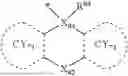


Sources:
- United States Patent and Trademark Office - verify current appl. status at the USPTO↗
Similar patent applications:
- » 20240324440
LIGHT-EMITTING DEVICE INCLUDING ORGANOMETALLIC COMPOUND, ELECTRONIC DEVICE INCLUDING LIGHT-EMITTING DEVICE, AND THE ORGANOMETALLIC COMPOUND - » 20240260449
LIGHT-EMITTING DEVICE INCLUDING ORGANOMETALLIC COMPOUND, ELECTRONIC APPARATUS INCLUDING LIGHT-EMITTING DEVICE, AND ORGANOMETALLIC COMPOUND - » 20240206320
LIGHT-EMITTING DEVICE INCLUDING ORGANOMETALLIC COMPOUND, ELECTRONIC DEVICE INCLUDING THE LIGHT-EMITTING DEVICE, AND THE ORGANOMETALLIC COMPOUND - » 20240180022
LIGHT-EMITTING DEVICE INCLUDING ORGANOMETALLIC COMPOUND, ELECTRONIC DEVICE INCLUDING THE LIGHT-EMITTING DEVICE, AND THE ORGANOMETALLIC COMPOUND - » 20230060808
LIGHT-EMITTING DEVICE INCLUDING ORGANOMETALLIC COMPOUND, ELECTRONIC APPARATUS INCLUDING THE LIGHT-EMITTING DEVICE, AND ORGANOMETALLIC COMPOUND - » 20240284782
LIGHT-EMITTING DEVICE INCLUDING ORGANOMETALLIC COMPOUND, ELECTRONIC APPARATUS INCLUDING THE LIGHT-EMITTING DEVICE, THE ORGANOMETALLIC COMPOUND - » 20220402956
LIGHT-EMITTING DEVICE INCLUDING ORGANOMETALLIC COMPOUND, ELECTRONIC APPARATUS INCLUDING THE LIGHT-EMITTING DEVICE, AND THE ORGANOMETALLIC COMPOUND - » 20230225189
LIGHT-EMITTING DEVICE INCLUDING ORGANOMETALLIC COMPOUND, ELECTRONIC APPARATUS INCLUDING THE LIGHT-EMITTING DEVICE, AND THE ORGANOMETALLIC COMPOUND - » 20220320446
LIGHT-EMITTING DEVICE INCLUDING ORGANOMETALLIC COMPOUND, ELECTRONIC APPARATUS INCLUDING THE LIGHT-EMITTING DEVICE, AND THE ORGANOMETALLIC COMPOUND - » 20230225190
LIGHT-EMITTING DEVICE INCLUDING ORGANOMETALLIC COMPOUND, ELECTRONIC APPARATUS INCLUDING THE LIGHT-EMITTING DEVICE, AND THE ORGANOMETALLIC COMPOUND
Recent applications in this class:
- » 20250171480 2025-05-29
ORGANIC ELECTROLUMINESCENT MATERIALS AND DEVICES - » 20250145649 2025-05-08
ORGANIC ELECTROLUMINESCENT MATERIALS AND DEVICES - » 20250136628 2025-05-01
ORGANIC ELECTROLUMINESCENT MATERIALS AND DEVICES - » 20250115632 2025-04-10
COMPOSITION, LIGHT-EMITTING DEVICE AND ELECTRONIC EQUIPMENT INCLUDING THE SAME, AND ORGANOMETALLIC COMPOUND - » 20250115631 2025-04-10
ORGANIC ELECTROLUMINESCENT MATERIALS AND DEVICES - » 20250066404 2025-02-27
ORGANOMETALLIC COMPOUND, ORGANIC LIGHT-EMITTING DEVICE INCLUDING THE SAME, AND ELECTRONIC APPARATUS INCLUDING THE ORGANIC LIGHT-EMITTING DEVICE - » 20250066403 2025-02-27
Linear boron-dipyrromethene electron donor having 180° coordination included angle and supramolecular metal macro-ring, and synthesis processes therefor and applications thereof - » 20250059223 2025-02-20
FUSED RING CARBAZOLE TETRADENTATE METAL PLATINUM (II) COMPLEX AND USE THEREOF - » 20250026775 2025-01-23
METAL PLATINUM (II) AND PALLADIUM (II) COMPLEX, ORGANIC LIGHT-EMITTING DEVICE AND DISPLAYING OR LIGHTING APPARATUS - » 20250019390 2025-01-16
ORGANIC ELECTROLUMINESCENT MATERIALS AND DEVICES
Recent applications for this Assignee:
- » 20250176402 2025-05-29
DISPLAY PANEL AND METHOD OF MANUFACTURING THE SAME - » 20250176397 2025-05-29
DISPLAY DEVICE - » 20250176395 2025-05-29
DISPLAY DEVICE - » 20250176381 2025-05-29
DISPLAY DEVICE AND METHOD OF MANUFACTURING THE SAME - » 20250176365 2025-05-29
DISPLAY DEVICE AND METHOD OF MANUFACTURING DISPLAY DEVICE - » 20250176364 2025-05-29
DISPLAY APPARATUS AND METHOD OF MANUFACTURING THE SAME - » 20250176359 2025-05-29
EMISSIVE DISPLAY DEVICE - » 20250176357 2025-05-29
DISPLAY DEVICE - » 20250176344 2025-05-29
DISPLAY PANEL, SMART GLASSES INCLUDING THE SAME, AND METHOD OF FABRICATING THE SAME - » 20250176265 2025-05-29
DISPLAY DEVICE AND THERMOSETTING CONDUCTIVE FILM