LIGHT-EMITTING DEVICE INCLUDING HETEROCYCLIC COMPOUND, ELECTRONIC APPARATUS INCLUDING THE LIGHT-EMITTING DEVICE, AND THE HETEROCYCLIC COMPOUND
US20250366367A1
2025-11-27
19/018,833
2025-01-13
Smart Summary: A new type of light-emitting device uses a special chemical called a heterocyclic compound. This device has two electrodes, one on each side, with a layer in between that contains the heterocyclic compound. The design allows it to produce light effectively. The light-emitting device can be used in various electronic gadgets, making them brighter and more efficient. Overall, this innovation enhances how devices emit light and can improve many electronic products. 🚀 TL;DR
Abstract:
Embodiments provide a heterocyclic compound, a light-emitting device including the heterocyclic compound, an electronic apparatus including the light-emitting device, and an electronic equipment including the light-emitting device. The light-emitting device includes a first electrode, a second electrode facing the first electrode, an interlayer between the first electrode and the second electrode, and the heterocyclic compound. The heterocyclic compound is represented by Formula 1, which is explained in the specification:
Inventors:
- Junha Park 131 🇰🇷 Yongin-si, South Korea
- Munki Sim 99 🇰🇷 Yongin-si, South Korea
- Minjung JUNG 80 🇰🇷 Yongin-si, South Korea
- MinJae SUNG 52 🇰🇷 Yongin-si, South Korea
- Chihyun RYOO 13 🇰🇷 Yongin-si, South Korea
- Hyungjong Kim 4 🇰🇷 Yongin-si, South Korea
- Taeil Kim 1 🇰🇷 Yongin-sip, South Korea
Assignee:
- SAMSUNG DISPLAY CO., LTD. 15,476 🇰🇷 Yongin-si, South Korea
Applicant:
Interested in similar patents?
Get notified when new applications in this technology area are published.
Classification:
C07F5/027 » CPC further
Compounds containing elements of Groups 3 or 13 of the Periodic System; Boron compounds Organoboranes and organoborohydrides
C09K11/02 » CPC further
Luminescent, e.g. electroluminescent, chemiluminescent materials Use of particular materials as binders, particle coatings or suspension media therefor
C09K11/06 » CPC further
Luminescent, e.g. electroluminescent, chemiluminescent materials containing organic luminescent materials
C09K2211/1007 » CPC further
Chemical nature of organic luminescent or tenebrescent compounds; Non-macromolecular compounds; Carbocyclic compounds Non-condensed systems
C09K2211/1018 » CPC further
Chemical nature of organic luminescent or tenebrescent compounds; Non-macromolecular compounds Heterocyclic compounds
C07F5/02 IPC
Compounds containing elements of Groups 3 or 13 of the Periodic System Boron compounds
Description
CROSS-REFERENCE TO RELATED APPLICATION(S)
This application claims priority to and benefits of Korean Patent Application No. 10-2024-0066592 under 35 U.S.C. § 119, filed on May 22, 2024, in the Korean Intellectual Property Office, the entire contents of which are incorporated herein by reference.
BACKGROUND
1. Technical Field
Embodiments relate to a light-emitting device including a heterocyclic compound, an electronic apparatus including the light-emitting device, an electronic equipment including the light-emitting device, and the heterocyclic compound.
2. Description of the Related Art
Light-emitting devices are self-emissive devices that have wide viewing angles, high contrast ratios, short response times, and excellent characteristics in terms of luminance, driving voltage, and response speed.
In a light-emitting device, a first electrode is arranged on a substrate, and a hole transport region, an emission layer, an electron transport region, and a second electrode are sequentially arranged on the first electrode. Holes provided from the first electrode move toward the emission layer through the hole transport region, and electrons provided from the second electrode move toward the emission layer through the electron transport region. Carriers, such as holes and electrons, recombine in the emission layer to produce excitons. The excitons may transition from an excited state to a ground state, thereby generating light.
It is to be understood that this background of the technology section is, in part, intended to provide useful background for understanding the technology. However, this background of the technology section may also include ideas, concepts, or recognitions that were not part of what was known or appreciated by those skilled in the pertinent art prior to a corresponding effective filing date of the subject matter disclosed herein.
SUMMARY
Embodiments include a light-emitting device including a heterocyclic compound, an electronic apparatus including the light-emitting device, an electronic apparatus including the light-emitting device, and the heterocyclic compound.
Additional aspects will be set forth in part in the description which follows and, in part, will be apparent from the description, or may be learned by practice of the embodiments.
According to embodiments, a light-emitting device may include
-
- a first electrode,
- a second electrode facing the first electrode,
- an interlayer between the first electrode and the second electrode and including an emission layer, and
- a heterocyclic compound represented by Formula 1:
In Formulae 1 to 3,
-
- X1 may be C(R6) or N,
- X2 may be C(R7) or N,
- X3 may be C(R8) or N,
- at least two of X1 to X3 may be N,
- ring CY1 to ring CY5 may each independently be a C4-C60 carbocyclic group or a C1-C60 heterocyclic group,
- Ar1 and Ar2 may each independently be a group represented by Formula 2, a C3-C60 carbocyclic group unsubstituted or substituted with at least one R10a, or a C1-C60 heterocyclic group unsubstituted or substituted with at least one R10a,
- at least one of Ar1 and Ar2 may each independently be a group represented by Formula 2,
- a1 to a5 may each independently be an integer from 0 to 20,
- b1 and b3 may each independently be an integer from 0 to 5,
- b2 may be an integer from 0 to 3,
- Z1 to Z3 and R1 to R10 may each independently be a group represented by Formula 3, hydrogen, deuterium, —F, —Cl, —Br, —I, a hydroxyl group, a cyano group, a nitro group, a C1-C60 alkyl group unsubstituted or substituted with at least one R10a, a C2-C60 alkenyl group unsubstituted or substituted with at least one R10a, a C2-C60 alkynyl group unsubstituted or substituted with at least one R10a, a C1-C60 alkoxy group unsubstituted or substituted with at least one R10a, a C3-C60 carbocyclic group unsubstituted or substituted with at least one R10a, a C1-C60 heterocyclic group unsubstituted or substituted with at least one R10a, —Si(Q1)(Q2)(Q3), —N(Q1)(Q2), —B(Q1)(Q2), —C(═O)(Q1), —S(═O)2(Q1), or —P(═O)(Q1)(Q2),
- at least one of R1 and R2 may each independently be a group represented by Formula 3,
- two or more adjacent groups among Z1 to Z3 and R1 to R10 may optionally be bonded to each other to form a C3-C60 carbocyclic group unsubstituted or substituted with at least one R10a or a C1-C60 heterocyclic group unsubstituted or substituted with at least one R10a,
- R10a may be:
- deuterium, —F, —Cl, —Br, —I, a hydroxyl group, a cyano group, or a nitro group;
- a C1-C60 alkyl group, a C2-C60 alkenyl group, a C2-C60 alkynyl group, or a C1-C60 alkoxy group, each unsubstituted or substituted with deuterium, —F, —Cl, —Br, —I, a hydroxyl group, a cyano group, a nitro group, a C3-C60 carbocyclic group, a C1-C60 heterocyclic group, a C6-C60 aryloxy group, a C6-C60 arylthio group, a C7-C60 arylalkyl group, a C2-C60 heteroarylalkyl group, —Si(Q11)(Q12)(Q13), —N(Q11)(Q12), —B(Q11)(Q12), —C(═O)(Q11), —S(═O)2(Q11), —P(═O)(Q11)(Q12), or any combination thereof;
- a C3-C60 carbocyclic group, a C1-C60 heterocyclic group, a C6-C60 aryloxy group, a C6-C60 arylthio group, a C7-C60 arylalkyl group, or a C2-C60 heteroarylalkyl group, each unsubstituted or substituted with deuterium, —F, —Cl, —Br, —I, a hydroxyl group, a cyano group, a nitro group, a C1-C60 alkyl group, a C2-C60 alkenyl group, a C2-C60 alkynyl group, a C1-C60 alkoxy group, a C3-C60 carbocyclic group, a C1-C60 heterocyclic group, a C6-C60 aryloxy group, a C6-C60 arylthio group, a C7-C60 arylalkyl group, a C2-C60 heteroarylalkyl group, —Si(Q21)(Q22)(Q23), —N(Q21)(Q22), —B(Q21)(Q22), —C(═O)(Q21), —S(═O)2(Q21), —P(═O)(Q21)(Q22), or any combination thereof; or
- —Si(Q31)(Q32)(Q33), —N(Q31)(Q32), —B(Q31)(Q32), —C(═O)(Q31), —S(═O)2(Q31), or —P(═O)(Q31)(Q32),
- Q1 to Q3, Q11 to Q13, Q21 to Q23, and Q31 to Q33 may each independently be:
- hydrogen, deuterium, —F, —Cl, —Br, —I, a hydroxyl group, a cyano group, or a nitro group, or
- a C1-C60 alkyl group, a C2-C60 alkenyl group, a C2-C60 alkynyl group, a C1-C60 alkoxy group, a C3-C60 carbocyclic group, a C1-C60 heterocyclic group, a C7-C60 arylalkyl group, or a C2-C60 heteroarylalkyl group, each unsubstituted or substituted with deuterium, —F, a cyano group, a C1-C60 alkyl group, a C1-C60 alkoxy group, a phenyl group, a biphenyl group, or any combination thereof, and
- * indicates a binding site to a neighboring atom.
In an embodiment, the interlayer may further include: a hole transport region between the first electrode and the emission layer; and an electron transport region between the emission layer and the second electrode,
-
- the hole transport region may include a hole injection layer, a hole transport layer, an emission auxiliary layer, an electron blocking layer, or any combination thereof, and
- the electron transport region may include a buffer layer, a hole-blocking layer, an electron control layer, an electron transport layer, an electron injection layer, or any combination thereof.
In an embodiment, the emission layer may include the heterocyclic compound.
In an embodiment, the emission layer may include a host and a dopant, and the dopant may include the heterocyclic compound.
In an embodiment, the emission layer may emit green light having a maximum emission wavelength in a range of about 510 nm to about 550 nm.
According to embodiments, an electronic apparatus may include the light-emitting device.
In an embodiment, the electronic apparatus may further include: a thin-film transistor electrically connected to the light-emitting device; and a color filter, a color conversion layer, a touch screen layer, a polarizing layer, or any combination thereof.
According to embodiments, an electronic equipment may include the light-emitting device.
In an embodiment, the electronic equipment may be a flat panel display, a curved display, a computer monitor, a medical monitor, a television, a billboard, an indoor light, an outdoor light, a signal light, a head-up display, a fully transparent display, a partially transparent display, a flexible display, a rollable display, a foldable display, a stretchable display, a laser printer, a telephone, a mobile phone, a tablet computer, a phablet, a personal digital assistant (PDA), a wearable device, a laptop computer, a digital camera, a camcorder, a viewfinder, a micro display, a three-dimensional (3D) display, a virtual reality display, an augmented reality display, a vehicle, a video wall with multiple displays tiled together, a theater screen, a stadium screen, a phototherapy device, or a signboard.
According to embodiments, a heterocyclic compound may be represented by Formula 1, which is explained herein.
In an embodiment, Ar1 and Ar2 may each independently be a group represented by Formula 2.
In an embodiment, ring CY1 to ring CY5 may each independently be a benzene group, a naphthalene group, an anthracene group, a phenanthrene group, a triphenylene group, a pyrene group, a chrysene group, an acenaphthylene group, a perylene group, a benzopyrene group, a benzochrysene group, a benzotriphenylene group, a fluoranthene group, a coronene group, a cyclopentadiene group, a 1,2,3,4-tetrahydronaphthalene group, an acridine group, a thiophene group, a furan group, an indole group, a benzoborole group, a benzophosphole group, an indene group, a benzosilole group, a benzogermole group, a benzothiophene group, a benzoselenophene group, a benzofuran group, a benzotellurophene group, a carbazole group, a dibenzoborole group, a dibenzophosphole group, a fluorene group, a dibenzosilole group, a dibenzogermole group, a dibenzothiophene group, a dibenzoselenorphene group, a dibenzofuran group, a dibenzotellurophene group, a dibenzothiophene 5-oxide group, a 9H-fluorene-9-one group, a dibenzothiophene 5,5-dioxide group, an azaindole group, an azabenzoborole group, an azabenzophosphole group, an azaindene group, an azabenzosilole group, an azabenzogermole group, an azabenzothiophene group, an azabenzoselenophene group, an azabenzofuran group, an azacarbazole group, an azadibenzoborole group, an azadibenzophosphole group, an azafluorene group, an azadibenzosilole group, an azadibenzogermole group, an azadibenzothiophene group, an azadibenzoselenophene group, an azadibenzofuran group, an azadibenzothiophene 5-oxide group, an aza-9H-fluoren-9-one group, an azadibenzothiophene 5,5-dioxide group, a pyridine group, a pyrimidine group, a pyrazine group, a pyridazine group, a triazine group, a quinoline group, an isoquinoline group, a quinoxaline group, a quinazoline group, a phenanthroline group, a pyrrole group, a pyrazole group, an imidazole group, a triazole group, an oxazole group, an isoxazole group, a thiazole group, an isothiazole group, an oxadiazole group, a thiadiazole group, a benzopyrazole group, a benzimidazole group, a benzoxazole group, a benzothiazole group, a benzoxadiazole group, a benzothiadiazole group, a 5,6,7,8-tetrahydroisoquinoline group, a 5,6,7,8-tetrahydroquinoline group, or indolo[3,2,1-jk]carbazole.
In an embodiment, ring CY4 and ring CY5 may each independently be a 6-membered ring.
In an embodiment, ring CY4 and ring CY5 may each independently be a benzene group, a naphthalene group, or a pyridine group.
In an embodiment, in Formula 1, a moiety represented by
may be a moiety represented by one of Formulae 4-1 to 4-9, which are explained below.
In an embodiment, Z1 to Z3 and R1 to R10 may each independently be:
-
- a group represented by Formula 3;
- deuterium, —F, —Cl, —Br, —I, a cyano group, a C1-C20 alkyl group, a C1-C20 alkoxy group, or a C1-C20 alkylthio group;
- a C1-C20 alkyl group, a C1-C20 alkoxy group, or a C1-C20 alkylthio group, each substituted with deuterium, —F, —Cl, —Br, —I, —CD3, —CD2H, —CDH2, —CF3, —CF2H, —CFH2, a cyano group, a C1-C10 alkyl group, a cyclopentyl group, a cyclohexyl group, a cycloheptyl group, a cyclopentenyl group, a cyclohexenyl group, a cycloheptenyl group, a phenyl group, a biphenyl group, a naphthyl group, a pyridinyl group, a pyrimidinyl group, or any combination thereof;
- a cyclopentyl group, a cyclohexyl group, a cycloheptyl group, a cyclopentenyl group, a cyclohexenyl group, a cycloheptenyl group, a phenyl group, a biphenyl group, a C1-C10 alkylphenyl group, a naphthyl group, a fluorenyl group, a phenanthrenyl group, an anthracenyl group, a pyrenyl group a pyrrolyl group, a thiophenyl group, a furanyl group, an imidazolyl group, a pyrazolyl group, a thiazolyl group, an isothiazolyl group, an oxazolyl group, an isoxazolyl group, a pyridinyl group, a pyrazinyl group, a pyrimidinyl group, a pyridazinyl group, an isoindolyl group, an indolyl group, an indazolyl group, a purinyl group, a quinolinyl group, an isoquinolinyl group, a benzoquinolinyl group, a quinoxalinyl group, a quinazolinyl group, a cinnolinyl group, a phthalazinyl group, a carbazolyl group, a phenanthrolinyl group, a benzimidazolyl group, a benzofuranyl group, a benzothiophenyl group, a benzoisothiazolyl group, a benzoxazolyl group, a benzoisoxazolyl group, a triazolyl group, a tetrazolyl group, an oxadiazolyl group, a triazinyl group, a dibenzofuranyl group, a dibenzothiophenyl group, a benzocarbazolyl group, a dibenzocarbazolyl group, an imidazopyridinyl group, an imidazopyrimidinyl group, an azacarbazolyl group, an azadibenzofuranyl group, an azadibenzothiophenyl group, an azafluorenyl group, or an azadibenzosilolyl group, each unsubstituted or substituted with deuterium, —F, —Cl, —Br, —I, —CD3, —CD2H, —CDH2, —CF3, —CF2H, —CFH2, a cyano group, a C1-C20 alkyl group, a C1-C20 alkoxy group, a C1-C20 alkylthio group, a cyclopentyl group, a cyclohexyl group, a cycloheptyl group, a cyclopentenyl group, a cyclohexenyl group, a cycloheptenyl group, a phenyl group, a biphenyl group, a C1-C10 alkylphenyl group, a naphthyl group, a fluorenyl group, a phenanthrenyl group, an anthracenyl group, a pyrenyl group, a pyrrolyl group, a thiophenyl group, a furanyl group, an imidazolyl group, a pyrazolyl group, a thiazolyl group, an isothiazolyl group, an oxazolyl group, an isoxazolyl group, a pyridinyl group, a pyrazinyl group, a pyrimidinyl group, a pyridazinyl group, an isoindolyl group, an indolyl group, an indazolyl group, a purinyl group, a quinolinyl group, an isoquinolinyl group, a benzoquinolinyl group, a quinoxalinyl group, a quinazolinyl group, a cinnolinyl group, a phthalazinyl group, a carbazolyl group, a phenanthrolinyl group, a benzimidazolyl group, a benzofuranyl group, a benzothiophenyl group, a benzothiazolyl group, a benzoisoxazolyl group, a triazolyl group, a tetrazolyl group, an oxadiazolyl group, a triazinyl group, a dibenzofuranyl group, a dibenzothiophenyl group, a benzocarbazolyl group, a dibenzocarbazolyl group, an imidazopyridinyl group, an imidazopyrimidinyl group, —O(Q31), —S(Q31), —Si(Q31)(Q32)(Q33), —N(Q31)(Q32), —P(═O)(Q1)(Q2), or any combination thereof; or
- —C(Q1)(Q2)(Q3), —Si(Q1)(Q2)(Q3), —N(Q1)(Q2), or —P(═O)(Q1)(Q2), and
- Q1 to Q3 and Q31 to Q33 may each independently be: hydrogen; deuterium; —F; —Cl; —Br; —I; a cyano group; a C1-C60 alkyl group; a C2-C60 alkenyl group; a C2-C60 alkynyl group; a C1-C60 alkoxy group; a C1-C60 alkylthio group; or a C3-C60 carbocyclic group or a C1-C60 heterocyclic group, each unsubstituted or substituted with deuterium, —F, a cyano group, a C1-C60 alkyl group, a C1-C60 alkoxy group, a C1-C60 alkylthio group, a phenyl group, a biphenyl group, or any combination thereof.
In an embodiment, the heterocyclic compound may be represented by Formula 1A or Formula 1B, which are explained below.
In an embodiment, the heterocyclic compound may be represented by one of Formulae 1-1 to 1-4, which are explained below.
In an embodiment, in Formula 1-1, at least one of R12 and R22 may each independently be a group represented by Formula 3; and in Formulae 1-2 to 1-4, R12 may be a group represented by Formula 3.
In an embodiment, the heterocyclic compound may be one of Compounds 1 to 60, which are explained below.
It is to be understood that the embodiments above are described in a generic and explanatory sense only and not for the purpose of limitation, and the disclosure is not limited to the embodiments described above.
BRIEF DESCRIPTION OF THE DRAWINGS
The accompanying drawings are included to provide a further understanding of the embodiments, and are incorporated in and constitute a part of this specification.
The drawings illustrate embodiments of the disclosure and principles thereof. The above and other aspects and features of the disclosure will become more apparent by describing in detail embodiments thereof with the reference to the accompanying drawings, in which:
FIG. 1 is a schematic cross-sectional view of a light-emitting device according to an embodiment;
FIG. 2 is a schematic cross-sectional view of an electronic apparatus according to an embodiment;
FIG. 3 is a schematic cross-sectional view of an electronic apparatus according to another embodiment;
FIG. 4 is a schematic perspective view of an electronic equipment including a light-emitting device according to an embodiment;
FIG. 5 is a schematic perspective view of an exterior of a vehicle as an electronic equipment including a light-emitting device according to an embodiment; and
FIGS. 6A to 6C are each a schematic diagram of an interior of a vehicle according to embodiments.
DETAILED DESCRIPTION OF THE EMBODIMENTS
The disclosure will now be described more fully hereinafter with reference to the accompanying drawings, in which embodiments are shown. This disclosure may, however, be embodied in different forms and should not be construed as limited to the embodiments set forth herein. Rather, these embodiments are provided so that this disclosure will be thorough and complete, and will fully convey the scope of the disclosure to those skilled in the art.
In the drawings, the sizes, thicknesses, ratios, and dimensions of the elements may be exaggerated for ease of description and for clarity. Like reference numbers and reference characters refer to like elements throughout.
In the specification, it will be understood that when an element (or region, layer, part, etc.) is referred to as being “on”, “connected to”, or “coupled to” another element, it can be directly on, connected to, or coupled to the other element, or one or more intervening elements may be present therebetween. In a similar sense, when an element (or region, layer, part, etc.) is described as “covering” another element, it can directly cover the other element, or one or more intervening elements may be present therebetween.
In the specification, when an element is “directly on”, “directly connected to”, or “directly coupled to” another element, there are no intervening elements present. For example, “directly on” may mean that two layers or two elements are disposed without an additional element such as an adhesion element therebetween.
In the specification, the expressions used in the singular such as “a”, “an”, and “the” are intended to include the plural forms as well, unless the context clearly indicates otherwise.
In the specification, the term “and/or” includes any and all combinations of one or more of the associated listed items. For example, “A and/or B” may be understood to mean “A, B, or A and B”. The terms “and” and “or” may be used in the conjunctive or disjunctive sense and may be understood to be equivalent to “and/or”.
In the specification and the claims, the term “at least one of” is intended to include the meaning of “at least one selected from the group consisting of” for the purpose of its meaning and interpretation. For example, “at least one of A, B, and C” may be understood to mean A only, B only, C only, or any combination of two or more of A, B, and C, such as ABC, ACC, BC, or CC. When preceding a list of elements, the term, “at least one of”, modifies the entire list of elements and does not modify the individual elements of the list.
It will be understood that, although the terms first, second, etc. may be used herein to describe various elements, these elements should not be limited by these terms. These terms are only used to distinguish one element from another element.
Thus, a first element could be termed a second element without departing from the teachings of the disclosure. Similarly, a second element could be termed a first element, without departing from the scope of the disclosure.
The spatially relative terms “below”, “beneath”, “lower”, “above”, “upper”, or the like, may be used herein for ease of description to describe the relations between one element or component and another element or component as illustrated in the drawings. It will be understood that the spatially relative terms are intended to encompass different orientations of the device in use or operation, in addition to the orientation depicted in the drawings. For example, in the case where a device illustrated in the drawing is turned over, the device positioned “below” or “beneath” another device may be placed “above” another device. Accordingly, the illustrative term “below” may include both the lower and upper positions. The device may also be oriented in other directions and thus the spatially relative terms may be interpreted differently depending on the orientations.
The terms “about” or “approximately” as used herein is inclusive of the stated value and means within an acceptable range of deviation for the recited value as determined by one of ordinary skill in the art, considering the measurement in question and the error associated with measurement of the recited quantity (i.e., the limitations of the measurement system). For example, “about” may mean within one or more standard deviations, or within ±20%, ±10%, or ±5% of the stated value.
It should be understood that the terms “comprises”, “comprising”, “includes”, “including”, “have”, “having”, “contains”, “containing”, and the like are intended to specify the presence of stated features, integers, steps, operations, elements, components, or combinations thereof in the disclosure, but do not preclude the presence or addition of one or more other features, integers, steps, operations, elements, components, or combinations thereof.
Unless otherwise defined or implied herein, all terms (including technical and scientific terms) used have the same meaning as commonly understood by those skilled in the art to which this disclosure pertains. It will be further understood that terms, such as those defined in commonly used dictionaries, should be interpreted as having a meaning that is consistent with their meaning in the context of the relevant art and should not be interpreted in an ideal or excessively formal sense unless clearly defined in the specification.
According to embodiments, a light-emitting device (e.g., an organic light-emitting device) may include:
-
- a first electrode;
- a second electrode facing the first electrode;
- an interlayer between the first electrode and the second electrode and including an emission layer; and
- a heterocyclic compound represented by Formula 1.
Further details on a heterocyclic compound represented by Formula 1 are provided below:
In Formulae 1 to 3,
-
- X1 may be C(R6) or N,
- X2 may be C(R7) or N,
- X3 may be C(R8) or N,
- at least two of X1 to X3 may be N,
- ring CY1 to ring CY5 may each independently be a C4-C60 carbocyclic group or a C1-C60 heterocyclic group,
- Ar1 and Ar2 may each independently be a group represented by Formula 2, a C3-C60 carbocyclic group unsubstituted or substituted with at least one R10a, or a C1-C60 heterocyclic group unsubstituted or substituted with at least one R10a,
- at least one of Ar1 and Ar2 may each independently be a group represented by Formula 2,
- a1 to a5 may each independently be an integer from 0 to 20,
- b1 and b3 may each independently be an integer from 0 to 5,
- b2 may be an integer from 0 to 3,
- Z1 to Z3 and R1 to R10 may each independently be a group represented by Formula 3, hydrogen, deuterium, —F, —Cl, —Br, —I, a hydroxyl group, a cyano group, a nitro group, a C1-C60 alkyl group unsubstituted or substituted with at least one R10a, a C2-C60 alkenyl group unsubstituted or substituted with at least one R10a, a C2-C60 alkynyl group unsubstituted or substituted with at least one R10a, a C1-C60 alkoxy group unsubstituted or substituted with at least one R10a, a C3-C60 carbocyclic group unsubstituted or substituted with at least one R10a, a C1-C60 heterocyclic group unsubstituted or substituted with at least one R10a, —Si(Q1)(Q2)(Q3), —N(Q1)(Q2), —B(Q1)(Q2), —C(═O)(Q1), —S(═O)2(Q1), or —P(═O)(Q1)(Q2),
- at least one of R1 and R2 may each independently be a group represented by Formula 3,
- two or more adjacent groups among Z1 to Z3 and R1 to R10 may optionally be bonded to each other to form a C3-C60 carbocyclic group unsubstituted or substituted with at least one R10a or a C1-C60 heterocyclic group unsubstituted or substituted with at least one R10a,
- R10a may be:
- deuterium, —F, —Cl, —Br, —I, a hydroxyl group, a cyano group, or a nitro group;
- a C1-C60 alkyl group, a C2-C60 alkenyl group, a C2-C60 alkynyl group, or a C1-C60 alkoxy group, each unsubstituted or substituted with deuterium, —F, —Cl, —Br, —I, a hydroxyl group, a cyano group, a nitro group, a C3-C60 carbocyclic group, a C1-C60 heterocyclic group, a C6-C60 aryloxy group, a C6-C60 arylthio group, a C7-C60 arylalkyl group, a C2-C60 heteroarylalkyl group, —Si(Q11)(Q12)(Q13), —N(Q11)(Q12), —B(Q11)(Q12), —C(═O)(Q11), —S(═O)2(Q11), —P(═O)(Q11)(Q12), or any combination thereof;
- a C3-C60 carbocyclic group, a C1-C60 heterocyclic group, a C6-C60 aryloxy group, a C6-C60 arylthio group, a C7-C60 arylalkyl group, or a C2-C60 heteroarylalkyl group, each unsubstituted or substituted with deuterium, —F, —Cl, —Br, —I, a hydroxyl group, a cyano group, a nitro group, a C1-C60 alkyl group, a C2-C60 alkenyl group, a C2-C60 alkynyl group, a C1-C60 alkoxy group, a C3-C60 carbocyclic group, a C1-C60 heterocyclic group, a C6-C60 aryloxy group, a C6-C60 arylthio group, a C7-C60 arylalkyl group, a C2-C60 heteroarylalkyl group, —Si(Q21)(Q22)(Q23), —N(Q21)(Q22), —B(Q21)(Q22), —C(═O)(Q21), —S(═O)2(Q21), —P(═O)(Q21)(Q22), or any combination thereof; or
- —Si(Q31)(Q32)(Q33), —N(Q31)(Q32), —B(Q31)(Q32), —C(═O)(Q31), —S(═O)2(Q31), or —P(═O)(Q31)(Q32),
- Q1 to Q3, Q11 to Q13, Q21 to Q23, and Q31 to Q33 may each independently be:
- hydrogen, deuterium, —F, —Cl, —Br, —I, a hydroxyl group, a cyano group, or a nitro group; or
- a C1-C60 alkyl group, a C2-C60 alkenyl group, a C2-C60 alkynyl group, a C1-C60 alkoxy group, a C3-C60 carbocyclic group, a C1-C60 heterocyclic group, a C7-C60 arylalkyl group, or a C2-C60 heteroarylalkyl group, each unsubstituted or substituted with deuterium, —F, a cyano group, a C1-C60 alkyl group, a C1-C60 alkoxy group, a phenyl group, a biphenyl group, or any combination thereof, and
- * indicates a binding site to a neighboring atom.
In an embodiment, Ar1 and Ar2 may each independently be a group represented by Formula 2.
In an embodiment, ring CY1 to ring CY5 may each independently be a benzene group, a naphthalene group, an anthracene group, a phenanthrene group, a triphenylene group, a pyrene group, a chrysene group, an acenaphthylene group, a perylene group, a benzopyrene group, a benzochrysene group, a benzotriphenylene group, a fluoranthene group, a coronene group, a cyclopentadiene group, a 1,2,3,4-tetrahydronaphthalene group, an acridine group, a thiophene group, a furan group, an indole group, a benzoborole group, a benzophosphole group, an indene group, a benzosilole group, a benzogermole group, a benzothiophene group, a benzoselenophene group, a benzofuran group, a benzotellurophene group, a carbazole group, a dibenzoborole group, a dibenzophosphole group, a fluorene group, a dibenzosilole group, a dibenzogermole group, a dibenzothiophene group, a dibenzoselenorphene group, a dibenzofuran group, a dibenzotellurophene group, a dibenzothiophene 5-oxide group, a 9H-fluorene-9-one group, a dibenzothiophene 5,5-dioxide group, an azaindole group, an azabenzoborole group, an azabenzophosphole group, an azaindene group, an azabenzosilole group, an azabenzogermole group, an azabenzothiophene group, an azabenzoselenophene group, an azabenzofuran group, an azacarbazole group, an azadibenzoborole group, an azadibenzophosphole group, an azafluorene group, an azadibenzosilole group, an azadibenzogermole group, an azadibenzothiophene group, an azadibenzoselenophene group, an azadibenzofuran group, an azadibenzothiophene 5-oxide group, an aza-9H-fluoren-9-one group, an azadibenzothiophene 5,5-dioxide group, a pyridine group, a pyrimidine group, a pyrazine group, a pyridazine group, a triazine group, a quinoline group, an isoquinoline group, a quinoxaline group, a quinazoline group, a phenanthroline group, a pyrrole group, a pyrazole group, an imidazole group, a triazole group, an oxazole group, an isoxazole group, a thiazole group, an isothiazole group, an oxadiazole group, a thiadiazole group, a benzopyrazole group, a benzimidazole group, a benzoxazole group, a benzothiazole group, a benzoxadiazole group, a benzothiadiazole group, a 5,6,7,8-tetrahydroisoquinoline group, a 5,6,7,8-tetrahydroquinoline group, or indolo[3,2,1-jk]carbazole.
For example, ring CY1 to ring CY5 may each independently be a benzene group, a carbazole group, a fluorene group, a dibenzothiophene group, a dibenzofuran group, or indolo[3,2,1-jk]carbazole.
In an embodiment, ring CY1 to ring CY5 may each independently be a 6-membered ring.
In an embodiment, in Formula 1, two or more adjacent groups among R1 to R3 may optionally be bonded to each other to form a C3-C60 carbocyclic group unsubstituted or substituted with at least one R10a or a C1-C60 heterocyclic group unsubstituted or substituted with at least one R10a. For example, when a1 is 2 or more, two or more of R1 may be bonded to each other to form a carbazole group, a fluorene group, dibenzothiophene, dibenzofuran, or indolo[3,2,1-jk]carbazole, each unsubstituted or substituted with at least one R10a, and when a2 is 2 or more, two or more of R2 may optionally be bonded to each other to form a carbazole group, a fluorene group, dibenzothiophene, dibenzofuran, or indolo[3,2,1-jk]carbazole, each unsubstituted or substituted with at least one R10a. Examples in which multiple R1 groups or multiple R2 groups are bonded to each other to form a C3-C60 carbocyclic group unsubstituted or substituted with at least one R10a, a C1-C60 heterocyclic group unsubstituted or substituted with at least one R10a may include Compounds 30 and 33 to 35.
In an embodiment, in Formula 3, ring CY4 and ring CY5 may each independently be a 6-membered ring.
In an embodiment, in Formula 3, ring CY4 and ring CY5 may each independently be a benzene group, a naphthalene group, or a pyridine group.
In an embodiment, in Formula 1, a moiety represented by
may be a moiety represented by any one of Formulae 4-1 to 4-9:
In Formulae 4-1 to 4-9,
-
- Y1 may be O or S,
- c2 may be an integer from 0 to 2,
- c4 may be an integer from 0 to 4, and
- c8 may be an integer from 0 to 8,
- R7 to R10 and R10a may be the same as defined in Formula 1, and
- * indicates a binding site to a neighboring atom.
In an embodiment, Z1 to Z3 and R1 to R10 may each independently be:
-
- a group represented by Formula 3;
- deuterium, —F, —Cl, —Br, —I, a cyano group, a C1-C20 alkyl group, a C1-C20 alkoxy group, or a C1-C20 alkylthio group;
- a C1-C20 alkyl group, a C1-C20 alkoxy group, or a C1-C20 alkylthio group, each substituted with deuterium, —F, —Cl, —Br, —I, —CDs, —CD2H, —CDH2, —CF3, —CF2H, —CFH2, a cyano group, a C1-C10 alkyl group, a cyclopentyl group, a cyclohexyl group, a cycloheptyl group, a cyclopentenyl group, a cyclohexenyl group, a cycloheptenyl group, a phenyl group, a biphenyl group, a naphthyl group, a pyridinyl group, a pyrimidinyl group, or any combination thereof;
- a cyclopentyl group, a cyclohexyl group, a cycloheptyl group, a cyclopentenyl group, a cyclohexenyl group, a cycloheptenyl group, a phenyl group, a biphenyl group, a C1-C10 alkylphenyl group, a naphthyl group, a fluorenyl group, a phenanthrenyl group, an anthracenyl group, a pyrenyl group a pyrrolyl group, a thiophenyl group, a furanyl group, an imidazolyl group, a pyrazolyl group, a thiazolyl group, an isothiazolyl group, an oxazolyl group, an isoxazolyl group, a pyridinyl group, a pyrazinyl group, a pyrimidinyl group, a pyridazinyl group, an isoindolyl group, an indolyl group, an indazolyl group, a purinyl group, a quinolinyl group, an isoquinolinyl group, a benzoquinolinyl group, a quinoxalinyl group, a quinazolinyl group, a cinnolinyl group, a phthalazinyl group, a carbazolyl group, a phenanthrolinyl group, a benzimidazolyl group, a benzofuranyl group, a benzothiophenyl group, a benzoisothiazolyl group, a benzoxazolyl group, a benzoisoxazolyl group, a triazolyl group, a tetrazolyl group, an oxadiazolyl group, a triazinyl group, a dibenzofuranyl group, a dibenzothiophenyl group, a benzocarbazolyl group, a dibenzocarbazolyl group, an imidazopyridinyl group, an imidazopyrimidinyl group, an azacarbazolyl group, an azadibenzofuranyl group, an azadibenzothiophenyl group, an azafluorenyl group, or an azadibenzosilolyl group, each unsubstituted or substituted with deuterium, —F, —Cl, —Br, —I, —CDs, —CD2H, —CDH2, —CF3, —CF2H, —CFH2, a cyano group, a C1-C20 alkyl group, a C1-C20 alkoxy group, a C1-C20 alkylthio group, a cyclopentyl group, a cyclohexyl group, a cycloheptyl group, a cyclopentenyl group, a cyclohexenyl group, a cycloheptenyl group, a phenyl group, a biphenyl group, a C1-C10 alkylphenyl group, a naphthyl group, a fluorenyl group, a phenanthrenyl group, an anthracenyl group, a pyrenyl group, a pyrrolyl group, a thiophenyl group, a furanyl group, an imidazolyl group, a pyrazolyl group, a thiazolyl group, an isothiazolyl group, an oxazolyl group, an isoxazolyl group, a pyridinyl group, a pyrazinyl group, a pyrimidinyl group, a pyridazinyl group, an isoindolyl group, an indolyl group, an indazolyl group, a purinyl group, a quinolinyl group, an isoquinolinyl group, a benzoquinolinyl group, a quinoxalinyl group, a quinazolinyl group, a cinnolinyl group, a phthalazinyl group, a carbazolyl group, a phenanthrolinyl group, a benzimidazolyl group, a benzofuranyl group, a benzothiophenyl group, a benzothiazolyl group, a benzoisoxazolyl group, a triazolyl group, a tetrazolyl group, an oxadiazolyl group, a triazinyl group, a dibenzofuranyl group, a dibenzothiophenyl group, a benzocarbazolyl group, a dibenzocarbazolyl group, an imidazopyridinyl group, an imidazopyrimidinyl group, —O(Q31), —S(Q31), —Si(Q31)(Q32)(Q33), —N(Q31)(Q32), —P(═O)(Q1)(Q2), or any combination thereof; or
- —C(Q1)(Q2)(Q3), —Si(Q1)(Q2)(Q3), —N(Q1)(Q2), or —P(═O)(Q1)(Q2), and
- Q1 to Q3 and Q31 to Q33 may each independently be: hydrogen; deuterium; —F; —Cl; —Br; —I; a cyano group; a C1-C60 alkyl group; a C2-C60 alkenyl group; a C2-C60 alkynyl group; a C1-C60 alkoxy group; a C1-C60 alkylthio group; or a C3-C60 carbocyclic group or a C1-C60 heterocyclic group, each unsubstituted or substituted with deuterium, —F, a cyano group, a C1-C60 alkyl group, a C1-C60 alkoxy group, a C1-C60 alkylthio group, a phenyl group, a biphenyl group, or any combination thereof.
In an embodiment, at least one of Z1 to Z3 in Formula 2 may be a tert-butyl group.
In an embodiment, the heterocyclic compound may be represented by Formula 1A or Formula 1B:
In Formulae 1A and 1B,
-
- R31 to R33 may each independently be the same as defined in connection with R3 in Formula 1, and
- X1 to X3, ring CY1, ring CY2, Ar1, Ar2, R1, R2, R9, R10, a1, and a2 may each be the same as defined in Formula 1.
In an embodiment, the heterocyclic compound may be represented by one of Formulae 1-1 to 1-4:
-
- In Formulae 1-1 to 1-4,
- Y2 may be O, S, N(R10b), or C(R10b)(R10c),
- d4 may be an integer from 0 to 4,
- d7 may be an integer from 0 to 7,
- R11 to R14 may each independently be the same as defined in connection with R1 in Formula 1,
- R21 to R24 may each independently be the same as defined in connection with R2 in Formula 1,
- R10b and R10c may each independently be the same as defined in connection with R10a in Formula 1, and
- X1 to X3, ring CY3, Ar1, Ar2, R3, R9, R10, R10a, and a3 may each be the same as defined in Formula 1.
In an embodiment, in Formula 1-1, at least one of R12 and R22 may each independently be a group represented by Formula 3.
In an embodiment, in Formulae 1-2 to 1-4, R12 may be a group represented by Formula 3.
In an embodiment, a heterocyclic compound represented by Formula 1 may include at least one deuterium.
In an embodiment, the heterocyclic compound may be any one of Compounds 1 to 60:
Although not limited by any particular theory, when a device including a heterocyclic compound is manufactured to emit light in a green wavelength range, if the heterocyclic compound emits blue light (for example, a heterocyclic compound represented by Formula 1 that includes a moiety represented by
wherein the moiety is a pyridine moiety), the target emission wavelength range cannot be achieved, which leads to lowered efficiency and lifespan. However, when a device including the heterocyclic compound is manufactured to emit light in a green wavelength range, the efficiency and lifespan may be improved by including a heterocyclic compound represented by Formula 1 in which at least two of X1 to X3 are N, so that it emits green light.
Although not limited by any particular theory, when at least one of Ar1 and Ar2 in Formula 1 is each independently a group represented by Formula 2, the steric effect caused by such a structure may reduce intermolecular interactions, may increase the stability of the material, and may suppress Dexter energy transfer, thereby resulting in significant improvement in lifespan when applied to a device. As the bulkiness of a terphenyl group represented by Formula 2 renders molecules more rigid, the FWHM may be narrow, and the Stokes-shift may be reduced when manufactured as a film.
Although not limited by any particular theory, when at least one of R1 and R2 in Formula 1 is each independently a group represented by Formula 3, the heterocyclic compound may have a deep HOMO energy level, which prevents direct recombination that would be caused at a shallow HOMO energy level. Accordingly, when the heterocyclic compound is applied to a device, the device lifespan may be improved significantly.
Therefore, when the heterocyclic compound is applied to a light-emitting device, the driving voltage may be lowered, and the color purity, luminescence efficiency, and lifespan characteristics may be improved. For example, due to the inclusion of the heterocyclic compound in the emission layer, a green light-emitting device having low driving voltage, high color purity, high luminescence efficiency, and long lifespan may be implemented.
The heterocyclic compound may emit green light. For example, the heterocyclic compound may emit green light with a maximum emission wavelength in a range of about 500 nm to about 570 nm. For example, the heterocyclic compound may emit green light with a maximum emission wavelength in a range of about 510 nm to about 550 nm. However, the disclosure is not limited thereto. Thus, the heterocyclic compound may be useful for the manufacture of a light-emitting device emitting green light.
In an embodiment, the heterocyclic compound may emit green light having a maximum emission wavelength in a range of about 510 nm to about 550 nm.
In an embodiment, the Stokes-shift of the heterocyclic compound may be equal to or less than about 20 nm.
In embodiments, the heterocyclic compound may have a top emission CIEx coordinate in a range of about 0.250 to about 0.280. For example, the heterocyclic compound may have a top emission CIEx coordinate in a range of about 0.260 to about 0.275. For example, the heterocyclic compound may have a top emission CIEx coordinate in a range of about 0.265 to about 0.270. In embodiments, the heterocyclic compound may have a top emission CIEy coordinate in a range of about 0.650 to about 0.750. For example, the heterocyclic compound may have a top emission CIEy coordinate in a range of about 0.680 to about 0.730. For example, the heterocyclic compound may have a top emission CIEy coordinate in a range of about 0.690 to about 0.710.
Synthesis methods of the heterocyclic compound may be recognizable by one of ordinary skill in the art by referring to the Examples provided below.
In an embodiment, the first electrode of the light-emitting device may be an anode,
-
- the second electrode of the light-emitting device may be a cathode,
- the interlayer may further include a hole transport region between the first electrode and the emission layer, and an electron transport region between the emission layer and the second electrode,
- the hole transport region may include a hole injection layer, a hole transport layer, an emission auxiliary layer, an electron blocking layer, or any combination thereof, and
- the electron transport region may include a hole blocking layer, an electron transport layer, an electron injection layer, or any combination thereof.
In an embodiment, the emission layer may include the heterocyclic compound.
For example, the emission layer may emit green light having a maximum emission wavelength in a range of about 500 nm to about 570 nm.
In embodiments, the emission layer of the light-emitting device may include a dopant and a host, and the dopant may include the heterocyclic compound. For example, the heterocyclic compound may serve as a dopant. The emission layer may emit, for example, green light. The green light may have a maximum emission wavelength in a range of, for example, about 500 nm to about 570 nm.
In an embodiment, the emission layer may emit green light having a maximum emission wavelength in a range of about 510 nm to about 550 nm.
In an embodiment, the emission layer may include a host and a dopant.
In an embodiment, in the emission layer, an amount of the host may be greater than an amount of the dopant, based on weight.
In an embodiment, the host may be a host as described below.
Therefore, a light-emitting device (for example, an organic light-emitting device) including the heterocyclic compound as described above may have high luminescence efficiency, low driving voltage, and long lifespan characteristics.
In the specification, the term “interlayer” may refer to a single layer and/or all layers between a first electrode and a second electrode of the light-emitting device.
According to an embodiment, an electronic apparatus may include the light-emitting device. The electronic apparatus may further include a thin-film transistor. In an embodiment, the electronic apparatus may further include a thin-film transistor including a source electrode and a drain electrode, wherein the first electrode of the light-emitting device may be electrically connected to the source electrode or the drain electrode. In an embodiment, the electronic apparatus may further include a color filter, a color conversion layer, a touch screen layer, a polarizing layer, or any combination thereof. Further details on the electronic apparatus may be the same as described herein.
According to an embodiment, an electronic equipment may include the light-emitting device.
For example, the electronic equipment may be a flat panel display, a curved display, a computer monitor, a medical monitor, a TV, a billboard, an indoor light, an outdoor light, a signal light, a head-up display, a fully transparent display, a partially transparent display, a flexible display, a rollable display, a foldable display, a stretchable display, a laser printer, a telephone, a mobile phone, a tablet computer, a phablet, a personal digital assistant (PDA), a wearable device, a laptop computer, a digital camera, a camcorder, a viewfinder, a micro display, a three-dimensional (3D) display, a virtual reality display, an augmented reality display, a vehicle, a video wall with multiple displays tiled together, a theater screen, a stadium screen, a phototherapy device, or a signboard.
Description of FIG. 1
FIG. 1 is a schematic cross-sectional view of a light-emitting device 10 according to an embodiment. The light-emitting device 10 includes a first electrode 110, an interlayer 130, and a second electrode 150.
Hereinafter, a structure of the light-emitting device 10 according to an embodiment and a method of manufacturing the light-emitting device 10 are described with reference to FIG. 1.
[First Electrode 110]
In FIG. 1, a substrate may be further included under the first electrode 110 or on the second electrode 150. The substrate may be a glass substrate or a plastic substrate. In an embodiment, the substrate may be a flexible substrate and may include plastics with excellent heat resistance and durability, such as polyimide, polyethylene terephthalate (PET), polycarbonate, polyethylene naphthalate, polyarylate (PAR), polyetherimide, or any combination thereof.
The first electrode 110 may be formed by, for example, depositing or sputtering a material for forming the first electrode 110 on the substrate. When the first electrode 110 is an anode, a material for forming the first electrode 110 may be a high-work function material that facilitates injection of holes.
The first electrode 110 may be a reflective electrode, a transflective electrode, or a transmissive electrode. When the first electrode 110 is a transmissive electrode, a material for forming the first electrode 110 may include indium tin oxide (ITO), indium zinc oxide (IZO), tin oxide (SnO2), zinc oxide (ZnO), or any combination thereof. In an embodiment, when the first electrode 110 is a transflective electrode or a reflective electrode, a material for forming the first electrode 110 may include magnesium (Mg), silver (Ag), aluminum (Al), aluminum-lithium (Al—Li), calcium (Ca), magnesium-indium (Mg—In), magnesium-silver (Mg—Ag), or any combination thereof.
The first electrode 110 may have a single-layer structure consisting of a single layer or a multilayer structure including multiple layers. In an embodiment, the first electrode 110 may have a three-layered structure of ITO/Ag/ITO.
[Interlayer 130]
The interlayer 130 may be disposed on the first electrode 110. The interlayer 130 includes an emission layer.
The interlayer 130 may further include a hole transport region arranged between the first electrode 110 and the emission layer, and an electron transport region arranged between the emission layer and the second electrode 150.
The interlayer 130 may further include, in addition to various organic materials, a metal-containing compound such as a heterocyclic compound, an inorganic material such as a quantum dot, and the like.
In an embodiment, the interlayer 130 may include, two or more emitting units sequentially stacked between the first electrode 110 and the second electrode 150, and at least one charge generation layer between adjacent units among the two or more emitting units. When the interlayer 130 includes the two or more emitting units and the at least one charge generation layer as described above, the light-emitting device 10 may be a tandem light-emitting device.
[Hole Transport Region in Interlayer 130]
The hole transport region may have a structure consisting of a layer consisting of a single material, a structure consisting of a layer including different materials, or a structure including multiple layers including different materials.
The hole transport region may include a hole injection layer, a hole transport layer, an emission auxiliary layer, an electron blocking layer, or any combination thereof.
In embodiments, the hole transport region may have a multi-layered structure that includes a hole injection layer/hole transport layer structure, a hole injection layer/hole transport layer/emission auxiliary layer structure, a hole injection layer/emission auxiliary layer structure, a hole transport layer/emission auxiliary layer structure, or a hole injection layer/hole transport layer/electron-blocking layer structure, wherein the layers of each structure may be stacked from the first electrode 110 in its respective stated order, but the structure of the hole transport region is not limited thereto.
In embodiments, the hole transport region may include a compound represented by Formula 201, a compound represented by Formula 202, or any combination thereof:
In Formulae 201 and 202,
L201 to L204 may each independently be a C3-C60 carbocyclic group unsubstituted or substituted with at least one R10a or a C1-C60 heterocyclic group unsubstituted or substituted with at least one R10a,
L205 may be *—O—*′, *—S—*′, *—N(Q201)-*′, a C1-C20 alkylene group unsubstituted or substituted with at least one R10a, a C2-C20 alkenylene group unsubstituted or substituted with at least one R10a, a C3-C60 carbocyclic group unsubstituted or substituted with at least one R10a, or a C1-C60 heterocyclic group unsubstituted or substituted with at least one R10a,
xa1 to xa4 may each independently be an integer from 0 to 5,
xa5 may be an integer from 1 to 10,
-
- R201 to R204 and Q201 may each independently be a C3-C60 carbocyclic group unsubstituted or substituted with at least one R10a or a C1-C60 heterocyclic group unsubstituted or substituted with at least one R10a,
- R201 and R202 may optionally be linked to each other via a single bond, a C1-C5 alkylene group that is unsubstituted or substituted with at least one R10a, or a C2-C5 alkenylene group that is unsubstituted or substituted with at least one R10a to form a C8-C60 polycyclic group (for example, a carbazole group) that is unsubstituted or substituted with at least one R10a (for example, Compound HT16),
- R203 and R204 may optionally be linked to each other via a single bond, a C1-C5 alkylene group unsubstituted or substituted with at least one R10a, or a C2-C5 alkenylene group unsubstituted or substituted with at least one R10a, to form a C8-C60 polycyclic group unsubstituted or substituted with at least one R10a, and
- na1 may be an integer from 1 to 4.
In an embodiment, the compound represented by Formula 201 and the compound represented by Formula 202 may each independently include at least one of groups represented by Formulae CY201 to CY217:
In Formulae CY201 to CY217, R10 and R10c may each independently be the same as defined in connection with R10a, ring CY201 to ring CY204 may each independently be a C3-C20 carbocyclic group or a C1-C20 heterocyclic group, and at least one hydrogen in Formulae CY201 to CY217 may be unsubstituted or substituted with R10a.
In an embodiment, in Formulae CY201 to CY217, ring CY201 to ring CY204 may each independently be a benzene group, a naphthalene group, a phenanthrene group, or an anthracene group.
In an embodiment, the compound represented by Formula 201 and the compound represented by Formula 202 may each independently include at least one of groups represented by Formulae CY201 to CY203.
In an embodiment, the compound represented by Formula 201 may include at least one of groups represented by Formulae CY201 to CY203 and at least one of groups represented by Formulae CY204 to CY217.
In an embodiment, in Formula 201, xa1 may be 1, R201 may be a group represented by one of Formulae CY201 to CY203, xa2 may be 0, and R202 may be a group represented by one of Formulae CY204 to CY207.
In an embodiment, the compound represented by Formula 201 and the compound represented by Formula 202 may each not include groups represented by Formulae CY201 to CY203.
In an embodiment, the compound represented by Formula 201 and the compound represented by Formula 202 may each not include groups represented by Formulae CY201 to CY203 and may each independently include at least one of groups represented by Formulae CY204 to CY217.
In an embodiment, the compound represented by Formula 201 and the compound represented by Formula 202 may each not include groups represented by Formulae CY201 to CY217.
In an embodiment, the hole transport region may include one of Compounds HT1 to HT46, m-MTDATA, TDATA, 2-TNATA, NPB (NPD), p-NPB, TPD, Spiro-TPD, Spiro-NPB, methylated NPB, TAPC, HMTPD, 4,4′,4″-tris(N-carbazolyl)triphenylamine (TCTA), polyaniline/dodecylbenzene sulfonic acid (PANI/DBSA), poly(3,4-ethylene dioxythiophene)/poly(4-styrene sulfonate) (PEDOT/PSS), polyaniline/camphor sulfonic acid (PANI/CSA), polyaniline/poly(4-styrene sulfonate) (PANI/PSS), or any combination thereof:
A thickness of the hole transport region may be in a range of about 50 Å to about 10,000 Å. For example, the thickness of the hole transport region may be in a range of about 100 Å to about 4,000 Å. When the hole transport region includes a hole injection layer, a hole transport layer, or any combination thereof, a thickness of the hole injection layer may be in a range of about 100 Å to about 9,000 Å, and a thickness of the hole transport layer may be in a range of about 50 Å to about 2,000 Å. For example, the thickness of the hole injection layer may be in a range of about 100 Å to about 1,000 Å. For example, the thickness of the hole transport layer may be in a range of about 100 Å to about 1,500 Å. When the thicknesses of the hole transport region, the hole injection layer, and the hole transport layer are within the ranges described above, satisfactory hole transporting characteristics may be obtained without a substantial increase in driving voltage.
The emission auxiliary layer may increase light emission efficiency by compensating for an optical resonance distance according to a wavelength of light emitted by the emission layer, and the electron blocking layer may block the leakage of electrons from the emission layer to the hole transport region. Materials that may be included in the hole transport region may be included in the emission auxiliary layer and the electron blocking layer.
[p-Dopant]
The hole transport region may further include, in addition to these materials, a charge-generation material for the improvement of conductive properties. The charge-generation material may be uniformly or non-uniformly dispersed in the hole transport region (for example, in the form of a single layer consisting of a charge-generation material).
The charge-generation material may be, for example, a p-dopant.
For example, a lowest unoccupied molecular orbital (LUMO) energy level of the p-dopant may be less than or equal to about −3.5 eV.
In an embodiment, the p-dopant may include a quinone derivative, a cyano group-containing compound, a compound including an element EL1 and an element EL2, or any combination thereof.
Examples of a quinone derivative may include TCNQ and F4-TCNQ.
Examples of a cyano group-containing compound may include HAT-CN and a compound represented by Formula 221:
In Formula 221,
-
- R221 to R223 may each independently be a C3-C60 carbocyclic group unsubstituted or substituted with at least one R10a or a C1-C60 heterocyclic group unsubstituted or substituted with at least one R10a, and
- at least one of R221 to R223 may each independently be a C3-C60 carbocyclic group or a C1-C60 heterocyclic group, each substituted with: a cyano group; —F; —Cl; —Br; —I; a C1-C20 alkyl group substituted with a cyano group, —F, —Cl, —Br, —I, or any combination thereof; or any combination thereof.
In the compound including element EL1 and element EL2, element EL1 may be metal, metalloid, or any combination thereof, and element EL2 may be non-metal, metalloid, or any combination thereof.
Examples of a metal may include an alkali metal (for example, lithium (Li), sodium (Na), potassium (K), rubidium (Rb), cesium (Cs), etc.); an alkaline earth metal (for example, beryllium (Be), magnesium (Mg), calcium (Ca), strontium (Sr), barium (Ba), etc.); a transition metal (for example, titanium (Ti), zirconium (Zr), hafnium (Hf), vanadium (V), niobium (Nb), tantalum (Ta), chromium (Cr), molybdenum (Mo), tungsten (W), manganese (Mn), technetium (Tc), rhenium (Re), iron (Fe), ruthenium (Ru), osmium (Os), cobalt (Co), rhodium (Rh), iridium (Ir), nickel (Ni), palladium (Pd), platinum (Pt), copper (Cu), silver (Ag), gold (Au), etc.); a post-transition metal (for example, zinc (Zn), indium (In), tin (Sn), etc.); and a lanthanide metal (for example, lanthanum (La), cerium (Ce), praseodymium (Pr), neodymium (Nd), promethium (Pm), samarium (Sm), europium (Eu), gadolinium (Gd), terbium (Tb), dysprosium (Dy), holmium (Ho), erbium (Er), thulium (Tm), ytterbium (Yb), lutetium (Lu), etc.).
Examples of a metalloid may include silicon (Si), antimony (Sb), and tellurium (Te).
Examples of a non-metal may include oxygen (O) and a halogen (for example, F, Cl, Br, I, etc.).
Examples of a compound including the element EL1 and the element EL2 may include a metal oxide, a metal halide (for example, a metal fluoride, a metal chloride, a metal bromide, a metal iodide, etc.), a metalloid halide (for example, a metalloid fluoride, a metalloid chloride, a metalloid bromide, a metalloid iodide, etc.), a metal telluride, or any combination thereof.
Examples of a metal oxide may include a tungsten oxide (for example, WO, W2O3, WO2, WO3, W2O5, etc.), a vanadium oxide (for example, VO, V2O, VO2, V2O5, etc.), a molybdenum oxide (MoO, Mo2O3, MoO2, MoO3, Mo2O5, etc.), and a rhenium oxide (for example, ReO3, etc.).
Examples of a metal halide may include an alkali metal halide, an alkaline earth metal halide, a transition metal halide, a post-transition metal halide, and a lanthanide metal halide.
Examples of an alkali metal halide may include LiF, NaF, KF, RbF, CsF, LiCl, NaCl, KCl, RbCl, CsCl, LiBr, NaBr, KBr, RbBr, CsBr, LiI, NaI, KI, RbI, and CsI.
Examples of an alkaline earth metal halide may include BeF2, MgF2, CaF2, SrF2, BaF2, BeCl2, MgCl2, CaCl2), SrCl2, BaCl2, BeBr2, MgBr2, CaBr2, SrBr2, BaBr2, BeI2, MgI2, CaI2, SrI2, and BaI2.
Examples of a transition metal halide may include a titanium halide (for example, TiF4, TiCl4, TiBr4, TiI4, etc.), a zirconium halide (for example, ZrF4, ZrCl4, ZrBr4, ZrI4, etc.), a hafnium halide (for example, HfF4, HfCl4, HfBr4, HfI4, etc.), a vanadium halide (for example, VF3, VCl3, VBr3, VI3, etc.), a niobium halide (for example, NbF3, NbCl3, NbBr3, NbI3, etc.), a tantalum halide (for example, TaF3, TaCl3, TaBr3, TaI3, etc.), a chromium halide (for example, CrF3, CrO3, CrBr3, CrI3, etc.), a molybdenum halide (for example, MoF3, MoCl3, MoBr3, MoI3, etc.), a tungsten halide (for example, WF3, WCl3, WBr3, WI3, etc.), a manganese halide (for example, MnF2, MnCl2, MnBr2, MnI2, etc.), a technetium halide (for example, TcF2, TcCl2, TcBr2, TcI2, etc.), a rhenium halide (for example, ReF2, ReCl2, ReBr2, ReI2, etc.), an iron halide (for example, FeF2, FeCl2, FeBr2, FeI2, etc.), a ruthenium halide (for example, RuF2, RuCl2, RuBr2, RuI2, etc.), an osmium halide (for example, OsF2, OSCl2, OsBr2, OSI2, etc.), a cobalt halide (for example, CoF2, COCl2, CoBr2, Co12, etc.), a rhodium halide (for example, RhF2, RhCl2, RhBr2, RhI2, etc.), an iridium halide (for example, IrF2, IrCl2, IrBr2, IrI2, etc.), a nickel halide (for example, NiF2, NiCl2, NiBr2, NiI2, etc.), a palladium halide (for example, PdF2, PdCl2, PdBr2, PdI2, etc.), a platinum halide (for example, PtF2, PtCl2, PtBr2, PtI2, etc.), a copper halide (for example, CuF, CuCl, CuBr, CuI, etc.), a silver halide (for example, AgF, AgCl, AgBr, AgI, etc.), and a gold halide (for example, AuF, AuCl, AuBr, AuI, etc.).
Examples of a post-transition metal halide may include a zinc halide (for example, ZnF2, ZnCl2, ZnBr2, ZnI2, etc.), an indium halide (for example, Ink3, etc.), and a tin halide (for example, SnI2, etc.).
Examples of a lanthanide metal halide may include YbF, YbF2, YbF3, SmF3, YbCl, YbCl2, YbCl3 SmCl3, YbBr, YbBr2, YbBr3, SmBr3, YbI, YbI2, YbI3, and SmI3.
Examples of a metalloid halide may include an antimony halide (for example, SbCl5, etc.).
Examples of a metal telluride may include an alkali metal telluride (for example, Li2Te, Na2Te, K2Te, Rb2Te, Cs2Te, etc.), an alkaline earth metal telluride (for example, BeTe, MgTe, CaTe, SrTe, BaTe, etc.), a transition metal telluride (for example, TiTe2, ZrTe2, HfTe2, V2Te3, Nb2Te3, Ta2Te3, Cr2Te3, Mo2Te3, W2Te3, MnTe, TcTe, ReTe, FeTe, RuTe, OsTe, CoTe, RhTe, IrTe, NiTe, PdTe, PtTe, Cu2Te, CuTe, Ag2Te, AgTe, Au2Te, etc.), a post-transition metal telluride (for example, ZnTe, etc.), and a lanthanide metal telluride (for example, LaTe, CeTe, PrTe, NdTe, PmTe, EuTe, GdTe, TbTe, DyTe, HoTe, ErTe, TmTe, YbTe, LuTe, etc.).
[Emission Layer in Interlayer 130]
When the light-emitting device 10 is a full-color light-emitting device, the emission layer may be patterned into a red emission layer, a green emission layer, and/or a blue emission layer, according to a subpixel. In an embodiment, the emission layer may have a stacked structure of two or more layers of a red emission layer, a green emission layer, and a blue emission layer, in which the two or more layers may contact each other or may be separated from each other, to emit white light. In embodiments, the emission layer may include two or more materials of a red light-emitting material, a green light-emitting material, and a blue light-emitting material, in which the two or more materials may be mixed with each other in a single layer, to emit white light.
The emission layer may include a host and a dopant. The dopant may include a phosphorescent dopant, a fluorescent dopant, or any combination thereof.
An amount of the dopant in the emission layer may be in a range of about 0.01 parts by weight to about 15 parts by weight, based on 100 parts by weight of the host.
In an embodiment, the emission layer may include a quantum dot.
In an embodiment, the emission layer may include a delayed fluorescence material. The delayed fluorescence material may serve as a host or a dopant in the emission layer.
The emission layer may further include a host, an auxiliary dopant, a sensitizer, a delayed fluorescence material, or any combination thereof, in addition to the aforementioned heterocyclic compound. The host, the auxiliary dopant, the sensitizer, the delayed fluorescence material, or any combination thereof may each include at least one deuterium.
For example, the emission layer may include the heterocyclic compound and the host. The host may be different from the heterocyclic compound, and the host may include an electron-transporting compound, a hole-transporting compound, a bipolar compound, or any combination thereof. The host may not include metal. The electron transporting compound, the hole transporting compound, and the bipolar compound may be different from each other.
In an embodiment, the emission layer may include the heterocyclic compound and the host, and the host may include an electron-transporting compound and a hole-transporting compound.
In an embodiment, the electron transporting compound and the hole transporting compound may form an exciplex.
A thickness of the emission layer may be in a range of about 100 Å to about 1,000 Å. For example, the thickness of the emission layer may be in a range of about 200 Å to about 600 Å. When the thickness of the emission layer is within any of the ranges described above, excellent luminescence characteristics may be obtained without a substantial increase in driving voltage.
[Host]
In an embodiment, the host may include a compound represented by Formula 301:
In Formula 301,
Ar301 and L301 may each independently be a C3-C60 carbocyclic group unsubstituted or substituted with at least one R10a or a C1-C60 heterocyclic group unsubstituted or substituted with at least one R10a,
xb11 may be 1, 2, or 3,
xb1 may be an integer from 0 to 5,
-
- R301 may be hydrogen, deuterium, —F, —Cl, —Br, —I, a hydroxyl group, a cyano group, a nitro group, a C1-C60 alkyl group that is unsubstituted or substituted with at least one R10a, a C2-C60 alkenyl group that is unsubstituted or substituted with at least one R10a, a C2-C60 alkynyl group that is unsubstituted or substituted with at least one R10a, a C1-C60 alkoxy group that is unsubstituted or substituted with at least one R10a, a C3-C60 carbocyclic group that is unsubstituted or substituted with at least one R10a, a C1-C60 heterocyclic group that is unsubstituted or substituted with at least one R10a, —Si(Q301)(Q302)(Q303), —N(Q301)(Q302), —B(Q301)(Q302), —C(═O)(Q301), —S(═O)2(Q301), or —P(═O)(Q301)(Q302),
- xb21 may be an integer from 1 to 5, and
- Q301 to 0303 may each independently be the same as defined in connection with Q1.
In an embodiment, in Formula 301, when xb11 is 2 or more, two or more of Ar301 may be linked to each other via a single bond.
In an embodiment, the host may include a compound represented by Formula 301-1, a compound represented by Formula 301-2, or any combination thereof:
In Formulae 301-1 and 301-2,
-
- ring A301 to ring A304 may each independently be a C3-C60 carbocyclic group unsubstituted or substituted with at least one R10a or a C1-C60 heterocyclic group unsubstituted or substituted with at least one R10a,
- X301 may be O, S, N-[(L304)xb4-R304], C(R304)(R305), or Si(R304)(R305),
- xb22 and xb23 may each independently be 0, 1, or 2,
- L301, xb1, and R301 may each independently be the same as defined in the specification,
- L302 to L304 may each independently be the same as defined in connection with L301,
- xb2 to xb4 may each independently be the same as defined in connection with xb1, and
- R302 to R305 and R311 to R314 may each independently be the same as defined in connection with R301.
In an embodiment, the host may include an alkali earth metal complex, a post-transition metal complex, or any combination thereof. In an embodiment, the host may include a Be complex (for example, Compound H55), an Mg complex, a Zn complex, or any combination thereof.
In embodiments, the host may include: one of Compounds H1 to H124; 9,10-di(2-naphthyl)anthracene (ADN); 2-methyl-9,10-bis(naphthalen-2-yl)anthracene (MADN); 9,10-di-(2-naphthyl)-2-t-butyl-anthracene (TBADN); 4,4′-bis(N-carbazolyl)-1,1′-biphenyl (CBP); 1,3-di-9-carbazolylbenzene (mCP); 1,3,5-tri(carbazol-9-yl)benzene (TCP); or any combination thereof:
In an embodiment, the host may include a first host compound and a second host compound.
In an embodiment, the first host compound may be a hole transporting host.
In an embodiment, the second host compound may be an electron transporting host.
In an embodiment, the term “hole transporting host” as used herein refers to a compound including a hole transporting moiety.
In an embodiment, the term “electron transporting host” as used herein refers to not only a compound including an electron transporting moiety, but also a compound having bipolar properties.
The terms “hole-transporting host” and “electron-transporting host” may each be understood according to the relative difference between the hole mobility and electron mobility in the hole transporting host and the electron transporting host. For example, even when the electron transporting host does not include an electron transporting moiety, a bipolar compound exhibiting relatively higher electron mobility than the hole transporting host may be also understood as the electron transporting host.
In an embodiment, a hole transporting host may be represented by one of Formulae 311-1 to 311-6, and an electron transporting host may be represented by one of Formulae 312-1 to 312-4 and 313:
In Formulae 311-1 to 311-6, 312-1 to 312-4, 313, and 313A,
-
- Ar301 may be a C3-C60 carbocyclic group unsubstituted or substituted with at least one R10a or a C1-C60 heterocyclic group unsubstituted or substituted with at least one R10a,
- A301 to A304 may each independently be a C3-C60 carbocyclic group or a C1-C60 heterocyclic group,
- X301 may be O, S, N-[(L304)xb4-R304], C[(L304)xb4-R304][(L305)xb5-R305], or Si[(L304)xb4-R304][(L305)xb5-R305],
- X302, Y301, and Y302 may each independently be a single bond, O, S, N-[(L305)xb5-R305], C[(L304)xb4-R304][(L305)xb5-R305], Si[(L304)xb4-R304][(L305)xb5-R305], or S(═O)2,
- xb1 to xb5 may each be 0, 1, 2, 3, 4, or 5,
- xb6 may be 1, 2, 3, 4, or 5,
- X321 to X328 may each independently be N or C[(L324)xb24-R324],
- Y321 may be *—O—*′, *—S—*′, *—N[(L325)xb25-R325]—*′, *—C[(L325)xb25-R325][(L326)xb26-R326]—*′, *—C[(L325)xb25-R325]=C[(L326)xb26-R326]—*′, *—C[(L325)xb25-R325]=N—*′, or —N=C[(L326)xb26-R326]—*′,
- k21 may be 0, 1, or 2, wherein Y321 may not be present when k21 is 0,
- xb21 to xb26 may each independently be 0, 1, 2, 3, 4, or 5,
- A31, A32, and A34 may each independently be a C3-C60 carbocyclic group or a C1-C30 heterocyclic group,
- A33 may be a group represented by Formula 313A,
- X31 may be N[(L335)xb35-(R335)], O, S, Se, C[(L335)xb35-(R335)][(L336)xb36-(R336)], or Si[(L335)xb35-(R335)][(L336)xb36-(R336)],
- xb31 to xb36 may each independently be 0, 1, 2, 3, 4, or 5,
- xb42 to xb44 may each independently be 0, 1, 2, 3, 4, 5, 6, 7, 8, 9, or 10,
- L301 to L306, L321 to L326, and L331 to L336 may each independently be a single bond, a C1-C20 alkylene group unsubstituted or substituted with at least one R10a, a C1-C20 alkenylene group unsubstituted or substituted with at least one R10a, a C1-C20 alkynylene group unsubstituted or substituted with at least one R10a, a C3-C10 cycloalkylene group unsubstituted or substituted with at least one R10a, a C1-C10 heterocycloalkylene group unsubstituted or substituted with at least one R10a, a C3-C10 cycloalkenylene group unsubstituted or substituted with at least one R10a, a C1-C1 heterocycloalkenylene group unsubstituted or substituted with at least one R10a, a C6-C60 arylene group unsubstituted or substituted with at least one R10a, a C1-C60 heteroarylene group unsubstituted or substituted with at least one R10a, a divalent non-aromatic condensed polycyclic group unsubstituted or substituted with at least one R10a, or a divalent non-aromatic condensed heteropolycyclic group unsubstituted or substituted with at least one R10a,
- R301 to R305, R311 to R314, R321 to R326, and R331 to R336 may each independently be hydrogen, deuterium, —F, —Cl, —Br, —I, a hydroxyl group, a cyano group, a nitro group, an amidino group, a hydrazino group, a hydrazono group, a C1-C60 alkyl group unsubstituted or substituted with at least one R10a, a C2-C60 alkenyl group unsubstituted or substituted with at least one R10a, a C2-C60 alkynyl group unsubstituted or substituted with at least one R10a, a C1-C60 alkoxy group unsubstituted or substituted with at least one R10a, a C3-C10 cycloalkyl group unsubstituted or substituted with at least one R10a, a C1-C10 heterocycloalkyl group unsubstituted or substituted with at least one R10a, a C3-C10 cycloalkenyl group unsubstituted or substituted with at least one R10a, a C1-C10 heterocycloalkenyl group unsubstituted or substituted with at least one R10a, a C6-C60 aryl group unsubstituted or substituted with at least one R10a, a C6-C60 aryloxy group unsubstituted or substituted with at least one R10a, a C6-C60 arylthio group unsubstituted or substituted with at least one R10a, a C1-C60 heteroaryl group unsubstituted or substituted with at least one R10a, a C1-C60 heteroaryloxy group unsubstituted or substituted with at least one R10a, a C1-C60 heteroarylthio group unsubstituted or substituted with at least one R10a, a monovalent non-aromatic condensed polycyclic group unsubstituted or substituted with at least one R10a, a monovalent non-aromatic condensed heteropolycyclic group unsubstituted or substituted with at least one R10a, —Si(Q1)(Q2)(Q3), —B(Q1)(Q2), —N(Q1)(Q2), —P(Q1)(Q2), —C(═O)(Q1), —S(═O)(Q1), —S(═O)2(Q1), —P(═O)(Q1)(Q2), or —P(═S)(Q1)(Q2),
- two or more neighboring groups of R321 to R326 may optionally be bonded to each other to form a C3-C60 carbocyclic group unsubstituted or substituted with at least one R10a or a C1-C60 heterocyclic group unsubstituted or substituted with at least one R10a,
- R10a may be:
- deuterium, —F, —Cl, —Br, —I, a hydroxyl group, a cyano group, or a nitro group;
- a C1-C60 alkyl group, a C2-C60 alkenyl group, a C2-C60 alkynyl group, or a C1-C60 alkoxy group, each unsubstituted or substituted with deuterium, —F, —Cl, —Br, —I, a hydroxyl group, a cyano group, a nitro group, a C3-C60 carbocyclic group, a C1-C60 heterocyclic group, a C6-C60 aryloxy group, a C6-C60 arylthio group, a C1-C60 heteroaryloxy group, a C1-C60 heteroarylthio group, —Si(Q11)(Q12)(Q13), —N(Q11)(Q12), —B(Q11)(Q12), —C(═O)(Q11), —S(═O)2(Q11), —P(═O)(Q11)(Q12), or any combination thereof;
- a C3-C60 carbocyclic group, a C1-C60 heterocyclic group, a C6-C60 aryloxy group, a C6-C60 arylthio group, a C1-C60 heteroaryloxy group, or a C1-C60 heteroarylthio group, each unsubstituted or substituted with deuterium, —F, —Cl, —Br, —I, a hydroxyl group, a cyano group, a nitro group, a C1-C60 alkyl group, a C2-C60 alkenyl group, a C2-C60 alkynyl group, a C1-C60 alkoxy group, a C3-C60 carbocyclic group, a C1-C60 heterocyclic group, a C6-C60 aryloxy group, a C6-C60 arylthio group, a C1-C60 heteroaryloxy group, a C1-C60 heteroarylthio group, —Si(Q21)(Q22)(Q23), —N(Q21)(Q22), —B(Q21)(Q22), —C(═O)(Q21), —S(═O)2(Q21), —P(═O)(Q21)(Q22), or any combination thereof; or
- —Si(Q31)(Q32)(Q33), —N(Q31)(Q32), —B(Q31)(Q32), —C(═O)(Q31), —S(═O)2(Q31), or —P(═O)(Q31)(Q32), and
- Q11 to Q13, Q21 to Q23, Q31 to Q33, Q41 to Q43, Q301 to Q303, Q321 to Q323, and Q331 to Q333 may each independently be: hydrogen; deuterium; —F; —Cl; —Br; —I; a hydroxyl group; a cyano group; a nitro group; a C1-C60 alkyl group; a C2-C60 alkenyl group; a C2-C60 alkynyl group; a C1-C60 alkoxy group; or a C3-C60 carbocyclic group or a C1-C60 heterocyclic group, each unsubstituted or substituted with deuterium, —F, a cyano group, a C1-C60 alkyl group, a C1-C60 alkoxy group, a phenyl group, a biphenyl group, or any combination thereof.
In an embodiment, the first host compound and the second host compound may form an exciplex.
[Phosphorescent Dopant]
In an embodiment, the emission layer may further include a phosphorescent dopant.
For example, the emission layer may further include a phosphorescent dopant, and the phosphorescent dopant may serve as a sensitizer.
The phosphorescent dopant may include at least one transition metal as a central metal.
The phosphorescent dopant may include a monodentate ligand, a bidentate ligand, a tridentate ligand, a tetradentate ligand, a pentadentate ligand, a hexadentate ligand, or any combination thereof.
The phosphorescent dopant may be electrically neutral.
In an embodiment, the phosphorescent dopant may be an organometallic compound.
In an embodiment, the phosphorescent dopant may include an organometallic compound represented by Formula 401:
In Formulae 401 and 402,
-
- M may be a transition metal (e.g., Ir, Pt, Pd, Os, Ti, Au, Hf, Eu, Tb, Rh, Re, or Tm),
- L401 may be a ligand represented by Formula 402, and xc1 may be 1, 2, or 3, wherein when xc1 is 2 or more, two or more of L401 may be identical to or different from each other,
- L402 may be an organic ligand, and xc2 may be 0, 1, 2, 3, or 4, wherein when xc2 is 2 or more, two or more of L402 may be identical to or different from each other,
- X401 and X402 may each independently be nitrogen or carbon,
- ring A401 and ring A402 may each independently be a C3-C60 carbocyclic group or a C1-C60 heterocyclic group,
- T401 may be a single bond, *—O—*′, *—S—*′, *—C(═O)—*′, *—N(Q411)-*′, *—C(Q411)(Q412)-*′, *—C(Q411)=C(Q412)-*′, *—C(Q411)=*′, or *═C═*′,
- X403 and X404 may each independently be a chemical bond (for example, a covalent bond or a coordinate bond), O, S, N(Q413), B(Q413), P(Q413), C(Q413)(Q414), or Si(Q413)(Q414),
- Q411 to Q414 may each independently be the same as defined in connection with Q1,
- R401 and R402 may each independently be hydrogen, deuterium, —F, —Cl, —Br, —I, a hydroxyl group, a cyano group, a nitro group, a C1-C20 alkyl group unsubstituted or substituted with at least one R10a, a C1-C20 alkoxy group unsubstituted or substituted with at least one R10a, a C3-C60 carbocyclic group unsubstituted or substituted with at least one R10a, a C1-C60 heterocyclic group unsubstituted or substituted with at least one R10a, —Si(Q401)(Q402)(Q403), —N(Q401)(Q402), —B(Q401)(Q402), —C(═O)(Q401), —S(═O)2(Q401), or —P(═O)(Q401)(Q402),
- Q401 to Q403 may each independently be the same as defined in connection with Q1,
- xc11 and xc12 may each independently be an integer from 0 to 10, and
- * and *′ in Formula 402 each indicate a binding site to M in Formula 401.
In an embodiment, in Formula 402, X401 may be nitrogen, and X402 may be carbon, or X401 and X402 may each be nitrogen.
In an embodiment, in Formula 401, when xc1 is 2 or more, two ring A401 among two or more of L401 may be optionally linked together via T402, which is a linking group, and two ring A402 may be optionally linked together via T403, which is a linking group (see Compounds PD1 to PD4 and PD7). T402 and T403 may each independently be the same as defined in connection with T401.
In Formula 401, L402 may be an organic ligand. In an embodiment, L402 may include a halogen group, a diketone group (for example, an acetylacetonate group), a carboxylic acid group (for example, a picolinate group), —C(═O), an isonitrile group, a —CN group, a phosphorus group (for example, a phosphine group, a phosphite group, etc.), or any combination thereof.
In an embodiment, the phosphorescent dopant may include, for example, one of Compounds PD1 to PD41 or any combination thereof:
[Fluorescent Dopant]
In an embodiment, the emission layer may further include a phosphorescent dopant.
The fluorescent dopant may include an amine group-containing compound, a styryl group-containing compound, or any combination thereof.
In an embodiment, the fluorescent dopant may include a compound represented by Formula 501:
In Formula 501,
-
- Ar501, L501 to L503, R501, and R502 may each independently be a C3-C60 carbocyclic group unsubstituted or substituted with at least one R10a or a C1-C60 heterocyclic group unsubstituted or substituted with at least one R10a,
- xd1 to xd3 may each independently be 0, 1, 2, or 3, and
- xd4 may be 1, 2, 3, 4, 5, or 6.
In an embodiment, in Formula 501, Ar501 may be a condensed cyclic group (for example, an anthracene group, a chrysene group, a pyrene group, etc.) in which three or more monocyclic groups are condensed together.
In an embodiment, in Formula 501, xd4 may be 2.
In embodiments, the fluorescent dopant may include: one of Compounds FD1 to FD36; DPVBi; DPAVBi; or any combination thereof:
[Delayed Fluorescence Material]
According to an embodiment, the emission layer may further include a delayed fluorescence material.
In the specification, a delayed fluorescence material may be any compound that is capable of emitting delayed fluorescence, based on a delayed fluorescence emission mechanism.
The delayed fluorescence material included in the emission layer may serve as a host or as a dopant, depending on the types of other materials included in the emission layer.
According to an embodiment, a difference between a triplet energy level (eV) of the delayed fluorescence material and a singlet energy level (eV) of the delayed fluorescence material may be in a range of 0 eV to 0.5 eV. When the difference between a triplet energy level (eV) of the delayed fluorescence material and a singlet energy level (eV) of the delayed fluorescence material is within the range described above, up-conversion from the triplet state to the singlet state of the delayed fluorescence material may effectively occur, and thus, the light-emitting device 10 may have improved luminescence efficiency.
According to an embodiment, the delayed fluorescence material may include: a material including at least one electron donor (for example, a π electron-rich C3-C60 cyclic group such as a carbazole group) and at least one electron acceptor (for example, a sulfoxide group, a cyano group, a π electron-deficient nitrogen-containing C1-C60 cyclic group, and the like); or a material that includes a C8-C60 polycyclic group including at least two cyclic groups that are condensed with each other while sharing boron (B).
In an embodiment, the delayed fluorescence material may include at least one of Compounds DF1 to DF9:
[Quantum Dot]
The emission layer may include a quantum dot.
In the specification, a quantum dot may be a crystal of a semiconductor compound, and may include any material capable of emitting light of various emission wavelengths according to a size of the crystal.
A diameter of a quantum dot may be, for example, in a range of about 1 nm to about 10 nm.
The quantum dot may be synthesized by a wet chemical process, a metal organic chemical vapor deposition process, a molecular beam epitaxy process, or any process similar thereto.
The wet chemical process is a method that includes mixing a precursor material with an organic solvent and growing a quantum dot particle crystal. When the crystal grows, the organic solvent naturally serves as a dispersant that is coordinated on the surface of the quantum dot crystal and controls the growth of the crystal so that the growth of quantum dot particles can be controlled through a process which costs less, and may be more readily performed than vapor deposition methods, such as metal organic chemical vapor deposition (MOCVD) or molecular beam epitaxy (MBE).
The quantum dot may include a Group II-VI semiconductor compound, a Group III-V semiconductor compound, a Group III-VI semiconductor compound, a Group I-III-VI semiconductor compound, a Group IV-VI semiconductor compound, a Group IV element or compound, or any combination thereof.
Examples of a Group II-VI semiconductor compound may include: a binary compound, such as CdS, CdSe, CdTe, ZnS, ZnSe, ZnTe, ZnO, HgS, HgSe, HgTe, MgSe, or MgS; a ternary compound, such as CdSeS, CdSeTe, CdSTe, ZnSeS, ZnSeTe, ZnSTe, HgSeS, HgSeTe, HgSTe, CdZnS, CdZnSe, CdZnTe, CdHgS, CdHgSe, CdHgTe, HgZnS, HgZnSe, HgZnTe, MgZnSe, or MgZnS; a quaternary compound, such as CdZnSeS, CdZnSeTe, CdZnSTe, CdHgSeS, CdHgSeTe, CdHgSTe, HgZnSeS, HgZnSeTe, or HgZnSTe; and any combination thereof.
Examples of a Group III-V semiconductor compound may include: a binary compound, such as GaN, GaP, GaAs, GaSb, AlN, AlP, AlAs, AlSb, InN, InP, InAs, InSb, and the like; a ternary compound, such as GaNP, GaNAs, GaNSb, GaPAs, GaPSb, AlNP, AlNAs, AlNSb, AlPAs, AlPSb, InGaP, InNP, InAlP, InNAs, InNSb, InPAs, InPSb, and the like; a quaternary compound, such as GaAlNP, GaAlNAs, GaAlNSb, GaAlPAs, GaAlPSb, GaInNP, GaInNAs, GalnNSb, GaInPAs, GalnPSb, InAlNP, InAlNAs, InAlNSb, InAlPAs, InAlPSb, and the like; or any combination thereof. In an embodiment, a Group III-V semiconductor compound may further include a Group II element. Examples of a Group III-V semiconductor compound further including a Group II element may include InZnP, InGaZnP, InAlZnP, etc.
Examples of a Group III-VI semiconductor compound may include: a binary compound, such as GaS, GaSe, Ga2Se3, GaTe, InS, InSe, In2S3, In2Se3, or InTe; a ternary compound, such as InGaS3, or InGaSe3; and any combination thereof.
Examples of a Group I-III-VI semiconductor compound may include: a ternary compound, such as AgInS, AgInS2, CuInS, CulnS2, CuGaO2, AgGaO2, AgAIO2, and the like; and any combination thereof.
Examples of a Group IV-VI semiconductor compound may include: a binary compound, such as SnS, SnSe, SnTe, PbS, PbSe, or PbTe; a ternary compound, such as SnSeS, SnSeTe, SnSTe, PbSeS, PbSeTe, PbSTe, SnPbS, SnPbSe, or SnPbTe; a quaternary compound, such as SnPbSSe, SnPbSeTe, or SnPbSTe; and any combination thereof.
Examples of a Group IV element or compound may include: a single element material, such as Si or Ge; a binary compound, such as SiC or SiGe; or any combination thereof.
Each element included in a compound such as a binary compound, a ternary compound, or a quaternary compound may be present in a particle at a uniform concentration or at a non-uniform concentration.
In an embodiment, the quantum dot may have a single structure in which the concentration of each element in the quantum dot is uniform, or the quantum dot may have a core-shell structure. In an embodiment, when a quantum dot has a core-shell structure, a material included in the core and the material included in the shell may be different from each other.
The shell of the quantum dot may serve as a protective layer that prevents chemical degeneration of the core to maintain semiconductor characteristics, and/or may serve as a charging layer that imparts electrophoretic characteristics to the quantum dot. The shell may be single-layered or multilayered. An interface between the core and the shell may have a concentration gradient in which the concentration of a material that is present in the shell decreases toward the core.
Examples of a shell of a quantum dot may include a metal oxide, a metalloid oxide, or a non-metal oxide, a semiconductor compound, and any combination thereof.
Examples of a metal oxide, a metalloid oxide, or a non-metal oxide may include a binary compound, such as SiO2, Al2O3, TiO2, ZnO, MnO, Mn2O3, Mn3O4, CuO, FeO, Fe2O3, Fe3O4, CoO, Co3O4, or NiO; a ternary compound, such as MgAl2O4, CoFe2O4, NiFe2O4, or CoMn2O4; and any combination thereof. Examples of a semiconductor compound may include, as described herein, a Group II-VI semiconductor compound; a Group III-V semiconductor compound; a Group III-VI semiconductor compound; a Group I-III-VI semiconductor compound; a Group IV-VI semiconductor compound; and any combination thereof. Examples of a semiconductor compound may include CdS, CdSe, CdTe, ZnS, ZnSe, ZnTe, ZnSeS, ZnTeS, GaAs, GaP, GaSb, HgS, HgSe, HgTe, InAs, InP, InGaP, InSb, AlAs, AlP, AlSb, and any combination thereof.
A full width at half maximum (FWHM) of the emission wavelength spectrum of the quantum dot may be equal to or less than about 45 nm. For example, the FWHM of the emission wavelength spectrum of the quantum dot may be equal to or less than about 40 nm. For example, the FWHM of the emission wavelength spectrum of the quantum dot may be equal to or less than about 30 nm. When the FWHM is within any of these ranges, color purity or color reproducibility may be increased. Light emitted through a quantum dot may be emitted in all directions, so that a wide viewing angle may be improved.
In embodiments, a quantum dot may be in the form of a spherical particle, a pyramidal particle, a multi-arm particle, a cubic nanoparticle, a nanotube particle, a nanowire particle, a nanofiber particle, or a nanoplate particle.
Since an energy band gap may be adjusted by controlling a size of the quantum dot, light having various wavelength bands may be obtained from a quantum dot emission layer. Accordingly, by using quantum dots of different sizes, a light-emitting device that emits light of various wavelengths may be implemented. For example, the size of a quantum dot may be adjusted so that it emits red light, green light, and/or blue light. In an embodiment, the size of the quantum dot may be configured to emit white light by a combination of light of various colors.
[Electron Transport Region in Interlayer 130]
The electron transport region may have a structure consisting of a layer consisting of a single material, a structure consisting of a layer including different materials, or a structure including multiple layers including different materials.
In an embodiment, the electron transport region may include a buffer layer, a hole blocking layer, an electron control layer, an electron transport layer, an electron injection layer, or any combination thereof.
In embodiments, the electron transport region may have an electron transport layer/electron injection layer structure, a hole blocking layer/electron transport layer/electron injection layer structure, an electron control layer/electron transport layer/electron injection layer structure, or a buffer layer/electron transport layer/electron injection layer structure, wherein the layers of each structure may be stacked from an emission layer in its respective stated order, but the structure of the electron transport region is not limited thereto.
In an embodiment, the electron transport region (e.g., a buffer layer, a hole blocking layer, an electron control layer, or the electron transport layer in the electron transport region) may include a metal-free compound including at least one π electron-deficient nitrogen-containing C1-C60 cyclic group.
According to an embodiment, the electron transport region may include a compound represented by Formula 601:
In Formula 601,
-
- Ar601 and L601 may each independently be a C3-C60 carbocyclic group unsubstituted or substituted with at least one R10a or a C1-C60 heterocyclic group unsubstituted or substituted with at least one R10a,
- xe11 may be 1, 2, or 3,
- xe1 may be 0, 1, 2, 3, 4, or 5,
- R601 may be a C3-C60 carbocyclic group that is unsubstituted or substituted with at least one R10a, a C1-C60 heterocyclic group that is unsubstituted or substituted with at least one R10a, —Si(Q601)(Q602)(Q603), —C(═O)(Q601), —S(═O)2(Q601), or —P(═O)(Q601)(Q602),
- Q601 to Q603 may each independently be the same as defined in connection with Q1,
- xe21 may be 1, 2, 3, 4, or 5, and
- at least one of Ar601, L601, and R601 may each independently be a π electron-deficient nitrogen-containing C1-C60 cyclic group unsubstituted or substituted with at least one R10a.
In an embodiment, in Formula 601, when xe11 is 2 or more, two or more of Ar601 may be linked together via a single bond.
In an embodiment, in Formula 601, Ar601 may be a substituted or unsubstituted anthracene group.
In an embodiment, the electron transport region may include a compound represented by Formula 601-1:
In Formula 601-1,
-
- X614 may be N or C(R614), X615 may be N or C(R615), X616 may be N or C(R616), and at least one of X614 to X616 may each be N,
- L611 to L613 may each independently be the same as defined in connection with L601,
- xe611 to xe613 may each independently be the same as defined in connection with xe1,
- R611 to R613 may each independently be the same as defined in connection with R601, and
- R614 to R616 may each independently be hydrogen, deuterium, —F, —Cl, —Br, —I, a hydroxyl group, a cyano group, a nitro group, a C1-C20 alkyl group, a C1-C20 alkoxy group, a C3-C60 carbocyclic group that is unsubstituted or substituted with at least one R10a, or a C1-C60 heterocyclic group that is unsubstituted or substituted with at least one R10a.
In an embodiment, in Formula 601 and 601-1, xe1 and xe611 to xe613 may each independently be 0, 1, or 2.
In an embodiment, the electron transport region may include one of Compounds ET1 to ET45, 2,9-dimethyl-4,7-diphenyl-1,10-phenanthroline (BCP), 4,7-diphenyl-1,10-phenanthroline (Bphen), Alq3, BAlq, TAZ, NTAZ, or any combination thereof:
A thickness of the electron transport region may be in a range of about 100 Å to about 5,000 Å. For example, the thickness of the electron transport region may be in a range of about 160 Å to about 4,000 Å. When the electron transport region includes a buffer layer, a hole blocking layer, an electron control layer, an electron transport layer, or any combination thereof, a thickness of the buffer layer, the hole blocking layer, or the electron control layer may each independently be in a range of about 20 Å to about 1,000 Å, and a thickness of the electron transport layer may be in a range of about 100 Å to about 1,000 Å. For example, the thickness of the buffer layer, the hole blocking layer, or the electron control layer may be in a range of about 30 Å to about 300 Å. For example, the thickness of the electron transport layer may be in a range of about 150 Å to about 500 Å. When the thicknesses of the buffer layer, the hole blocking layer, the electron control layer, the electron transport layer, and/or the electron transport region are within the ranges described above, satisfactory electron transporting characteristics may be obtained without a substantial increase in driving voltage.
The electron transport region (for example, an electron transport layer in the electron transport region) may further include, in addition to the materials described above, a metal-containing material.
The metal-containing material may include an alkali metal complex, an alkaline earth metal complex, or any combination thereof. A metal ion of the alkali metal complex may be a Li ion, a Na ion, a K ion, a Rb ion, or a Cs ion, and a metal ion of the alkaline earth metal complex may be a Be ion, a Mg ion, a Ca ion, a Sr ion, or a Ba ion. A ligand coordinated with a metal ion of an alkali metal complex or with a metal ion of an alkaline earth-metal complex may each independently include a hydroxyquinoline, a hydroxyisoquinoline, a hydroxybenzoquinoline, a hydroxyacridine, a hydroxyphenanthridine, a hydroxyphenyloxazole, a hydroxyphenylthiazole, a hydroxyphenyloxadiazole, a hydroxyphenylthiadiazole, a hydroxyphenylpyridine, a hydroxyphenylbenzimidazole, a hydroxyphenylbenzothiazole, a bipyridine, a phenanthroline, a cyclopentadiene, or any combination thereof.
In an embodiment, the metal-containing material may include a Li complex. The Li complex may include, for example, Compound ET-D1 (LiQ) or Compound ET-D2:
The electron transport region may include an electron injection layer that facilitates the injection of electrons from the second electrode 150. The electron injection layer may contact (e.g., directly contact) the second electrode 150.
The electron injection layer may have a structure consisting of a layer consisting of a single material, a structure consisting of a layer including different materials, or a structure including multiple layers including different materials.
The electron injection layer may include an alkali metal, an alkaline earth metal, a rare earth metal, an alkali metal-containing compound, an alkaline earth metal-containing compound, a rare earth metal-containing compound, an alkali metal complex, an alkaline earth metal complex, a rare earth metal complex, or any combination thereof.
The alkali metal may include Li, Na, K, Rb, Cs, or any combination thereof. The alkaline earth metal may include Mg, Ca, Sr, Ba, or any combination thereof. The rare earth metal may include Sc, Y, Ce, Tb, Yb, Gd, or any combination thereof.
The alkali metal-containing compound, the alkaline earth metal-containing compound, and the rare earth metal-containing compound may include oxides, halides (for example, fluorides, chlorides, bromides, iodides, etc.), or tellurides of the alkali metal, the alkaline earth metal, the rare earth metal, or any combination thereof.
The alkali metal-containing compound may include: an alkali metal oxide, such as Li2O, Cs2O, or K2O; an alkali metal halide, such as LiF, NaF, CsF, KF, LiI, NaI, CsI, or KI; or any combination thereof. The alkaline earth metal-containing compound may include an alkaline earth metal oxide, such as BaO, SrO, CaO, BaxSr1-xO (where x is a real number satisfying 0<x<1), or BaxCa1-xO (where x is a real number satisfying 0<x<1). The rare earth metal-containing compound may include YbF3, ScF3, Sc2O3, Y2O3, Ce2O3, GdF3, TbF3, YbI3, ScI3, TbI3, or any combination thereof. In an embodiment, the rare earth metal-containing compound may include a lanthanide metal telluride. Examples of a lanthanide metal telluride may include LaTe, CeTe, PrTe, NdTe, PmTe, SmTe, EuTe, GdTe, TbTe, DyTe, HoTe, ErTe, TmTe, YbTe, LuTe, La2Te3, Ce2Te3, Pr2Te3, Nd2Te3, Pm2Te3, Sm2Te3, Eu2Te3, Gd2Te3, Tb2Te3, Dy2Te3, Ho2Te3, Er2Te3, Tm2Te3, Yb2Te3, and Lu2Te3.
The alkali metal complex, the alkaline earth-metal complex, and the rare earth metal complex may include: an alkali metal ion, an alkaline earth metal ion, or a rare earth metal ion; and a ligand bonded to the metal ion (for example, a hydroxyquinoline, a hydroxyisoquinoline, a hydroxybenzoquinoline, a hydroxyacridine, a hydroxyphenanthridine, a hydroxyphenyloxazole, a hydroxyphenylthiazole, a hydroxyphenyloxadiazole, a hydroxyphenylthiadiazole, a hydroxyphenylpyridine, a hydroxyphenyl benzimidazole, a hydroxyphenylbenzothiazole, a bipyridine, a phenanthroline, a cyclopentadiene, or any combination thereof.)
In an embodiment, the electron injection layer may consist of an alkali metal, an alkaline earth metal, a rare earth metal, an alkali metal-containing compound, an alkaline earth metal-containing compound, a rare earth metal-containing compound, an alkali metal complex, an alkaline earth metal complex, a rare earth metal complex, or any combination thereof, as described above. In an embodiment, the electron injection layer may further include an organic material (for example, a compound represented by Formula 601).
In an embodiment, the electron injection layer may consist of an alkali metal-containing compound (for example, an alkali metal halide); or the electron injection layer may consist of an alkali metal-containing compound (for example, an alkali metal halide), and an alkali metal, an alkaline earth metal, a rare earth metal, or any combination thereof. In an embodiment, the electron injection layer may be a KI:Yb co-deposited layer, an RbI:Yb co-deposited layer, a LiF:Yb co-deposited layer, or the like.
When the electron injection layer further includes an organic material, an alkali metal, an alkaline earth metal, a rare earth metal, an alkali metal-containing compound, an alkaline earth metal-containing compound, an rare earth metal-containing compound, an alkali metal complex, an alkaline earth-metal complex, a rare earth metal complex, or any combination thereof may be uniformly or non-uniformly dispersed in a matrix including the organic material.
A thickness of the electron injection layer may be in a range of about 1 Å to about 100 Å. For example, the thickness of the electron injection layer may be in a range of about 3 Å to about 90 Å. When the thickness of the electron injection layer is within any of the ranges described above, satisfactory electron injection characteristics may be obtained without a substantial increase in driving voltage.
[Second Electrode 150]
The second electrode 150 may be arranged on the interlayer 130. The second electrode 150 may be a cathode, which is an electron injection electrode. When the second electrode 150 is a cathode, the second electrode 150 may include a material having a low-work function, such as a metal, an alloy, an electrically conductive compound, or any combination thereof.
The second electrode 150 may include lithium (Li), silver (Ag), magnesium (Mg), aluminum (AI), aluminum-lithium (Al—Li), calcium (Ca), magnesium-indium (Mg—In), magnesium-silver (Mg—Ag), ytterbium (Yb), silver-ytterbium (Ag—Yb), ITO, IZO, or any combination thereof. The second electrode 150 may be a transmissive electrode, a transflective electrode, or a reflective electrode.
The second electrode 150 may have a single-layered structure or a multilayered structure.
[Capping Layer]
The light-emitting device 10 may include a first capping layer outside the first electrode 110, and/or a second capping layer outside the second electrode 150. For example, the light-emitting device 10 may have a structure in which the first capping layer, the first electrode 110, the interlayer 130, and the second electrode 150 are stacked in this stated order, a structure in which the first electrode 110, the interlayer 130, the second electrode 150, and the second capping layer are stacked in this stated order, or a structure in which the first capping layer, the first electrode 110, the interlayer 130, the second electrode 150, and the second capping layer are stacked in this stated order.
Light generated in the emission layer of the interlayer 130 of the light-emitting device 10 may pass through the first electrode 110, which may be a transflective electrode or a transmissive electrode, and through the first capping layer to be outside.
Light generated in the emission layer of the interlayer 130 of the light-emitting device 10 may pass through the second electrode 150 which may be a transflective electrode or a transmissive electrode, and through the second capping layer to the outside.
The first capping layer and the second capping layer may each increase external emission efficiency according to the principle of constructive interference. Accordingly, light extraction efficiency of the light-emitting device 10 is increased, such that the luminescence efficiency of the light-emitting device 10 may be increased.
The first capping layer and the second capping layer may each include a material having a refractive index equal to or greater than about 1.6 (with respect to a wavelength of about 589 nm).
The first capping layer and the second capping layer may each independently be an organic capping layer including an organic material, an inorganic capping layer including an inorganic material, or an organic-inorganic composite capping layer including an organic material and an inorganic material.
At least one of the first capping layer and the second capping layer may each independently include a carbocyclic compound, a heterocyclic compound, an amine group-containing compound, a porphine derivative, a phthalocyanine derivative, a naphthalocyanine derivative, an alkali metal complex, an alkaline earth metal complex, or any combination thereof. The carbocyclic compound, the heterocyclic compound, and the amine group-containing compound may each optionally be substituted with a substituent including O, N, S, Se, Si, F, Cl, Br, I, or any combination thereof.
In an embodiment, at least one of the first capping layer and the second capping layer may each independently include an amine group-containing compound.
In an embodiment, at least one of the first capping layer and the second capping layer may each independently include a compound represented by Formula 201, a compound represented by Formula 202, or any combination thereof.
In an embodiment, at least one of the first capping layer and the second capping layer may each independently include one of Compounds HT28 to HT33, one of Compounds CP1 to CP6, p-NPB, or any combination thereof:
[Film]
The heterocyclic compound may be included in various films. In an embodiment, a film may be, for example, an optical member (or a light control means) (e.g., a color filter, a color conversion member, a capping layer, a light extraction efficiency enhancement layer, a selective light absorbing layer, a polarizing layer, a quantum dot-containing layer, etc.), a light blocking member (e.g., a light reflective layer, a light absorbing layer, etc.), a protective member (e.g., an insulating layer, a dielectric layer, etc.), and the like.
[Electronic Apparatus]
The light-emitting device may be included in various electronic apparatuses. For example, an electronic apparatus including the light-emitting device may be a light-emitting apparatus, an authentication apparatus, or the like.
The electronic apparatus (for example, a light-emitting apparatus) may further include, in addition to the light-emitting device, a color filter, a color conversion layer, or a color filter and a color conversion layer. The color filter and/or the color conversion layer may be arranged in at least one traveling direction of light emitted from the light-emitting device. For example, the light emitted from the light-emitting device may be blue light or white light. Further details on the light-emitting device may be the same as described herein. In an embodiment, the color conversion layer may include quantum dots. The quantum dots may be, for example, quantum dots as described herein.
The electronic apparatus may include a substrate. The substrate may include subpixels, the color filter may include color filter areas respectively corresponding to the subpixels, and the color conversion layer may include color conversion areas respectively corresponding to the subpixels.
A pixel-defining film may be arranged between the subpixels to define each subpixel.
The color filter may further include color filter areas and light-shielding patterns arranged between the color filter areas, and the color conversion layer may further include color conversion areas and light-shielding patterns arranged between the color conversion areas.
The color filter areas (or the color conversion areas) may include a first area emitting first color light, a second area emitting second color light, and/or a third area emitting third color light, wherein the first color light, the second color light, and/or the third color light may have different maximum emission wavelengths. In an embodiment, the first color light may be red light, the second color light may be green light, and the third color light may be blue light. In an embodiment, the color filter areas (or the color conversion areas) may include quantum dots. For example, the first area may include red quantum dots, the second area may include green quantum dots, and the third area may not include quantum dots. Further details on the quantum dots may be the same as described herein. The first area, the second area, and/or the third area may each further include a scatterer.
In an embodiment, in the light-emitting device emitting first light, the first area may absorb the first light to emit first-first color light, the second area may absorb the first light to emit second-first color light, and the third area may absorb the first light to emit third-first color light. The first-first color light, the second-first color light, and the third-first color light may have different maximum emission wavelengths from one another. For example, the first light may be blue light, the first-first color light may be red light, the second-first color light may be green light, and the third-first color light may be blue light.
The electronic apparatus may further include a thin-film transistor, in addition to the light-emitting device as described above. The thin-film transistor may include a source electrode, a drain electrode, and an active layer, wherein any one of the source electrode and the drain electrode may be electrically connected to any one of the first electrode and the second electrode of the light-emitting device.
The thin-film transistor may further include a gate electrode, a gate insulating film, or the like.
The active layer may include crystalline silicon, amorphous silicon, an organic semiconductor, an oxide semiconductor, or the like.
The electronic apparatus may further include a sealing portion for sealing the light-emitting device. The sealing portion may be arranged between the color filter and/or the color conversion layer and the light-emitting device. The sealing portion may allow light from the light-emitting device to be extracted to the outside, and simultaneously may prevent ambient air and/or moisture from penetrating into the light-emitting device. The sealing portion may be a sealing substrate that includes a transparent glass substrate or a plastic substrate. The sealing portion may be a thin-film encapsulation layer that includes at least one of an organic layer and/or an inorganic layer. When the sealing portion is a thin film encapsulation layer, the electronic apparatus may be flexible.
Various functional layers may be further included on the sealing portion, in addition to the color filter and/or the color conversion layer, according to the use of the electronic apparatus. Examples of a functional layer may include a touch screen layer, a polarizing layer, and the like. The touch screen layer may be a pressure-sensitive touch screen layer, a capacitive touch screen layer, or an infrared touch screen layer.
The authentication apparatus may further include, in addition to the light-emitting device as described above, a biometric information collector. The authentication apparatus may be, for example, a biometric authentication apparatus that authenticates an individual by using biometric information of a living body (for example, fingertips, pupils, etc.).
The electronic apparatus may be applied to various displays, light sources, lighting, personal computers (for example, a mobile personal computer), mobile phones, digital cameras, electronic organizers, electronic dictionaries, electronic game machines, medical instruments (for example, electronic thermometers, sphygmomanometers, blood glucose meters, pulse measurement devices, pulse wave measurement devices, electrocardiogram displays, ultrasonic diagnostic devices, or endoscope displays), fish finders, various measuring instruments, meters (for example, meters for a vehicle, an aircraft, and a vessel), projectors, and the like.
Description of FIGS. 2 and 3
FIG. 2 is a schematic cross-sectional view of an electronic apparatus according to an embodiment.
The electronic apparatus (for example, a light-emitting apparatus) of FIG. 2 may include a substrate 100, a thin-film transistor (TFT), a light-emitting device, and an encapsulation portion 300 that seals the light-emitting device.
The substrate 100 may be a flexible substrate, a glass substrate, or a metal substrate. A buffer layer 210 may be arranged on the substrate 100. The buffer layer 210 may prevent penetration of impurities through the substrate 100 and may provide a flat surface on the substrate 100.
A TFT may be arranged on the buffer layer 210. The TFT may include an active layer 220, a gate electrode 240, a source electrode 260, and a drain electrode 270.
The active layer 220 may include an inorganic semiconductor, such as silicon or polysilicon, an organic semiconductor, or an oxide semiconductor, and may include a source region, a drain region, and a channel region.
A gate insulating film 230 for insulating the active layer 220 from the gate electrode 240 may be arranged on the active layer 220, and the gate electrode 240 may be arranged on the gate insulating film 230.
An interlayer insulating film 250 may be arranged on the gate electrode 240. The interlayer insulating film 250 may be arranged between the gate electrode 240 and the source electrode 260 to insulate the gate electrode 240 from the source electrode 260 and between the gate electrode 240 and the drain electrode 270 to insulate the gate electrode 240 from the drain electrode 270.
The source electrode 260 and the drain electrode 270 may be arranged on the interlayer insulating film 250. The interlayer insulating film 250 and the gate insulating film 230 may be formed to expose a source region and a drain region of the active layer 220, and the source electrode 260 and the drain electrode 270 may respectively contact the exposed portions of the source region and the drain region of the active layer 220.
The TFT may be electrically connected to a light-emitting device to drive the light-emitting device, and may be covered and protected by a passivation layer 280. The passivation layer 280 may include an inorganic insulating film, an organic insulating film, or any combination thereof. A light-emitting device may be provided on the passivation layer 280. The light-emitting device may include the first electrode 110, the interlayer 130, and the second electrode 150.
The first electrode 110 may be arranged on the passivation layer 280. The passivation layer 280 may not completely cover the drain electrode 270 and may expose a portion of the drain electrode 270. The first electrode 110 may be connected (for example, electrically connected) to the exposed portion of the drain electrode 270.
A pixel-defining film 290 including an insulating material may be arranged on the first electrode 110. The pixel-defining film 290 may expose a region of the first electrode 110, and the interlayer 130 may be formed on the exposed region of the first electrode 110. The pixel-defining film 290 may be a polyimide-based organic film or a polyacrylic organic film. Although not shown in FIG. 2, at least some layers of the interlayer 130 may extend beyond the upper portion of the pixel-defining film 290 to be provided in the form of a common layer.
The second electrode 150 may be arranged on the interlayer 130, and a capping layer 170 may be further included on the second electrode 150. The capping layer 170 may be formed to cover the second electrode 150.
The encapsulation portion 300 may be located on the capping layer 170. The encapsulation portion 300 may be disposed on a light-emitting device to protect the light-emitting device from moisture and/or oxygen. The encapsulation portion 300 may include: an inorganic film including silicon nitride (SiNx), silicon oxide (SiOx), indium tin oxide, indium zinc oxide, or any combination thereof; an organic film including polyethylene terephthalate, polyethylene naphthalate, polycarbonate, polyimide, polyethylene sulfonate, polyoxymethylene, polyarylate, hexamethyldisiloxane, an acrylic resin (for example, polymethyl methacrylate, polyacrylic acid, or the like), an epoxy-based resin (for example, aliphatic glycidyl ether (AGE), or the like), or any combination thereof; or any combination of the inorganic film and the organic film.
FIG. 3 shows a schematic cross-sectional view of an electronic apparatus according to another embodiment.
The electronic apparatus of FIG. 3 may differ from the electronic apparatus of FIG. 2, at least in that a light-shielding pattern 500 and a functional region 400 are further included on the encapsulation portion 300. The functional region 400 may be a color filter area, a color conversion area, or a combination of the color filter area and the color conversion area. In an embodiment, a light-emitting device included in the electronic apparatus of FIG. 3 may be a tandem light-emitting device.
Description of FIG. 4
FIG. 4 is a schematic perspective view of an electronic equipment 1 including a light-emitting device according to an embodiment.
The electronic equipment 1, which may be an apparatus that displays a moving image or a still image, may not only be a portable electronic equipment, such as a mobile phone, a smartphone, a tablet computer, a mobile communication terminal, an electronic notebook, an electronic book, a portable multimedia player (PMP), a navigation device, or an ultra-mobile PC (UMPC), but may also be various products, such as a television, a laptop computer, a monitor, a billboard, or an Internet of things (IoT) device. The electronic equipment 1 may be any such product as described above or a part thereof.
In an embodiment, the electronic equipment 1 may be a wearable device or a part thereof, such as a smart watch, a watch phone, a glasses-type display, or a head mounted display (HMD). However, embodiments are not limited thereto.
In an embodiment, examples of the electronic equipment 1 may include a dashboard of a vehicle, a center fascia of a vehicle, a center information display arranged on a dashboard of a vehicle, a room mirror display that replaces a side-view mirror of a vehicle, an entertainment display for a rear seat of a vehicle, a display arranged on the back of a front seat, a head up display (HUD) installed at the front of a vehicle or projected on a front window glass, or a computer generated hologram augmented reality head up display (CGH AR HUD). For convenience of explanation, FIG. 4 illustrates an embodiment in which the electronic equipment 1 is a smartphone.
The electronic equipment 1 may include a display area DA and a non-display area NDA outside the display area DA. A display apparatus may implement an image through a two-dimensional array of pixels that are arranged in the display area DA.
The non-display area NDA may be an area that does not display an image, and may surround (e.g., entirely surround) the display area DA. A driver for providing electrical signals or power to display devices arranged on the display area DA may be arranged in the non-display area NDA. A pad, which is an area to which an electronic element or a printed circuit board may be electrically connected, may be arranged in the non-display area NDA.
In the electronic equipment 1, a length in an x-axis direction and a length in a y-axis direction may be different from each other. In an embodiment, as shown in FIG. 4, a length in the x-axis direction may be less than a length in the y-axis direction. In another embodiment, a length in the x-axis direction may be the same as a length in the y-axis direction. In yet another embodiment, a length in the x-axis direction may be greater than a length in the y-axis direction.
Descriptions of FIGS. 5 and 6A to 6C
FIG. 5 is a schematic perspective view of an exterior of a vehicle 1000 as electronic equipment including a light-emitting device according to an embodiment.
FIGS. 6A to 6C are each a schematic diagram of an interior of a vehicle 1000 according to embodiments.
Referring to FIGS. 5, 6A, 6B, and 6C, embodiments of the vehicle 1000 may include various apparatuses for moving a subject to be transported, such as a person, an object, or an animal, from a departure point to a destination point. Examples of a vehicle 1000 may include a vehicle traveling on a road or track, a vessel moving over a sea or a river, an airplane flying in the sky using the action of air, and the like.
The vehicle 1000 may travel on a road or a track. The vehicle 1000 may move in a selected or given direction according to the rotation of at least one wheel. In an embodiment, examples of the vehicle 1000 may include a three-wheeled or four-wheeled vehicle, a construction machine, a two-wheeled vehicle, a prime mover device, a bicycle, and a train running on a track.
The vehicle 1000 may include a vehicle body having an interior and an exterior, and a chassis that is a portion excluding the body in which mechanical apparatuses necessary for driving are installed. The exterior of the vehicle body of the vehicle 1000 may include a front panel, a bonnet, a roof panel, a rear panel, a trunk, a pillar provided at a boundary between doors, and the like. The chassis may include a power generating device, a power transmitting device, a driving device, a steering device, a braking device, a suspension device, a transmission device, a fuel device, front and rear wheels, left and right wheels, and the like.
The vehicle 1000 may include a side window glass 1100, a front window glass 1200, a side-view mirror 1300, a cluster 1400, a center fascia 1500, a passenger seat dashboard 1600, and a display apparatus 2.
The side window glass 1100 and the front window glass 1200 may be partitioned by a pillar arranged between the side window glass 1100 and the front window glass 1200.
The side window glass 1100 may be installed on a side of the vehicle 1000. In an embodiment, the side window glass 1100 may be installed on a door of the vehicle 1000. Multiple side window glasses 1100 may be provided and may face each other.
In an embodiment, the side window glass 1100 may include a first side window glass 1110 and a second side window glass 1120. In an embodiment, the first side window glass 1110 may be arranged adjacent to the cluster 1400, and the second side window glass 1120 may be arranged adjacent to the passenger seat dashboard 1600.
In an embodiment, the side window glasses 1100 may be spaced apart from each other in an x direction or in a −x direction. In an embodiment, the first side window glass 1110 and the second side window glass 1120 may be spaced apart from each other in the x direction or in the −x direction. For example, a virtual straight line L connecting the side window glasses 1100 may extend in the x direction or in the −x direction. For example, a virtual straight line L connecting the first side window glass 1110 and the second side window glass 1120 to each other may extend in the x direction or in the −x direction.
The front window glass 1200 may be installed on the front of the vehicle 1000.
The front window glass 1200 may be arranged between the side window glasses 1100 facing each other.
The side-view mirror 1300 may provide a rear view of the vehicle 1000. The side-view mirror 1300 may be installed on the exterior of the body of the vehicle. In an embodiment, multiple side-view mirrors 1300 may be provided. For example, one of the side-view mirrors 1300 may be arranged outside the first side window glass 1110, and another of the side-view mirrors 1300 may be arranged outside the second side window glass 1120.
The cluster 1400 may be arranged in front of a steering wheel. The cluster 1400 may include a tachometer, a speedometer, a coolant thermometer, a fuel gauge, a turn signal indicator, a high beam indicator, a warning light, a seat belt warning light, an odometer, a tachograph, an automatic shift selector indicator, a door open warning light, an engine oil warning light, and/or a low fuel warning light.
The center fascia 1500 may include a control panel on which buttons for adjusting an audio device, an air conditioning device, and a seat heater may be disposed. The center fascia 1500 may be arranged on a side of the cluster 1400.
A passenger seat dashboard 1600 may be spaced apart from the cluster 1400, and the center fascia 1500 may be arranged between the cluster 1400 and the passenger seat dashboard 1600. In an embodiment, the cluster 1400 may be arranged to correspond to a driver seat (not shown), and the passenger seat dashboard 1600 may be arranged to correspond to a passenger seat (not shown). In an embodiment, the cluster 1400 may be adjacent to the first side window glass 1110, and the passenger seat dashboard 1600 may be adjacent to the second side window glass 1120.
In an embodiment, the display apparatus 2 may include a display panel 3, and the display panel 3 may display an image. The display apparatus 2 may be arranged inside the vehicle 1000. In an embodiment, the display apparatus 2 may be arranged between the side window glasses 1100 facing each other. The display apparatus 2 may be arranged on at least one of the cluster 1400, the center fascia 1500, and the passenger seat dashboard 1600.
The display apparatus 2 may include an organic light-emitting display, an inorganic electroluminescent display, a quantum dot display, or the like. Hereinafter, an organic light-emitting display apparatus including the light-emitting device will be described as an example. However, various types of display apparatuses as described herein may be used as embodiments.
Referring to FIG. 6A, the display apparatus 2 may be arranged in the center fascia 1500. In an embodiment, the display apparatus 2 may display navigation information. In an embodiment, the display apparatus 2 may display information regarding audio settings, video setting, or vehicle settings.
Referring to FIG. 6B, the display apparatus 2 may be arranged in the cluster 1400. In an embodiment, the cluster 1400 may display driving information and the like through the display apparatus 2. For example, the cluster 1400 may digitally implement driving information. The cluster 1400 may digitally display vehicle information and driving information. In an embodiment, a needle and a gauge of a tachometer and various warning lights or icons may be displayed by a digital signal.
Referring to FIG. 6C, the display apparatus 2 may be arranged in the passenger seat dashboard 1600. The display apparatus 2 may be embedded in the passenger seat dashboard 1600 or arranged on the passenger seat dashboard 1600.
In an embodiment, the display apparatus 2 arranged on the passenger seat dashboard 1600 may display an image that is related to information displayed on the cluster 1400 and/or information displayed on the center fascia 1500. In an embodiment, the display apparatus 2 arranged on the passenger seat dashboard 1600 may display information different from information that is displayed on the cluster 1400 and/or different from information displayed on the center fascia 1500.
[Manufacturing Method]
Layers constituting the hole transport region, the emission layer, and the layers constituting the electron transport region may be formed in a selected region by using various methods such as vacuum deposition, spin coating, casting, Langmuir-Blodgett (LB) deposition, ink-jet printing, laser-printing, laser-induced thermal imaging, and the like.
When the layers constituting the hole transport region, the emission layer, and the layers constituting the electron transport region are formed by vacuum deposition, the deposition may be performed at a deposition temperature in a range of about 100° C. to about 500° C., a vacuum degree in a range of about 10−8 torr to about 10−3 torr, and a deposition speed in a range of about 0.01 Å/sec to about 100 Å/sec, depending on a material to be included in a layer to be formed and the structure of a layer to be formed.
Definitions of Terms
The term “C3-C60 carbocyclic group” as used herein may be a cyclic group including carbon atoms as the only ring-forming atoms and having three to sixty carbon atoms, and the term “C1-C60 heterocyclic group” as used herein may be a cyclic group that has one to sixty carbon atoms and further includes, in addition to a carbon atom, at least one heteroatom as a ring-forming atom. The C3-C60 carbocyclic group and the C1-C60 heterocyclic group may each be a monocyclic group consisting of one ring or a polycyclic group in which two or more rings are condensed with each other. In an embodiment, a C1-C60 heterocyclic group may have 3 to 61 ring-forming atoms.
The term “cyclic group” as used herein may be a C3-C60 carbocyclic group or a C1-C60 heterocyclic group.
The term “π electron-rich C3-C60 cyclic group” as used herein may be a cyclic group that has three to sixty carbon atoms and may not include *—N═*′ as a ring-forming moiety, and the term “π electron-deficient nitrogen-containing C1-C60 cyclic group” as used herein may be a heterocyclic group that has one to sixty carbon atoms and may include *—N═*′ as a ring-forming moiety.
In an embodiment, a C3-C60 carbocyclic group may be a T1 group or a group in which two or more T1 groups are condensed with each other (for example, a cyclopentadiene group, an adamantane group, a norbornane group, a benzene group, a pentalene group, a naphthalene group, an azulene group, an indacene group, an acenaphthylene group, a phenalene group, a phenanthrene group, an anthracene group, a fluoranthene group, a triphenylene group, a pyrene group, a chrysene group, a perylene group, a pentaphene group, a heptalene group, a naphthacene group, a picene group, a hexacene group, a pentacene group, a rubicene group, a coronene group, an ovalene group, an indene group, a fluorene group, a spiro-bifluorene group, a benzofluorene group, an indenophenanthrene group, or an indenoanthracene group),
-
- a C1-C60 heterocyclic group may be a T2 group, a group in which two or more T2 groups are condensed with each other, or a group in which at least one T2 group and at least one T1 group are condensed with each other (for example, a pyrrole group, a thiophene group, a furan group, an indole group, a benzoindole group, a naphthoindole group, an isoindole group, a benzoisoindole group, a naphthoisoindole group, a benzosilole group, a benzothiophene group, a benzofuran group, a carbazole group, a dibenzosilole group, a dibenzothiophene group, a dibenzofuran group, an indenocarbazole group, an indolocarbazole group, a benzofurocarbazole group, a benzothienocarbazole group, a benzosilolocarbazole group, a benzoindolocarbazole group, a benzocarbazole group, a benzonaphthofuran group, a benzonaphthothiophene group, a benzonaphthosilole group, a benzofurodibenzofuran group, a benzofurodibenzothiophene group, a benzothienodibenzothiophene group, a pyrazole group, an imidazole group, a triazole group, an oxazole group, an isoxazole group, an oxadiazole group, a thiazole group, an isothiazole group, a thiadiazole group, a benzopyrazole group, a benzimidazole group, a benzoxazole group, a benzoisoxazole group, a benzothiazole group, a benzoisothiazole group, a pyridine group, a pyrimidine group, a pyrazine group, a pyridazine group, a triazine group, a quinoline group, an isoquinoline group, a benzoquinoline group, a benzoisoquinoline group, a quinoxaline group, a benzoquinoxaline group, a quinazoline group, a benzoquinazoline group, a phenanthroline group, a cinnoline group, a phthalazine group, a naphthyridine group, an imidazopyridine group, an imidazopyrimidine group, an imidazotriazine group, an imidazopyrazine group, an imidazopyridazine group, an azacarbazole group, an azafluorene group, an azadibenzosilole group, an azadibenzothiophene group, an azadibenzofuran group, etc.),
- a π electron-rich C3-C60 cyclic group may be a T1 group, a group in which two or more of T1 groups are condensed with each other, a T3 group, a group in which two or more T3 groups are condensed with each other, or a group in which at least one T3 group and at least one T1 group are condensed with each other (for example, a C3-C60 carbocyclic group, a 1H-pyrrole group, a silole group, a borole group, a 2H-pyrrole group, a 3H-pyrrole group, a thiophene group, a furan group, an indole group, a benzoindole group, a naphthoindole group, an isoindole group, a benzoisoindole group, a naphthoisoindole group, a benzosilole group, a benzothiophene group, a benzofuran group, a carbazole group, a dibenzosilole group, a dibenzothiophene group, a dibenzofuran group, an indenocarbazole group, an indolocarbazole group, a benzofurocarbazole group, a benzothienocarbazole group, a benzosilolocarbazole group, a benzoindolocarbazole group, a benzocarbazole group, a benzonaphthofuran group, a benzonaphthothiophene group, a benzonaphthosilole group, a benzofurodibenzofuran group, a benzofurodibenzothiophene group, a benzothienodibenzothiophene group, or the like),
- a π electron-deficient nitrogen-containing C1-C60 cyclic group may be a T4 group, a group in which two or more T4 groups are condensed with each other, a group in which at least one T4 group and at least one T1 group are condensed with each other, a group in which at least one T4 group and at least one T3 group are condensed with each other, or a group in which at least one T4 group, at least one T1 group, and at least one T3 group are condensed with one another (for example, a pyrazole group, an imidazole group, a triazole group, an oxazole group, an isoxazole group, an oxadiazole group, a thiazole group, an isothiazole group, a thiadiazole group, a benzopyrazole group, a benzimidazole group, a benzoxazole group, a benzoisoxazole group, a benzothiazole group, a benzoisothiazole group, a pyridine group, a pyrimidine group, a pyrazine group, a pyridazine group, a triazine group, a quinoline group, an isoquinoline group, a benzoquinoline group, a benzoisoquinoline group, a quinoxaline group, a benzoquinoxaline group, a quinazoline group, a benzoquinazoline group, a phenanthroline group, a cinnoline group, a phthalazine group, a naphthyridine group, an imidazopyridine group, an imidazopyrimidine group, an imidazotriazine group, an imidazopyrazine group, an imidazopyridazine group, an azacarbazole group, an azafluorene group, an azadibenzosilole group, an azadibenzothiophene group, an azadibenzofuran group, and the like), wherein
- a T1 group may be a cyclopropane group, a cyclobutane group, a cyclopentane group, a cyclohexane group, a cycloheptane group, a cyclooctane group, a cyclobutene group, a cyclopentene group, a cyclopentadiene group, a cyclohexene group, a cyclohexadiene group, a cycloheptene group, an adamantane group, a norbornane (or bicyclo[2.2.1]heptane) group, a norbornene group, a bicyclo[1.1.1]pentane group, a bicyclo[2.1.1]hexane group, a bicyclo[2.2.2]octane group, or a benzene group,
- a T2 group may be a furan group, a thiophene group, a 1H-pyrrole group, a silole group, a borole group, a 2H-pyrrole group, a 3H-pyrrole group, an imidazole group, a pyrazole group, a triazole group, a tetrazole group, an oxazole group, an isoxazole group, an oxadiazole group, a thiazole group, an isothiazole group, a thiadiazole group, an azasilole group, an azaborole group, a pyridine group, a pyrimidine group, a pyrazine group, a pyridazine group, a triazine group, a tetrazine group, a pyrrolidine group, an imidazolidine group, a dihydropyrrole group, a piperidine group, a tetrahydropyridine group, a dihydropyridine group, a hexahydropyrimidine group, a tetrahydropyrimidine group, a dihydropyrimidine group, a piperazine group, a tetrahydropyrazine group, a dihydropyrazine group, a tetrahydropyridazine group, or a dihydropyridazine group,
- a T3 group may be a furan group, a thiophene group, a 1H-pyrrole group, a silole group, or a borole group, and
- a T4 group may be a 2H-pyrrole group, a 3H-pyrrole group, an imidazole group, a pyrazole group, a triazole group, a tetrazole group, an oxazole group, an isoxazole group, an oxadiazole group, a thiazole group, an isothiazole group, a thiadiazole group, an azasilole group, an azaborole group, a pyridine group, a pyrimidine group, a pyrazine group, a pyridazine group, a triazine group, or a tetrazine group.
The terms “cyclic group”, “C3-C60 carbocyclic group”, “C1-C60 heterocyclic group”, “π electron-rich C3-C60 cyclic group”, or “π electron-deficient nitrogen-containing C1-C60 cyclic group” as used herein may each be a group condensed to any cyclic group, a monovalent group, or a polyvalent group (for example, a divalent group, a trivalent group, a tetravalent group, etc.) according to the structure of a formula for which the corresponding term is used. For example, a “benzene group” may be a benzo group, a phenyl group, a phenylene group, or the like, which may be readily understood by those of ordinary skill in the art according to the structure of a formula including the “benzene group.”
Examples of a monovalent C3-C60 carbocyclic group or a monovalent C1-C60 heterocyclic group may include a C3-C10 cycloalkyl group, a C1-C10 heterocycloalkyl group, a C3-C10 cycloalkenyl group, a C1-C10 heterocycloalkenyl group, a C6-C60 aryl group, a C1-C60 heteroaryl group, a monovalent non-aromatic condensed polycyclic group, and a monovalent non-aromatic condensed heteropolycyclic group.
Examples of a divalent C3-C60 carbocyclic group or a divalent C1-C60 heterocyclic group may include a C3-C10 cycloalkylene group, a C1-C10 heterocycloalkylene group, a C3-C10 cycloalkenylene group, a C1-C10 heterocycloalkenylene group, a C6-C60 arylene group, a C1-C60 heteroarylene group, a divalent non-aromatic condensed polycyclic group, and a divalent non-aromatic condensed heteropolycyclic group.
The term “C1-C60 alkyl group” as used herein may be a linear or branched monovalent aliphatic hydrocarbon group that has one to sixty carbon atoms, and examples thereof may include a methyl group, an ethyl group, an n-propyl group, an isopropyl group, an n-butyl group, a sec-butyl group, an isobutyl group, a tert-butyl group, an n-pentyl group, a tert-pentyl group, a neopentyl group, an isopentyl group, a sec-pentyl group, a 3-pentyl group, a sec-isopentyl group, an n-hexyl group, an isohexyl group, a sec-hexyl group, a tert-hexyl group, an n-heptyl group, an isoheptyl group, a sec-heptyl group, a tert-heptyl group, an n-octyl group, an isooctyl group, a sec-octyl group, a tert-octyl group, an n-nonyl group, an isononyl group, a sec-nonyl group, a tert-nonyl group, an n-decyl group, an isodecyl group, a sec-decyl group, and a tert-decyl group. The term “C1-C60 alkylene group” as used herein may be a divalent group having a same structure as the C1-C60 alkyl group.
The term “C2-C60 alkenyl group” as used herein may be a monovalent hydrocarbon group having at least one carbon-carbon double bond in the middle or at a terminus of a C2-C60 alkyl group, and examples thereof may include an ethenyl group, a propenyl group, and a butenyl group. The term “C2-C60 alkenylene group” as used herein may be a divalent group having a same structure as the C2-C60 alkenyl group.
The term “C2-C60 alkynyl group” as used herein may be a monovalent hydrocarbon group having at least one carbon-carbon triple bond in the middle or at a terminus of a C2-C60 alkyl group, and examples thereof may include an ethynyl group and a propynyl group. The term “C2-C60 alkynylene group” as used herein may be a divalent group having a same structure as the C2-C60 alkynyl group.
The term “C1-C60 alkoxy group” as used herein may be a monovalent group represented by —O(A101) (wherein A101 is the C1-C60 alkyl group), and examples thereof may include a methoxy group, an ethoxy group, and an isopropyloxy group.
The term “C3-C10 cycloalkyl group” as used herein may be a monovalent saturated hydrocarbon cyclic group having 3 to 10 carbon atoms, and examples thereof may include a cyclopropyl group, a cyclobutyl group, a cyclopentyl group, a cyclohexyl group, a cycloheptyl group, a cyclooctyl group, an adamantanyl group, a norbornanyl group (or bicyclo[2.2.1]heptyl group), a bicyclo[1.1.1]pentyl group, a bicyclo[2.1.1]hexyl group, a bicyclo[2.2.2]octyl group, and the like. The term “C3-C10 cycloalkylene group” as used herein may be a divalent group having a same structure as the C3-C10 cycloalkyl group.
The term “C1-C10 heterocycloalkyl group” as used herein may be a monovalent cyclic group that has one to ten carbon atoms and further includes, in addition to the carbon atoms, at least one heteroatom as a ring-forming atom, and examples thereof may include a 1,2,3,4-oxatriazolidinyl group, a tetrahydrofuranyl group, and a tetrahydrothiophenyl group. The term “C1-C10 heterocycloalkylene group” as used herein may be a divalent group having a same structure as the C1-C10 heterocycloalkyl group.
The term “C3-C10 cycloalkenyl group” as used herein may be a monovalent cyclic group that has three to ten carbon atoms and at least one carbon-carbon double bond in the cyclic structure thereof and no aromaticity, and examples thereof may include a cyclopentenyl group, a cyclohexenyl group, and a cycloheptenyl group. The term “C3-C10 cycloalkenylene group” as used herein may be a divalent group having a same structure as the C3-C10 cycloalkenyl group.
The term “C1-C10 heterocycloalkenyl group” as used herein may be a monovalent cyclic group that has one to ten carbon atoms, further includes, in addition to the carbon atoms, at least one heteroatom as a ring-forming atom, and has at least one carbon-carbon double bond in the cyclic structure thereof. Examples of a C1-C10 heterocycloalkenyl group may include a 4,5-dihydro-1,2,3,4-oxatriazolyl group, a 2,3-dihydrofuranyl group, and a 2,3-dihydrothiophenyl group. The term “C1-C10 heterocycloalkenylene group” as used herein may be a divalent group having a same structure as the C1-C10 heterocycloalkenyl group.
The term “C6-C60 aryl group” as used herein may be a monovalent group having a carbocyclic aromatic system of six to sixty carbon atoms, and the term “C6-C60 arylene group” as used herein may be a divalent group having a carbocyclic aromatic system of six to sixty carbon atoms. Examples of a C6-C60 aryl group may include a phenyl group, a pentalenyl group, a naphthyl group, an azulenyl group, an indacenyl group, an acenaphthyl group, a phenalenyl group, a phenanthrenyl group, an anthracenyl group, a fluoranthenyl group, a triphenylenyl group, a pyrenyl group, a chrysenyl group, a perylenyl group, a pentaphenyl group, a heptalenyl group, a naphthacenyl group, a picenyl group, a hexacenyl group, a pentacenyl group, a rubicenyl group, a coronenyl group, and an ovalenyl group. When the C6-C60 aryl group and the C6-C60 arylene group each include two or more rings, the respective two or more rings may be condensed with each other.
The term “C1-C60 heteroaryl group” as used herein may be a monovalent group having a heterocyclic aromatic system that has one to sixty carbon atoms and further includes, in addition to the carbon atoms, at least one heteroatom as a ring-forming atom. The term “C1-C60 heteroarylene group” as used herein may be a divalent group having a heterocyclic aromatic system that has one to sixty carbon atoms and further includes, in addition to the carbon atoms, at least one heteroatom as a ring-forming atom. Examples of a C1-C60 heteroaryl group may include a pyridinyl group, a pyrimidinyl group, a pyrazinyl group, a pyridazinyl group, a triazinyl group, a quinolinyl group, a benzoquinolinyl group, an isoquinolinyl group, a benzoisoquinolinyl group, a quinoxalinyl group, a benzoquinoxalinyl group, a quinazolinyl group, a benzoquinazolinyl group, a cinnolinyl group, a phenanthrolinyl group, a phthalazinyl group, and a naphthyridinyl group. When the C1-C60 heteroaryl group and the C1-C60 heteroarylene group each include two or more rings, the respective two or more rings may be condensed with each other.
The term “monovalent non-aromatic condensed polycyclic group” as used herein may be a monovalent group having two or more rings condensed with each other, only carbon atoms (for example, eight to sixty carbon atoms) as ring-forming atoms, and no aromaticity in its molecular structure when considered as a whole.
Examples of a monovalent non-aromatic condensed polycyclic group may include an indenyl group, a fluorenyl group, a spiro-bifluorenyl group, a benzofluorenyl group, an indenophenanthrenyl group, and an indeno anthracenyl group. The term “divalent non-aromatic condensed polycyclic group” as used herein may be a divalent group having a same structure as the monovalent non-aromatic condensed polycyclic group.
The term “monovalent non-aromatic condensed heteropolycyclic group” as used herein may be a monovalent group that has two or more rings condensed with each other, further includes, in addition to carbon atoms (for example, one to sixty carbon atoms), at least one heteroatom as a ring-forming atom, and has no aromaticity in its molecular structure when considered as a whole. Examples of a monovalent non-aromatic condensed heteropolycyclic group may include a pyrrolyl group, a thiophenyl group, a furanyl group, an indolyl group, a benzoindolyl group, a naphthoindolyl group, an isoindolyl group, a benzoisoindolyl group, a naphthoisoindolyl group, a benzosilolyl group, a benzothiophenyl group, a benzofuranyl group, a carbazolyl group, a dibenzosilolyl group, a dibenzothiophenyl group, a dibenzofuranyl group, an azacarbazolyl group, an azafluorenyl group, an azadibenzosilolyl group, an azadibenzothiophenyl group, an azadibenzofuranyl group, a pyrazolyl group, an imidazolyl group, a triazolyl group, a tetrazolyl group, an oxazolyl group, an isoxazolyl group, a thiazolyl group, an isothiazolyl group, an oxadiazolyl group, a thiadiazolyl group, a benzopyrazolyl group, a benzimidazolyl group, a benzoxazolyl group, a benzothiazolyl group, a benzoxadiazolyl group, a benzothiadiazolyl group, an imidazopyridinyl group, an imidazopyrimidinyl group, an imidazotriazinyl group, an imidazopyrazinyl group, an imidazopyridazinyl group, an indeno carbazolyl group, an indolocarbazolyl group, a benzofurocarbazolyl group, a benzothienocarbazolyl group, a benzosilolocarbazolyl group, a benzoindolocarbazolyl group, a benzocarbazolyl group, a benzonaphthofuranyl group, a benzonaphthothiophenyl group, a benzonaphthosilolyl group, a benzofurodibenzofuranyl group, a benzofurodibenzothiophenyl group, and a benzothienodibenzothiophenyl group. The term “divalent non-aromatic condensed heteropolycyclic group” as used herein may be a divalent group having a same structure as the monovalent non-aromatic condensed heteropolycyclic group.
The term “C6-C60 aryloxy group” as used herein may be a group represented by —O(A102) (wherein A102 may be a C6-C60 aryl group), and the term “C6-C60 arylthio group” as used herein may be a group represented by —S(A103) (wherein A103 may be a C6-C60 aryl group).
The term “C7-C60 arylalkyl group” as used herein may be a group represented by -(A104)(A105) (wherein A104 may be a C1-C54 alkylene group, and A105 may be a C6-C59 aryl group), and the term “C2-C60 heteroarylalkyl group” as used herein may be -(A106)(A107) (wherein A106 may be a C1-C59 alkylene group, and A107 may be a C1-C59 heteroaryl group).
In the specification, the group “R10a” may be:
-
- Deuterium (-D), —F, —Cl, —Br, —I, a hydroxyl group, a cyano group, or a nitro group;
- a C1-C60 alkyl group, a C2-C60 alkenyl group, a C2-C60 alkynyl group, or a C1-C60 alkoxy group, each unsubstituted or substituted with deuterium, —F, —Cl, —Br, —I, a hydroxyl group, a cyano group, a nitro group, a C3-C60 carbocyclic group, a C1-C60 heterocyclic group, a C6-C60 aryloxy group, a C6-C60 arylthio group, a C7-C60 arylalkyl group, a C2-C60 heteroarylalkyl group, —Si(Q11)(Q12)(Q13), —N(Q11)(Q12), —B(Q11)(Q12), —C(═O)(Q11), —S(═O)2(Q11), —P(═O)(Q11)(Q12), or any combination thereof;
- a C3-C60 carbocyclic group, a C1-C60 heterocyclic group, a C6-C60 aryloxy group, a C6-C60 arylthio group, a C7-C60 aryl alkyl group, or a C2-C60 heteroaryl alkyl group, each unsubstituted or substituted with deuterium, —F, —Cl, —Br, —I, a hydroxyl group, a cyano group, a nitro group, a C1-C60 alkyl group, a C2-C60 alkenyl group, a C2-C60 alkynyl group, a C1-C60 alkoxy group, a C3-C60 carbocyclic group, a C1-C60 heterocyclic group, a C6-C60 aryloxy group, a C6-C60 arylthio group, a C7-C60 aryl alkyl group, a C2-C60 heteroaryl alkyl group, —Si(Q21)(Q22)(Q23), —N(Q21)(Q22), —B(Q21)(Q22), —C(═O)(Q21), —S(═O)2(Q21), —P(═O)(Q21)(Q22), or any combination thereof; or
- —Si(Q31)(Q32)(Q33), —N(Q31)(Q32), —B(Q31)(Q32), —C(═O)(Q31), —S(═O)2(Q31), or —P(═O)(Q31)(Q32).
In the specification, Q1 to Q3, Q11 to Q13, Q21 to Q23, and Q31 to Q33 used herein may each independently be: hydrogen; deuterium; —F; —Cl; —Br; —I; a hydroxyl group; a cyano group; a nitro group; or a C1-C60 alkyl group, a C2-C60 alkenyl group, a C2-C60 alkynyl group, a C1-C60 alkoxy group, a C3-C60 carbocyclic group or a C1-C60 heterocyclic group, a C7-C60 arylalkyl group; or a C2-C60 heteroarylalkyl group, each unsubstituted or substituted with deuterium, —F, a cyano group, a C1-C60 alkyl group, a C1-C60 alkoxy group, a phenyl group, a biphenyl group, or any combination thereof.
The term “heteroatom” as used herein may be any atom other than a carbon atom or a hydrogen atom. Examples of a heteroatom may include O, S, N, P, Si, B, Ge, Se, or any combination thereof.
The term “Ph” refers to a phenyl group, the term “Me” refers to a methyl group, “Et” refers to an ethyl group, the terms “tert-Bu” or “But” each refers to a tert-butyl group, and the term “OMe” refers to a methoxy group.
The term “biphenyl group” as used herein may be “a phenyl group that is substituted with a phenyl group.” For example, the “biphenyl group” may be a substituted phenyl group having a C6-C60 aryl group as a substituent.
The term “terphenyl group” as used herein may be “a phenyl group substituted with a biphenyl group.” For example, the “terphenyl group” may be a substituted phenyl group having, as a substituent, a C6-C60 aryl group substituted with a C6-C60 aryl group.
The terms “x-axis”, “y-axis”, and “z-axis” are not limited to three axes in an orthogonal coordinate system (e.g., a Cartesian coordinate system), and may be interpreted in a broader sense than the aforementioned three axes in an orthogonal coordinate system. For example, the x-axis, y-axis, and z-axis may describe axes that are orthogonal to each other, or may describe axes that are in different directions that are not orthogonal to each other.
The symbols * and *′ as used herein, unless defined otherwise, each refer to a binding site to a neighboring atom in a corresponding formula or moiety.
Hereinafter, compounds according to embodiments and light-emitting devices according to embodiments will be described in detail with reference to the following Synthesis Examples and Examples. The wording “B was used instead of A” used in describing Synthesis Examples means that an identical molar equivalent of B was used in place of A.
SYNTHESIS EXAMPLES
Synthesis Example 1: Synthesis of Compound 2
Synthesis of Intermediate Compound 2-a
Under an argon atmosphere, 5,9-bis(5′-(tert-butyl)-[1,1′:3′,1″-terphenyl]-2′-yl)-3,11-dichloro-7-(4,4,5,5-tetramethyl-1,3,2-dioxaborolan-2-yl)-5,9-dihydro-5,9-diaza-13b-boranaphtho[3,2,1-de]anthracene-1,2,4,6,8,10,12,13-d8 (10 g, 10 mmol), 9H-carbazole-1,2,3,4,5,6,7,8-d8 (3.4 g, 20 mmol), Pd2(dba)3 (1.6 g, 1.9 mmol), tris-tert-butyl phosphine (1.6 mL, 3.8 mmol), and sodium tert-butoxide (5.8 g, 60 mmol) were added into a 2 L flask and dissolved in 150 mL of o-xylene. The reaction solution was stirred at 140° C. for 2 hours. After cooling, water (1 L) and ethyl acetate (300 mL) were added thereto for extraction, and an organic layer was collected therefrom, dried using MgSO4, and filtered. The filtered solution was subjected to reduced pressure to remove a solvent, and the obtained solid was purified and separated by column chromatography using silica gel using CH2Cl2 and hexane as developing solvents to obtain Intermediate Compound 2-a (yellow solid, 3.2 g, yield of 24%).
ESI-LCMS: [M]+: C92H54D24B2N4O2. 1316.7814.
Synthesis of Compound 2
Under an argon atmosphere, Intermediate Compound 2-a (3.2 g, 2.4 mmol), 2-chloro-1,3,5-triazine (0.28 g, 2.4 mmol), Pd(PPh3)4 (0.14 g, 0.12 mmol), and potassium carbonate (1 g, 7.2 mmol) were added into a 2 L flask and dissolved in 150 mL of o-xylene. The reaction solution was stirred at 140° C. for 2 hours. After cooling, water (1 L) and ethyl acetate (300 mL) were added thereto for extraction, and an organic layer was collected therefrom, dried using MgSO4, and filtered. The filtered solution was subjected to reduced pressure to remove a solvent, and the obtained solid was purified and separated by column chromatography using silica gel using CH2Cl2 and hexane as developing solvents to obtain Compound 2 (yellow solid, 2.1 g, yield of 70%).
ESI-LCMS: [M]+: C89H44D24BN7. 1269.7178.
1H-NMR (CDCl3): δ=9.52 (s, 2H), 7.99 (s, 4H), 7.43 (m, 12H), 7.08 (m, 8H), 1.32 (s, 9H).
Synthesis Example 2: Synthesis of Compound 4
Synthesis of Compound 4
Under an argon atmosphere, Intermediate Compound 2-a (3.2 g, 2.4 mmol), 2,4-di-tert-butyl-6-chloro-1,3,5-triazine (0.55 g, 2.4 mmol), Pd(PPh3)4 (0.14 g, 0.12 mmol), and potassium carbonate (1 g, 7.2 mmol) were added into a 2 L flask and dissolved in 150 mL of o-xylene. The reaction solution was stirred at 140° C. for 2 hours. After cooling, water (1 L) and ethyl acetate (300 mL) were added thereto for extraction, and an organic layer was collected therefrom, dried using MgSO4, and filtered. The filtered solution was subjected to reduced pressure to remove a solvent, and the obtained solid was purified and separated by column chromatography using silica gel using CH2Cl2 and hexane as developing solvents to obtain Compound 4 (yellow solid, 2.2 g, yield of 67%).
ESI-LCMS: [M]+: C97H60D24BN7. 1381.8411.
1H-NMR (CDCl3): δ=7.80 (s, 4H), 7.39 (m, 12H), 7.12 (m, 8H), 1.38 (s, 18H), 1.29 (s, 18H).
Synthesis Example 3: Synthesis of Compound 10
Synthesis of Compound 10
Under an argon atmosphere, Intermediate Compound 2-a (3.2 g, 2.4 mmol), 2-chloro-4,6-diphenyl-1,3,5-triazine (0.64 g, 2.4 mmol), Pd(PPh3)4 (0.149, 0.12 mmol), and potassium carbonate (1 g, 7.2 mmol) were added into a 2 L flask and dissolved in 150 mL of o-xylene. The reaction solution was stirred at 140° C. for 2 hours. After cooling, water (1 L) and ethyl acetate (300 mL) were added thereto for extraction, and an organic layer was collected therefrom, dried using MgSO4, and filtered. The filtered solution was subjected to reduced pressure to remove a solvent, and the obtained solid was purified and separated by column chromatography using silica gel using CH2Cl2 and hexane as developing solvents to obtain Compound 10 (yellow solid, 2.5 g, yield of 73%).
ESI-LCMS: [M]+: C101H52D24BN7. 1421.7839.
1H-NMR (CDCl3): δ=8.36 (d, 4H), 7.86 (s, 4H), 7.59 (m, 6H), 7.42 (m, 12H), 7.15 (m, 8H), 1.35 (s, 18H).
Synthesis Example 4: Synthesis of Compound 34
Synthesis of Intermediate Compound 34-a
Under an argon atmosphere, 5-bromo-N1,N3-bis(5′-(tert-butyl)-[1,1′:3′,1″-terphenyl]-2′-yl)-N1-(3-chlorophenyl-2,4,5-d3)-N3-(9-phenyl-9H-carbazol-3-yl)benzene-1,3-diamine-4,6-d2 (10 g, 8.9 mmol) was added into a 1 L flask and dissolved in 100 mL of o-dichlorobenzene. BBr3 (2.5 equiv.) was added thereto. The reaction solution was stirred at 140° C. for 12 hours. After cooling, triethylamine was added to terminate the reaction, the solvent was removed under reduced pressure, and the obtained solid was purified and separated by column chromatography using silica gel using CH2Cl2 and hexane as developing solvents to produce Intermediate Compound 34-a (yellow solid, 3.2 g, yield of 33%).
ESI-LCMS: [M]+: C74H53D5BBrClN3. 1118.3971
Synthesis of Intermediate Compound 34-b
Under an argon atmosphere, Intermediate Compound 34-a (3.2 g, 2.8 mmol), bis(pinacolate)-diboron (0.44 g, 5.6 mmol), PdCl2(PPh3)2 (0.10 g, 0.12 mmol), and potassium acetate (1 g, 7.2 mmol) were added into a 2 L flask and dissolved in 50 mL of 1,4-dioxane. The reaction resolution was stirred at 140° C. for 2 hours. After cooling, water (1 L) and ethyl acetate (300 mL) were added thereto for extraction, and an organic layer was collected therefrom, dried using MgSO4, and filtered. The filtered solution was subjected to reduced pressure to remove a solvent, and the obtained solid was purified and separated by column chromatography using silica gel using CH2Cl2 and hexane as developing solvents to obtain Compound 34-b (yellow solid, 2.3 g, yield of 71%).
ESI-LCMS: [M]+: C80H65D5B2ClN3O2. 1167.5634.
Synthesis of Intermediate Compound 34-c
Under an argon atmosphere, Compound 34-b (2.3 g, 1.9 mmol), 9H-carbazole-1,2,3,4,5,6,7,8-d8 (0.34 g, 1.9 mmol), Pd2(dba)3 (0.14 g, 0.16 mmol), tris-tert-butyl phosphine (0.14 mL, 0.32 mmol), and sodium tert-butoxide (0.5 g, 5 mmol) were added into a 2 L flask and dissolved in 20 mL of o-xylene. The reaction solution was stirred at 140° C. for 2 hours. After cooling, water (1 L) and ethyl acetate (300 mL) were added thereto for extraction, and an organic layer was collected therefrom, dried using MgSO4, and filtered. The filtered solution was subjected to reduced pressure to remove a solvent, and the obtained solid was purified and separated by column chromatography using silica gel using CH2Cl2 and hexane as developing solvents to obtain Intermediate Compound 34-c (yellow solid, 1.9 g, yield of 76%).
ESI-LCMS: [M]+: C92H65D13B2N4O2. 1306.3626.
Synthesis of Compound 34
Under an argon atmosphere, Intermediate Compound 34-c (1.9 g, 1.5 mmol), 2-chloro-4,6-diphenyl-1,3,5-triazine (0.38 g, 2.4 mmol), Pd(PPh3)4 (0.14 g, 0.12 mmol), and potassium carbonate (1 g, 7.2 mmol) were added into a 2 L flask and dissolved in 50 mL of o-xylene. The reaction solution was stirred at 140° C. for 2 hours. After cooling, water (1 L) and ethyl acetate (300 mL) were added thereto for extraction, and an organic layer was collected therefrom, dried using MgSO4, and filtered. The filtered solution was subjected to reduced pressure to remove a solvent, and the obtained solid was purified and separated by column chromatography using silica gel using CH2Cl2 and hexane as developing solvents to obtain Compound 34 (yellow solid, 1.37 g, yield of 63%).
ESI-LCMS: [M]+: C101H63D13BN7. 1410.7004.
1H-NMR (CDCl3): δ=8.55 (d, 1H), 8.36 (d, 4H), 7.99 (s, 4H), 7.92 (d, 1H), 7.75 (m, 2H), 7.62 (m, 3H), 7.50 (m, 8H), 7.41 (m, 12H), 7.33 (t, 1H), 7.22 (t, 1H), 7.10 (m, 8H), 1.31 (s, 18H).
Synthesis Example 5: Synthesis of Compound 41
Synthesis of Compound 41
Under an argon atmosphere, Intermediate Compound 2-a (3.2 g, 2.4 mmol), 4-chloropyrimidine (0.64 g, 2.4 mmol), Pd(PPh3)4 (0.14 g, 0.12 mmol), and potassium carbonate (1 g, 7.2 mmol) were added into a 2 μL flask and dissolved in 150 mL of o-xylene. The reaction solution was stirred at 140° C. for 2 hours. After cooling, water (1 L) and ethyl acetate (300 mL) were added thereto for extraction, and an organic layer was collected therefrom, dried using MgSO4, and filtered. The filtered solution was subjected to reduced pressure to remove a solvent, and the obtained solid was purified and separated by column chromatography using silica gel using CH2Cl2 and hexane as developing solvents to obtain Compound 41 (yellow solid, 2 g, yield of 68%).
ESI-LCMS: [M]+: C90H45D24BN6. 1268.7273.
1H-NMR (CDCl3): δ=9.26 (s, 1H), 8.86 (d, 1H), 8.11 (d, 1H), 7.98 (s, 4H), 7.33 (m, 12H), 7.10 (m, 8H), 1.34 (s, 18H).
Synthesis Example 6: Synthesis of Compound 47
Synthesis of Compound 47
Under an argon atmosphere, Intermediate Compound 2-a (3.2 g, 2.4 mmol), 2-chloroquinazoline (0.4 g, 2.4 mmol), Pd(PPh3)4 (0.14 g, 0.12 mmol), and potassium carbonate (1 g, 7.2 mmol) were added into a 2 L flask and dissolved in 150 mL of o-xylene. The reaction solution was stirred at 140° C. for 2 hours. After cooling, water (1 L) and ethyl acetate (300 mL) were added thereto for extraction, and an organic layer was collected therefrom, dried using MgSO4, and filtered. The filtered solution was subjected to reduced pressure to remove a solvent, and the obtained solid was purified and separated by column chromatography using silica gel using CH2Cl2 and hexane as developing solvents to obtain Compound 47 (yellow solid, 2 g, yield of 63%).
ESI-LCMS: [M]+: C101H52D24BN7. 1421.7839.
1H-NMR (CDCl3): δ=9.71 (s, 1H), 8.13 (d, 1H), 7.94 (s, 4H), 7.84 (m, 2H), 7.58 (t, 1H), 7.40 (m, 12H), 7.08 (m, 8H), 1.32 (s, 18H).
Evaluation Example 1
The maximum absorption wavelength in a solution (λabs/sol), the maximum emission wavelengths in a solution and a film (λemi/sol, λemi/film), the Stokes-shift between the maximum absorption wavelength in a solution (λabs/sol) and the maximum emission wavelength in a solution (λemi/sol), the full width of half maximum (FWHM), and the photoluminescence quantum yield (PLQY) of Compounds 2, 4, 10, 34, 41, and 47 and Comparative Compounds A to F synthesized in Synthesis Examples were measured, and the results thereof are shown in Table 1.
The measurement of λabs/sol was conducted using Labsolution UV-Vis software and SHIMADZU's UV-1800 UV/visible scanning spectrophotometer on which a deuterium/tungsten-halogen light source and a silicon photodiode were mounted.
The λemi/sol, the λemi/film, and the FWHM were measured by using FluorEssence software and HORIBA's fluoromax+ spectrometer equipped with a xenon light source and a monochromator.
The PLQY was measured by using Quantaurus-QY Absolute PL quantum yield spectrometer of Hamamatsu (equipped with a xenon light source, a monochromator, a photonic multi-channel analyzer, and an integrating sphere, and using a PLOY measurement software.
| TABLE 1 | ||||||||
| λabs/sol | λemi/sol | λemi/film | Stokes- | HOMO | PLQY | FWHM | ||
| Compound | (nm) | (nm) | (nm) | shift | (eV) | (%) | (nm) | |
| Example 1 | Compound 2 | 518 | 530 | 532 | 12 | −5.50 | 99 | 29 |
| Example 2 | Compound 4 | 518 | 531 | 532 | 13 | −5.48 | 98 | 31 |
| Example 3 | Compound 10 | 519 | 535 | 537 | 16 | −5.52 | 99 | 30 |
| Example 4 | Compound 34 | 527 | 540 | 541 | 13 | −5.53 | 99 | 33 |
| Example 5 | Compound 41 | 503 | 515 | 517 | 12 | −5.50 | 99 | 31 |
| Example 6 | Compound 47 | 505 | 518 | 520 | 13 | −5.49 | 98 | 32 |
| Comparative | Compound A | 508 | 538 | 548 | 30 | −5.30 | 81 | 43 |
| Example 1 | ||||||||
| Comparative | Compound B | 450 | 465 | 468 | 15 | −5.45 | 75 | 39 |
| Example 2 | ||||||||
| Comparative | Compound C | 540 | 570 | 580 | 30 | −5.44 | 85 | 48 |
| Example 3 | ||||||||
| Comparative | Compound D | 455 | 473 | 475 | 18 | −5.50 | 98 | 36 |
| Example 4 | ||||||||
| Comparative | Compound E | 445 | 459 | 461 | 4 | −5.42 | 97 | 33 |
| Example 5 | ||||||||
| Comparative | Compound F | 498 | 509 | 520 | 11 | −5.39 | 81 | 45 |
| Example 6 | ||||||||
From Table 1, it was confirmed that Compounds 2, 4, 10, 34, 41, and 47 exhibited a small difference between an emission wavelength in a solution (λemi/sol, nm) and in a film (λemi/film, nm), a high PLOY (%), a deep HOMO value (eV), and narrow Stokes-shift and FWHM (nm), compared to Compounds A to F of Comparative Examples. Accordingly, the heterocyclic compound was found to be suitable for use as a dopant.
Example 1
As an anode, a glass substrate (product of Corning Inc.) with a 15 Ω/cm2 (1,200 Å) ITO electrode formed thereon was cut to a size of 50 mm×50 mm×0.7 mm, sonicated by using isopropyl alcohol and pure water each for 5 minutes, cleaned by irradiation of ultraviolet rays and exposure of ozone thereto for 30 minutes, and mounted on a vacuum deposition apparatus.
NPD was deposited on the anode to form a hole injection layer having a thickness of 300 Å, HT6 was deposited on the hole injection layer to form a hole transport layer having a thickness of 200 Å, and CzSi was deposited on the hole transport layer to form an electron blocking layer having a thickness of 100 Å.
A host compound obtained by mixing HT1 and ET1 at 1:1, PS1, and Compound 2 were co-deposited at a ratio of 85:14:1 to form an emission layer having a thickness of 200 Å, and TSPO1 was deposited on the emission layer to from a hole blocking layer having a thickness of 200 Å. TPBi was deposited on the hole blocking layer to form an electron transport layer having a thickness of 300 Å, and LiF was deposited on the electron transport layer to form an electron injection layer having a thickness of 10 Å. Al was used to form a second electrode having a thickness of 500 Å, thereby forming an LiF/Al electrode. P4 was deposited on the electrode to form a capping layer having a thickness of 700 Å. Each layer was formed by a vacuum deposition method. Compounds used to manufacture light-emitting devices of Examples and Comparative Examples are presented below. For the materials below, commercial products were sublimated and purified for the manufacture of the devices.
Examples 2 to 6 and Comparative Examples 1 to 6
Light-emitting devices were manufactured in the same manner as in Example 1, except that the compounds shown in Table 2 were each used as a dopant when forming an emission layer.
Evaluation Example 2
The driving voltage (V), top emission efficiency (cd/A/y), emission, emission wavelength (nm), and lifespan (T95) of the light-emitting devices of Examples 1 to 6 and Comparative Examples 1 to 6 were measured by using V7000 OLED IVL Test System (Polaronix) at a current density of 10 mA/cm2 and the results thereof are shown in Table 2. For the lifespan (T95) in Table 2, the time (hr) taken for the initial luminance to reach 95% thereof was compared to Comparative Example 3 and shown as a relative value.
| TABLE 2 | |||||||
| Top | |||||||
| Driving | emission | Emission | |||||
| Host | voltage | efficiency | wavelength | Lifespan | |||
| (HT/ET) | Sensitizer | Dopant | (V) | (cd/A/y) | (nm) | (T95) | |
| Example 1 | HT1/ET1 | PS1 | Compound 2 | 3.3 | 550 | 532 | 12.9 |
| Example 2 | HT1/ET1 | PS1 | Compound 4 | 3.2 | 570 | 532 | 16.2 |
| Example 3 | HT1/ET1 | PS1 | Compound 10 | 3.3 | 500 | 537 | 14.4 |
| Example 4 | HT1/ET1 | PS1 | Compound 34 | 3.4 | 510 | 541 | 11.9 |
| Example 5 | HT1/ET1 | PS1 | Compound 41 | 3.4 | 480 | 517 | 10.3 |
| Example 6 | HT1/ET1 | PS1 | Compound 47 | 3.5 | 520 | 520 | 12.8 |
| Comparative | HT1/ET1 | PS1 | Compound A | 4.3 | 450 | 548 | 0.3 |
| Example 1 | |||||||
| Comparative | HT1/ET1 | PS1 | Compound B | 4.1 | 250 | 468 | 0.01 |
| Example 2 | |||||||
| Comparative | HT1/ET1 | PS1 | Compound C | 4.2 | 360 | 580 | 1 |
| Example 3 | |||||||
| Comparative | HT1/ET1 | PS1 | Compound D | 4.6 | 250 | 477 | 0.005 |
| Example 4 | |||||||
| Comparative | HT1/ET1 | PS1 | Compound E | 4.8 | 250 | 463 | 0.008 |
| Example 5 | |||||||
| Comparative | HT1/ET1 | PS1 | Compound F | 5.1 | 350 | 520 | 0.01 |
| Example 6 | |||||||
As shown in Table 2, the light-emitting devices of Examples 1 to 6 were found to have a low driving voltage, excellent luminescence efficiency, and long lifespan, as compared with the light-emitting devices of Comparative Examples 1 to 6.
Although the present disclosure has been described with reference to the Synthesis Examples and Examples, these examples are provided for illustrative purpose only, and one of ordinary skill in the art may understand that these examples may have various modifications and other examples equivalent thereto. Accordingly, the scope of the present disclosure should be determined by the technical concept of the claims.
By including the heterocyclic compound represented by Formula 1, the light-emitting device may have low driving voltage, excellent efficiency, and long life span characteristics, and high-quality electronic apparatuses and electronic equipment may be manufactured by using the light-emitting device.
Embodiments have been disclosed herein, and although terms are employed, they are used and are to be interpreted in a generic and descriptive sense only and not for the purposes of limitation. In some instances, as would be apparent by one of ordinary skill in the art, features, characteristics, and/or elements described in connection with an embodiment may be used singly or in combination with features, characteristics, and/or elements described in connection with other embodiments unless otherwise specifically indicated. Accordingly, it will be understood by those of ordinary skill in the art that various changes in form and details may be made without departing from the spirit and scope of the disclosure as set forth in the claims.
Claims
What is claimed is:1. A light-emitting device comprising:
a first electrode;
a second electrode facing the first electrode;
an interlayer between the first electrode and the second electrode and comprising an emission layer; and
a heterocyclic compound represented by Formula 1:
wherein in Formulae 1 to 3,
X1 is C(R6) or N,
X2 is C(R7) or N,
X3 is C(R8) or N,
at least two of X1 to X3 are N,
ring CY1 to ring CY5 are each independently a C4-C60 carbocyclic group or a C1-C60 heterocyclic group,
Ar1 and Ar2 are each independently a group represented by Formula 2, a C3-C60 carbocyclic group unsubstituted or substituted with at least one R10a, or a C1-C60 heterocyclic group unsubstituted or substituted with at least one R10a, at least one of Ar1 and Ar2 is each independently a group represented by Formula 2,
a1 to a5 are each independently an integer from 0 to 20,
b1 and b3 are each independently an integer from 0 to 5,
b2 is an integer from 0 to 3,
Z1 to Z3 and R1 to R10 are each independently a group represented by Formula 3, hydrogen, deuterium, —F, —Cl, —Br, —I, a hydroxyl group, a cyano group, a nitro group, a C1-C60 alkyl group unsubstituted or substituted with at least one R10a, a C2-C60 alkenyl group unsubstituted or substituted with at least one R10a, a C2-C60 alkynyl group unsubstituted or substituted with at least one R10a, a C1-C60 alkoxy group unsubstituted or substituted with at least one R10a, a C3-C60 carbocyclic group unsubstituted or substituted with at least one R10a, a C1-C60 heterocyclic group unsubstituted or substituted with at least one R10a, —Si(Q1)(Q2)(Q3), —N(Q1)(Q2), —B(Q1)(Q2), —C(═O)(Q1), —S(═O)2(Q1), or —P(═O)(Q1)(Q2),
at least one of R1 and R2 is each independently a group represented by Formula 3,
two or more adjacent groups among Z1 to Z3 and R1 to R10 are optionally bonded to each other to form a C3-C60 carbocyclic group unsubstituted or substituted with at least one R10a or a C1-C60 heterocyclic group unsubstituted or substituted with at least one R10a,
R10a is:
deuterium, —F, —Cl, —Br, —I, a hydroxyl group, a cyano group, or a nitro group;
a C1-C60 alkyl group, a C2-C60 alkenyl group, a C2-C60 alkynyl group, or a C1-C60 alkoxy group, each unsubstituted or substituted with deuterium, —F, —Cl, —Br, —I, a hydroxyl group, a cyano group, a nitro group, a C3-C60 carbocyclic group, a C1-C60 heterocyclic group, a C6-C60 aryloxy group, a C6-C60 arylthio group, a C7-C60 arylalkyl group, a C2-C60 heteroarylalkyl group, —Si(Q11)(Q12)(Q13), —N(Q11)(Q12), —B(Q11)(Q12), —C(═O)(Q11), —S(═O)2(Q11), —P(═O)(Q11)(Q12), or a combination thereof;
a C3-C60 carbocyclic group, a C1-C60 heterocyclic group, a C6-C60 aryloxy group, a C6-C60 arylthio group, a C7-C60 arylalkyl group, or a C2-C60 heteroarylalkyl group, each unsubstituted or substituted with deuterium, —F, —Cl, —Br, —I, a hydroxyl group, a cyano group, a nitro group, a C1-C60 alkyl group, a C2-C60 alkenyl group, a C2-C60 alkynyl group, a C1-C60 alkoxy group, a C3-C60 carbocyclic group, a C1-C60 heterocyclic group, a C6-C60 aryloxy group, a C6-C60 arylthio group, a C7-C60 arylalkyl group, a C2-C60 heteroarylalkyl group, —Si(Q21)(Q22)(Q23), —N(Q21)(Q22), —B(Q21)(Q22), —C(═O)(Q21), —S(═O)2(Q21), —P(═O)(Q21)(Q22), or a combination thereof; or
—Si(Q31)(Q32)(Q33), —N(Q31)(Q32), —B(Q31)(Q32), —C(═O)(Q31), —S(═O)2(Q31), or —P(═O)(Q31)(Q32),
Q1 to Q3, Q11 to Q13, Q21 to Q23, and Q31 to Q33 are each independently:
hydrogen, deuterium, —F, —Cl, —Br, —I, a hydroxyl group, a cyano group, or a nitro group; or
a C1-C60 alkyl group, a C2-C60 alkenyl group, a C2-C60 alkynyl group, a C1-C60 alkoxy group, a C3-C60 carbocyclic group, a C1-C60 heterocyclic group, a C7-C60 arylalkyl group, or a C2-C60 heteroarylalkyl group, each unsubstituted or substituted with deuterium, —F, a cyano group, a C1-C60 alkyl group, a C1-C60 alkoxy group, a phenyl group, a biphenyl group, or a combination thereof, and
*indicates a binding site to a neighboring atom.
2. The light-emitting device of claim 1, wherein
the interlayer further comprises:
a hole transport region between the first electrode and the emission layer; and
an electron transport region between the emission layer and the second electrode,
the hole transport region comprises a hole injection layer, a hole transport layer, an emission auxiliary layer, an electron blocking layer, or a combination thereof, and
the electron transport region comprises a buffer layer, a hole-blocking layer, an electron control layer, an electron transport layer, an electron injection layer, or a combination thereof.
3. The light-emitting device of claim 1, wherein the emission layer comprises the heterocyclic compound.
4. The light-emitting device of claim 1, wherein
the emission layer comprises a host and a dopant, and
the dopant comprises the heterocyclic compound.
5. The light-emitting device of claim 1, wherein the emission layer emits green light having a maximum emission wavelength in a range of about 510 nm to about 550 nm.
6. An electronic apparatus comprising the light-emitting device of claim 1.
7. The electronic apparatus of claim 6, further comprising:
a thin-film transistor electrically connected to the light-emitting device; and
a color filter, a color conversion layer, a touch screen layer, a polarizing layer, or a combination thereof.
8. An electronic equipment comprising the light-emitting device of claim 1.
9. The electronic equipment of claim 8, wherein the electronic equipment is a flat panel display, a curved display, a computer monitor, a medical monitor, a television, a billboard, an indoor light, an outdoor light, a signal light, a head-up display, a fully transparent display, a partially transparent display, a flexible display, a rollable display, a foldable display, a stretchable display, a laser printer, a telephone, a mobile phone, a tablet computer, a phablet, a personal digital assistant (PDA), a wearable device, a laptop computer, a digital camera, a camcorder, a viewfinder, a micro display, a three-dimensional (3D) display, a virtual reality display, an augmented reality display, a vehicle, a video wall with multiple displays tiled together, a theater screen, a stadium screen, a phototherapy device, or a signboard.
10. A heterocyclic compound represented by Formula 1:
wherein in Formulae 1 to 3,
X1 is C(R6) or N,
X2 is C(R7) or N,
X3 is C(R8) or N,
at least two of X1 to X3 are N,
ring CY1 to ring CY5 are each independently a C4-C60 carbocyclic group or a C1-C60 heterocyclic group,
Ar1 and Ar2 are each independently a group represented by Formula 2, a C3-C60 carbocyclic group unsubstituted or substituted with at least one R10a, or a C1-C60 heterocyclic group unsubstituted or substituted with at least one R10a,
at least one of Ar1 and Ar2 is each independently a group represented by Formula 2,
a1 to a5 are each independently an integer from 0 to 20,
b1 and b3 are each independently an integer from 0 to 5,
b2 is an integer from 0 to 3,
Z1 to Z3 and R1 to R10 are each independently a group represented by Formula 3, hydrogen, deuterium, —F, —Cl, —Br, —I, a hydroxyl group, a cyano group, a nitro group, a C1-C60 alkyl group unsubstituted or substituted with at least one R10a, a C2-C60 alkenyl group unsubstituted or substituted with at least one R10a, a C2-C60 alkynyl group unsubstituted or substituted with at least one R10a, a C1-C60 alkoxy group unsubstituted or substituted with at least one R10a, a C3-C60 carbocyclic group unsubstituted or substituted with at least one R10a, a C1-C60 heterocyclic group unsubstituted or substituted with at least one R10a, —Si(Q1)(Q2)(Q3), —N(Q1)(Q2), —B(Q1)(Q2), —C(═O)(Q1), —S(═O)2(Q1), or —P(═O)(Q1)(Q2),
at least one of R1 and R2 is each independently a group represented by Formula 3,
two or more adjacent groups among Z1 to Z3 and R1 to R10 are optionally bonded to each other to form a C3-C60 carbocyclic group unsubstituted or substituted with at least one R10a or a C1-C60 heterocyclic group unsubstituted or substituted with at least one R10a,
R10a is:
deuterium, —F, —Cl, —Br, —I, a hydroxyl group, a cyano group, or a nitro group;
a C1-C60 alkyl group, a C2-C60 alkenyl group, a C2-C60 alkynyl group, or a C1-C60 alkoxy group, each unsubstituted or substituted with deuterium, —F, —Cl, —Br, —I, a hydroxyl group, a cyano group, a nitro group, a C3-C60 carbocyclic group, a C1-C60 heterocyclic group, a C6-C60 aryloxy group, a C6-C60 arylthio group, a C7-C60 arylalkyl group, a C2-C60 heteroarylalkyl group, —Si(Q11)(Q12)(Q13), —N(Q11)(Q12), —B(Q11)(Q12), —C(═O)(Q11), —S(═O)2(Q11), —P(═O)(Q11)(Q12), or a combination thereof;
a C3-C60 carbocyclic group, a C1-C60 heterocyclic group, a C6-C60 aryloxy group, a C6-C60 arylthio group, a C7-C60 arylalkyl group, or a C2-C60 heteroarylalkyl group, each unsubstituted or substituted with deuterium, —F, —Cl, —Br, —I, a hydroxyl group, a cyano group, a nitro group, a C1-C60 alkyl group, a C2-C60 alkenyl group, a C2-C60 alkynyl group, a C1-C60 alkoxy group, a C3-C60 carbocyclic group, a C1-C60 heterocyclic group, a C6-C60 aryloxy group, a C6-C60 arylthio group, a C7-C60 arylalkyl group, a C2-C60 heteroarylalkyl group, —Si(Q21)(Q22)(Q23), —N(Q21)(Q22), —B(Q21)(Q22), —C(═O)(Q21), —S(═O)2(Q21), —P(═O)(Q21)(Q22), or a combination thereof; or
—Si(Q31)(Q32)(Q33), —N(Q31)(Q32), —B(Q31)(Q32), —C(═O)(Q31), —S(═O)2(Q31), or —P(═O)(Q31)(Q32),
Q1 to Q3, Q11 to Q13, Q21 to Q23, and Q31 to Q33 are each independently:
hydrogen, deuterium, —F, —Cl, —Br, —I, a hydroxyl group, a cyano group, or a nitro group; or
a C1-C60 alkyl group, a C2-C60 alkenyl group, a C2-C60 alkynyl group, a C1-C60 alkoxy group, a C3-C60 carbocyclic group, a C1-C60 heterocyclic group, a C7-C60 arylalkyl group, or a C2-C60 heteroarylalkyl group, each unsubstituted or substituted with deuterium, —F, a cyano group, a C1-C60 alkyl group, a C1-C60 alkoxy group, a phenyl group, a biphenyl group, or a combination thereof, and
* indicates a binding site to a neighboring atom.
11. The heterocyclic compound of claim 10, wherein Ar1 and Ar2 are each independently a group represented by Formula 2.
12. The heterocyclic compound of claim 10, wherein ring CY1 to ring CY5 are each independently a benzene group, a naphthalene group, an anthracene group, a phenanthrene group, a triphenylene group, a pyrene group, a chrysene group, an acenaphthylene group, a perylene group, a benzopyrene group, a benzochrysene group, a benzotriphenylene group, a fluoranthene group, a coronene group, a cyclopentadiene group, a 1,2,3,4-tetrahydronaphthalene group, an acridine group, a thiophene group, a furan group, an indole group, a benzoborole group, a benzophosphole group, an indene group, a benzosilole group, a benzogermole group, a benzothiophene group, a benzoselenophene group, a benzofuran group, a benzotellurophene group, a carbazole group, a dibenzoborole group, a dibenzophosphole group, a fluorene group, a dibenzosilole group, a dibenzogermole group, a dibenzothiophene group, a dibenzoselenorphene group, a dibenzofuran group, a dibenzotellurophene group, a dibenzothiophene 5-oxide group, a 9H-fluorene-9-one group, a dibenzothiophene 5,5-dioxide group, an azaindole group, an azabenzoborole group, an azabenzophosphole group, an azaindene group, an azabenzosilole group, an azabenzogermole group, an azabenzothiophene group, an azabenzoselenophene group, an azabenzofuran group, an azacarbazole group, an azadibenzoborole group, an azadibenzophosphole group, an azafluorene group, an azadibenzosilole group, an azadibenzogermole group, an azadibenzothiophene group, an azadibenzoselenophene group, an azadibenzofuran group, an azadibenzothiophene 5-oxide group, an aza-9H-fluoren-9-one group, an azadibenzothiophene 5,5-dioxide group, a pyridine group, a pyrimidine group, a pyrazine group, a pyridazine group, a triazine group, a quinoline group, an isoquinoline group, a quinoxaline group, a quinazoline group, a phenanthroline group, a pyrrole group, a pyrazole group, an imidazole group, a triazole group, an oxazole group, an isoxazole group, a thiazole group, an isothiazole group, an oxadiazole group, a thiadiazole group, a benzopyrazole group, a benzimidazole group, a benzoxazole group, a benzothiazole group, a benzoxadiazole group, a benzothiadiazole group, a 5,6,7,8-tetrahydroisoquinoline group, a 5,6,7,8-tetrahydroquinoline group, or indolo[3,2,1-jk]carbazole.
13. The heterocyclic compound of claim 10, wherein ring CY4 and ring CY5 are each independently a 6-membered ring.
14. The heterocyclic compound of claim 10, wherein ring CY4 and ring CY5 are each independently a benzene group, a naphthalene group, or a pyridine group.
15. The heterocyclic compound of claim 10, wherein in Formula 1, a moiety represented by
is a moiety represented by one of Formulae 4-1 to 4-9:
wherein in Formulae 4-1 to 4-9,
Y1 is O or S,
c2 is an integer from 0 to 2,
c4 is an integer from 0 to 4,
c8 is an integer from 0 to 8,
R7 to R10 and R10a are the same as defined in Formula 1, and
* indicates a binding site to a neighboring atom.
16. The heterocyclic compound of claim 10, wherein Z1 to Z3 and R1 to R10 are each independently:
a group represented by Formula 3;
deuterium, —F, —Cl, —Br, —I, a cyano group, a C1-C20 alkyl group, a C1-C20 alkoxy group, or a C1-C20 alkylthio group;
a C1-C20 alkyl group, a C1-C20 alkoxy group, or a C1-C20 alkylthio group, each substituted with deuterium, —F, —Cl, —Br, —I, —CDs, —CD2H, —CDH2, —CF3, —CF2H, —CFH2, a cyano group, a C1-C10 alkyl group, a cyclopentyl group, a cyclohexyl group, a cycloheptyl group, a cyclopentenyl group, a cyclohexenyl group, a cycloheptenyl group, a phenyl group, a biphenyl group, a naphthyl group, a pyridinyl group, a pyrimidinyl group, or a combination thereof;
a cyclopentyl group, a cyclohexyl group, a cycloheptyl group, a cyclopentenyl group, a cyclohexenyl group, a cycloheptenyl group, a phenyl group, a biphenyl group, a C1-C10 alkylphenyl group, a naphthyl group, a fluorenyl group, a phenanthrenyl group, an anthracenyl group, a pyrenyl group a pyrrolyl group, a thiophenyl group, a furanyl group, an imidazolyl group, a pyrazolyl group, a thiazolyl group, an isothiazolyl group, an oxazolyl group, an isoxazolyl group, a pyridinyl group, a pyrazinyl group, a pyrimidinyl group, a pyridazinyl group, an isoindolyl group, an indolyl group, an indazolyl group, a purinyl group, a quinolinyl group, an isoquinolinyl group, a benzoquinolinyl group, a quinoxalinyl group, a quinazolinyl group, a cinnolinyl group, a phthalazinyl group, a carbazolyl group, a phenanthrolinyl group, a benzimidazolyl group, a benzofuranyl group, a benzothiophenyl group, a benzoisothiazolyl group, a benzoxazolyl group, a benzoisoxazolyl group, a triazolyl group, a tetrazolyl group, an oxadiazolyl group, a triazinyl group, a dibenzofuranyl group, a dibenzothiophenyl group, a benzocarbazolyl group, a dibenzocarbazolyl group, an imidazopyridinyl group, an imidazopyrimidinyl group, an azacarbazolyl group, an azadibenzofuranyl group, an azadibenzothiophenyl group, an azafluorenyl group, or an azadibenzosilolyl group, each unsubstituted or substituted with deuterium, —F, —Cl, —Br, —I, —CDs, —CD2H, —CDH2, —CF3, —CF2H, —CFH2, a cyano group, a C1-C20 alkyl group, a C1-C20 alkoxy group, a C1-C20 alkylthio group, a cyclopentyl group, a cyclohexyl group, a cycloheptyl group, a cyclopentenyl group, a cyclohexenyl group, a cycloheptenyl group, a phenyl group, a biphenyl group, a C1-C10 alkylphenyl group, a naphthyl group, a fluorenyl group, a phenanthrenyl group, an anthracenyl group, a pyrenyl group, a pyrrolyl group, a thiophenyl group, a furanyl group, an imidazolyl group, a pyrazolyl group, a thiazolyl group, an isothiazolyl group, an oxazolyl group, an isoxazolyl group, a pyridinyl group, a pyrazinyl group, a pyrimidinyl group, a pyridazinyl group, an isoindolyl group, an indolyl group, an indazolyl group, a purinyl group, a quinolinyl group, an isoquinolinyl group, a benzoquinolinyl group, a quinoxalinyl group, a quinazolinyl group, a cinnolinyl group, a phthalazinyl group, a carbazolyl group, a phenanthrolinyl group, a benzimidazolyl group, a benzofuranyl group, a benzothiophenyl group, a benzothiazolyl group, a benzoisoxazolyl group, a triazolyl group, a tetrazolyl group, an oxadiazolyl group, a triazinyl group, a dibenzofuranyl group, a dibenzothiophenyl group, a benzocarbazolyl group, a dibenzocarbazolyl group, an imidazopyridinyl group, an imidazopyrimidinyl group, —O(Q31), —S(Q31), —Si(Q31)(Q32)(Q33), —N(Q31)(Q32), —P(═O)(Q1)(Q2), or a combination thereof; or
—C(Q1)(Q2)(Q3), —Si(Q1)(Q2)(Q3), —N(Q1)(Q2), or —P(═O)(Q1)(Q2), and
Q1 to Q3 and Q31 to Q33 are each independently: hydrogen; deuterium; —F; —Cl; —Br; —I; a cyano group; a C1-C60 alkyl group; a C2-C60 alkenyl group; a C2-C60 alkynyl group; a C1-C60 alkoxy group; a C1-C60 alkylthio group; or a C3-C60 carbocyclic group or a C1-C60 heterocyclic group, each unsubstituted or substituted with deuterium, —F, a cyano group, a C1-C60 alkyl group, a C1-C60 alkoxy group, a C1-C60 alkylthio group, a phenyl group, a biphenyl group, or a combination thereof.
17. The heterocyclic compound of claim 10, wherein the heterocyclic compound is represented by Formula 1A or Formula 1B:
wherein in Formulae 1A and 1B,
R31 to R33 are each independently the same as defined in connection with R3 in Formula 1, and
X1 to X3, ring CY1, ring CY2, Ar1, Ar2, R1, R2, R9, R10, a1, and a2 are each the same as defined in Formula 1.
18. The heterocyclic compound of claim 10, wherein the heterocyclic compound is represented by one of Formulae 1-1 to 1-4:
wherein in Formulae 1-1 to 1-4,
Y2 is O, S, N(R10b), or C(R10b)(R10c),
d4 is an integer from 0 to 4,
d7 is an integer from 0 to 7,
R11 to R14 are each independently the same as defined in connection with R1 in Formula 1,
R21 to R24 are each independently the same as defined in connection with R2 in Formula 1,
R10b and R10c are each independently the same as defined in connection with R10a in Formula 1, and
X1 to X3, ring CY3, Ar1, Ar2, R3, R9, R10, R10a, and a3 are each the same as defined in Formula 1.
19. The heterocyclic compound of claim 18, wherein
in Formula 1-1, at least one of R12 and R22 is each independently a group represented by Formula 3, and
in Formulae 1-2 to 1-4, R12 is a group represented by Formula 3.
20. The heterocyclic compound of claim 10, wherein the heterocyclic compound is one of Compounds 1 to 60:
Images & Drawings included:
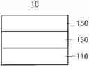
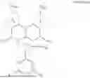

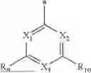

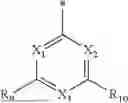


Sources:
- United States Patent and Trademark Office - verify current appl. status at the USPTO↗
Similar patent applications:
- » 20240292742
LIGHT-EMITTING DEVICE INCLUDING HETEROCYCLIC COMPOUND, ELECTRONIC APPARATUS INCLUDING LIGHT-EMITTING DEVICE, AND HETEROCYCLIC COMPOUND - » 20230320208
LIGHT-EMITTING DEVICE INCLUDING HETEROCYCLIC COMPOUND, ELECTRONIC APPARATUS INCLUDING LIGHT-EMITTING DEVICE, AND HETEROCYCLIC COMPOUND - » 20240260462
LIGHT-EMITTING DEVICE INCLUDING HETEROCYCLIC COMPOUND, ELECTRONIC APPARATUS INCLUDING THE LIGHT-EMITTING DEVICE, AND THE HETEROCYCLIC COMPOUND - » 20230209993
LIGHT-EMITTING DEVICE INCLUDING HETEROCYCLIC COMPOUND, ELECTRONIC APPARATUS INCLUDING THE LIGHT-EMITTING DEVICE, AND THE HETEROCYCLIC COMPOUND - » 20240260459
LIGHT-EMITTING DEVICE INCLUDING HETEROCYCLIC COMPOUND, ELECTRONIC APPARATUS INCLUDING THE LIGHT-EMITTING DEVICE, AND THE HETEROCYCLIC COMPOUND - » 20220271227
LIGHT-EMITTING DEVICE INCLUDING HETEROCYCLIC COMPOUND, ELECTRONIC APPARATUS INCLUDING THE LIGHT-EMITTING DEVICE, AND THE HETEROCYCLIC COMPOUND - » 20230159570
LIGHT-EMITTING DEVICE INCLUDING HETEROCYCLIC COMPOUND, ELECTRONIC APPARATUS INCLUDING THE LIGHT-EMITTING DEVICE, AND THE HETEROCYCLIC COMPOUND - » 20230174559
LIGHT-EMITTING DEVICE INCLUDING HETEROCYCLIC COMPOUND, ELECTRONIC APPARATUS INCLUDING THE LIGHT-EMITTING DEVICE, AND THE HETEROCYCLIC COMPOUND - » 20230270001
LIGHT-EMITTING DEVICE INCLUDING HETEROCYCLIC COMPOUND, ELECTRONIC APPARATUS INCLUDING THE LIGHT-EMITTING DEVICE, AND THE HETEROCYCLIC COMPOUND - » 20240224799
LIGHT-EMITTING DEVICE INCLUDING HETEROCYCLIC COMPOUND, ELECTRONIC APPARATUS INCLUDING THE LIGHT-EMITTING DEVICE, AND THE HETEROCYCLIC COMPOUND
Recent applications in this class:
- » 20250366368 2025-11-27
LIGHT EMITTING DEVICE AND FUSED POLYCYCLIC COMPOUND FOR LIGHT EMITTING DEVICE - » 20250359482 2025-11-20
LIGHT-EMITTING DEVICE INCLUDING CONDENSED CYCLIC COMPOUND, ELECTRONIC APPARATUS INCLUDING THE LIGHT-EMITTING DEVICE, AND THE CONDENSED CYCLIC COMPOUND - » 20250359481 2025-11-20
LIGHT-EMITTING DEVICE AND ELECTRONIC APPARATUS INCLUDING THE SAME - » 20250359480 2025-11-20
ORGANIC LIGHT EMITTING DEVICE - » 20250338772 2025-10-30
LIGHT EMITTING ELEMENT, FUSED POLYCYCLIC COMPOUND FOR THE LIGHT EMITTING ELEMENT, AND DISPLAY DEVICE INCLUDING THE LIGHT EMITTING ELEMENT - » 20250331421 2025-10-23
LONG LIFE ORGANIC LIGHT EMITTING MATERIALS AND ORGANIC LIGHT EMITTING DIODE - » 20250311630 2025-10-02
LIGHT-EMITTING DEVICE INCLUDING CONDENSED CYCLIC COMPOUND, ELECTRONIC APPARATUS INCLUDING THE SAME, AND THE CONDENSED CYCLIC COMPOUND - » 20250301908 2025-09-25
BORON-NITROGEN-CONTAINING ORGANIC COMPOUNDS AND USES THEREOF IN ORGANIC ELECTRONIC DEVICES - » 20250301907 2025-09-25
LIGHT-EMITTING DEVICE INCLUDING CONDENSED CYCLIC COMPOUND, ELECTRONIC APPARATUS INCLUDING THE LIGHT-EMITTING DEVICE, AND THE CONDENSED CYCLIC COMPOUND - » 20250287842 2025-09-11
LIGHT EMITTING ELEMENT, POLYCYCLIC COMPOUND FOR THE SAME, AND ELECTRONIC DEVICE INCLUDING THE SAME
Recent applications for this Assignee:
- » 20250366355 2025-11-27
DISPLAY DEVICE AND DISPLAY SYSTEM INCLUDING DISPLAY DEVICE - » 20250366346 2025-11-27
DISPLAY DEVICE, WEARABLE ELECTRONIC DEVICE, AND METHOD OF MANUFACTURING DISPLAY DEVICE - » 20250366344 2025-11-27
DISPLAY DEVICE AND METHOD OF EVALUATING THE SAME - » 20250366329 2025-11-27
DISPLAY DEVICE AND MANUFACTURING METHOD THEREOF - » 20250366308 2025-11-27
LIGHT-EMITTING DEVICE AND ELECTRONIC APPARATUS INCLUDING THE SAME - » 20250366304 2025-11-27
LIGHT EMITTING ELEMENT AND DISPLAY DEVICE INCLUDING THE SAME - » 20250366301 2025-11-27
LIGHT EMITTING ELEMENT, FUSED POLYCYCLIC COMPOUND FOR THE SAME, AND ELECTRONIC APPARATUS INCLUDING THE SAME - » 20250366299 2025-11-27
LIGHT-EMITTING DEVICE INCLUDING ORGANOMETALLIC COMPOUND, ELECTRONIC APPARATUS INCLUDING THE LIGHT-EMITTING DEVICE, AND THE ORGANOMETALLIC COMPOUND - » 20250366289 2025-11-27
DISPLAY DEVICE - » 20250366267 2025-11-27
DISPLAY DEVICE