DRESSER AND METHOD OF MANUFACTURING THE SAME
US20260077451A1
2026-03-19
19/234,787
2025-06-11
Smart Summary: A dresser is made with a base layer called a substrate. On top of this base layer, there is a first layer. There are also raised parts, called convex portions, that stick out higher than the first layer and are made from a different material. These raised parts can be on the base layer or the first layer. Finally, a second layer is added on top of these raised parts. 🚀 TL;DR
Abstract:
In one embodiment, a dresser includes a substrate. The dresser further includes a first layer provided on the substrate. The dresser further includes at least one convex portion provided on the substrate or the first layer, having an upper end that is higher than an upper face of the first layer, and having a composition that is different from a composition of the first layer. The dresser further includes a second layer provided on the at least one convex portion.
Assignee:
- KIOXIA CORPORATION 3,747 🇯🇵 Tokyo, Japan
Applicant:
Interested in similar patents?
Get notified when new applications in this technology area are published.
Classification:
B24B53/12 » CPC main
Devices or means for dressing or conditioning abrasive surfaces Dressing tools; Holders therefor
Description
CROSS REFERENCE TO RELATED APPLICATIONS
This application is based upon and claims the benefit of priority from the prior Japanese Patent Applications No. 2024-159619, filed on Sep. 13, 2024, and No. 2025-082651 filed on May 16, 2025, the entire contents of which are incorporated herein by reference.
FIELD
Embodiments described herein relate to a dresser and a method of manufacturing the same.
BACKGROUND
In a polishing apparatus such as a CMP (Chemical Mechanical Polishing) apparatus, there is a case where a surface of a polishing pad is dressed using a dresser that includes a plurality of convex portions (protrusions) on a substrate. In this case, there arises a problem of how to form these convex portions.
BRIEF DESCRIPTION OF THE DRAWINGS
FIG. 1 is a perspective view showing a configuration of a polishing apparatus of a first embodiment;
FIG. 2 is a perspective view showing a structure of a dresser of the first embodiment;
FIG. 3 is a sectional view showing a structure of a chip of the first embodiment;
FIG. 4 is a plan view showing the structure of the chip of the first embodiment;
FIG. 5 is a plan view showing a structure of a chip of a modification of the first embodiment;
FIGS. 6 to 12 are sectional views showing a method of manufacturing the chip of the first embodiment;
FIGS. 13A and 13B are a plan view and a perspective view showing a method of manufacturing the dresser of the first embodiment;
FIG. 14 is a plan view showing the method of manufacturing the chip of the first embodiment;
FIG. 15 is a plan view showing a method of manufacturing the chip of a modification of the first embodiment;
FIG. 16 is a sectional view showing a structure of a chip of a comparative example of the first embodiment;
FIGS. 17 to 20 are sectional views showing a method of manufacturing the chip of the comparative example of the first embodiment;
FIG. 21 is a sectional view showing a structure of the chip of a second embodiment;
FIG. 22 is a plan view showing the structure of the chip of the second embodiment;
FIG. 23 is a sectional view showing a method of manufacturing the chip of the second embodiment;
FIG. 24 is a plan view showing the method of manufacturing the chip of the second embodiment;
FIGS. 25A to 25D are plan views showing various examples of a method of manufacturing a chip of a third embodiment;
FIG. 26 is a plan view showing a method of manufacturing a chip of a fourth embodiment;
FIG. 27 is a plan view showing a method of manufacturing a chip of a modification of the fourth embodiment; and
FIGS. 28 to 30 are sectional views showing the method of manufacturing the chip of the fourth embodiment; and
FIGS. 31 to 33 are sectional views showing a method of manufacturing a chip of a modification of the first embodiment.
DETAILED DESCRIPTION
Embodiments will now be explained with reference to the accompanying drawings. In FIGS. 1 to 33, the same configurations are given the same signs, and their duplicate description is omitted.
In one embodiment, a dresser includes a substrate. The dresser further includes a first layer provided on the substrate. The dresser further includes at least one convex portion provided on the substrate or the first layer, having an upper end that is higher than an upper face of the first layer, and having a composition that is different from a composition of the first layer. The dresser further includes a second layer provided on the at least one convex portion.
First Embodiment
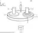
FIG. 1 is a perspective view showing a configuration of a polishing apparatus 10 of a first embodiment. An example of the polishing apparatus 10 is a CMP apparatus.
The polishing apparatus 10 includes a polishing table 11, a dressing mechanism 12, a polishing head 13, a slurry feeding unit 14, and a controlling unit 15.
FIG. 1 shows an X-direction, a Y-direction, and a Z-direction perpendicular to one another. In this specification, the +Z-direction is regarded as the upward direction, and the −Z-direction is regarded as the downward direction. The −Z-direction may coincide with the direction of gravity, and does not have to coincide with the direction of gravity.
The polishing table 11 holds and rotates the polishing pad 1. In FIG. 1, the polishing table 11 holds the polishing pad 1 such that a front face (surface) of the polishing pad 1 is oriented to the +Z-direction, and rotates the polishing pad 1 in the XY-plane.
The dressing mechanism 12 dresses (sets) the polishing pad 1 with a dresser 2. In FIG. 1, the dressing mechanism 12 holds the dresser 2 such that a front face of the dresser 2 is oriented to the −Z-direction, and brings the front face of the dresser 2 into contact with the front face of the polishing pad 1. Thereby, the front face of the polishing pad 1 is dressed by the dresser 2.
The polishing head 13 holds a wafer 3 to be polished by the polishing pad 1. In FIG. 1, the polishing head 13 holds the wafer 3 such that a front face of the wafer 3 is oriented to the −Z-direction, and brings the front face of the wafer 3 into contact with the front face of the polishing pad 1. Thereby, the front face of the wafer 3 is polished by the polishing pad 1. For example, the wafer 3 is used for manufacturing a plurality of semiconductor devices (semiconductor chips).
The slurry feeding unit 14 feeds slurry 4 onto the polishing pad 1. In the polishing apparatus 10, the slurry feeding unit 14 feeds the slurry 4 onto the front face of the polishing pad 1, the polishing table 11 rotates the polishing pad 1, and the polishing head 13 brings the front face of the wafer 3 into contact with the front face of the polishing pad 1. Thereby, the front face of the wafer 3 is polished by the polishing pad 1 onto which the slurry 4 is fed.
The controlling unit 15 controls operation of the polishing apparatus 10. For example, the controlling unit 15 controls rotation of the polishing pad 1 with the polishing table 11, movement of the dresser 2 with the dressing mechanism 12, movement of the wafer 3 with the polishing head 13, feed of the slurry 4 from the slurry feeding unit 14, and the like.
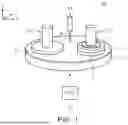
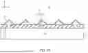
FIG. 2 is a perspective view showing a structure of the dresser 2 of the first embodiment.
The dresser 2 includes a stage metal 21 and one or more chips 22. The stage metal 21 is an example of a chip holding member. The chips 22 are an example of at least one chip. Each of the chips 22 is an example of a first chip.
In FIG. 2, the stage metal 21 has an annular shape, and the one or more chips 22 are arranged into an annular shape on a working face of the stage metal 21. The working face of the stage metal 21 is a face that is to face the polishing pad 1 in FIG. 1. While in FIG. 2, the dresser 2 is arranged in such a manner that the working face of the stage metal 21 is an upper face of the stage metal 21, in FIG. 1, it is held in such a manner that the working face of the stage metal 21 is a lower face of the stage metal 21. In the present embodiment, the surface of the polishing pad 1 is dressed by the chips 22.
For example, the stage metal 21 is formed of stainless steel (SUS) or iron. For example, the chips 22 are manufactured from a wafer 22′ mentioned later (see FIG. 13A). While in FIG. 2, the number of the chips 22 on the stage metal 21 is 12, it may be any other number. Note that, in order to dress the polishing pad 1 uniformly, the number of the chips 22 on the stage metal 21 is desirably two or more and the arrangement of the chips 22 on the stage metal 21 is desirably symmetric.
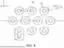
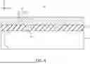
FIG. 3 is a sectional view showing a structure of the chip 22 of the first embodiment.
FIG. 3 shows one of the one or more chips 22 shown in FIG. 2. Each of the chips 22 of the present embodiment has the structure shown in FIG. 3. The chip 22 shown in FIG. 3 includes a substrate 31, a stopper layer 32, one or more convex portions (protrusions) 33, and a thin film 34. The stopper layer 32 is an example of a first layer. The convex portions 33 are an example of at least one convex portion. Each of the convex portions 33 is an example of a first convex portion. The thin film 34 is an example of a second layer.
Hereafter, further details of the chips 22 of the present embodiment are described with reference to FIG. 3. In this description, FIGS. 4 and 5 are also properly referred to. FIG. 4 is a plan view showing the structure of the chip 22 of the first embodiment. FIG. 5 is a plan view showing a structure of the chip 22 of a modification of the first embodiment. FIG. 3 shows a vertical section (XZ-section) taken along the X-X′ line shown in any of FIG. 4 and FIG. 5.
[Substrate 31]
An example of the substrate 31 is a semiconductor substrate such as a Si (silicon) substrate. FIG. 3 shows a front face S1 and a rear face S2 of the substrate 31. In FIG. 3, the front face S1 and the rear face S2 of the substrate 31 are parallel to the X-direction and the Y-direction, and are perpendicular to the Z-direction. The chip 22 shown in FIG. 3 is arranged on the stage metal 21 such that the rear face S2 of the substrate 31 faces the working face of the stage metal 21. An example of the substrate 31 is a Si substrate that has the (111) plane as its orientation.
[Stopper Layer 32]
The stopper layer 32 is formed on the substrate 31. An example of the stopper layer 32 is an insulator such as a SiO2 film (silicon oxide film) or a SiN film (silicon nitride film). Note that the stopper layer 32 may be an insulator other than the SiO2 film and the SiN film, or may be other than an insulator. An example of a thickness of the stopper layer 32 is 20 to 30 μm. The stopper layer 32 of the present embodiment is used as an etching stopper in etching mentioned later.
The stopper layer 32 has one or more concave portions (openings) 32a. These concave portions 32a are arranged, for example, into a shape of a quadrangular grid (FIG. 4). Note that these concave portions 32a may be arranged into a shape of another grid and, for example, may be arranged into a shape of a triangular grid (FIG. 5). FIGS. 4 and 5 show pitches “P” between these concave portions 32a. An example of each of the pitches “P” is 200 to 400 μm. As shown in FIG. 3, the concave portions 32a are formed so as to penetrate the stopper layer 32. The concave portions 32a are an example of at least one concave portion.
[Convex Portion 33]
Each of convex portions 33 is formed on the substrate 31 and the stopper layer 32, and has an upper end that is higher than an upper face of the stopper layer 32. Therefore, the convex portions 33 protrude in the +Z-direction relative to the upper face of the stopper layer 32. An example of the convex portions 33 is a semiconductor layer such as a silicon layer. The convex portions 33 of the present embodiment are formed by epitaxial growth from the substrate 31 as mentioned later. Therefore, the substrate 31 and the convex portions 33 of the present embodiment are formed of the same semiconductor material (for example, silicon). An example of the silicon is single crystal silicon.
In the present embodiment, each convex portion 33 has a composition different from a composition of the stopper layer 32. In the present embodiment, an example of the convex portions 33 is a silicon layer, and an example of the stopper layer 32 is a SiO2 film or a SiN film. This makes it possible to use the stopper layer 32 as the etching stopper when the convex portions 33 are formed from a growth layer 33′ mentioned layer.
Each of the convex portions 33 includes a lower portion 33a and an upper portion 33b. The lower portion 33a is an example of a first portion. The upper portion 33b is an example of a second portion.
As to each of the convex portions 33, the lower portion 33a is formed on the substrate 31 in one concave portion 32a. Therefore, the lower portion 33a is in contact with the front face S1 of the substrate 31. The lower portion 33a of the present embodiment has a cylindrical shape, and accordingly, has a circular shape in plan view and has a vertical section shape of a quadrangle (for example, rectangle). FIG. 4 shows a diameter “D1” of the lower portion 33a.
As to each of the convex portions 33, the upper portion 33b is formed on the lower portion 33a and the stopper layer 32. Therefore, the upper portion 33b has an upper end that is higher than the upper face of the stopper layer 32. The upper portion 33b of the present embodiment has a conical shape, and accordingly, has a circular shape in plan view and has a vertical section shape of a triangle (for example, isosceles triangle). In this case, the upper end of each of the convex portions 33 (upper end of the upper portion 33b) is an apex of the conical shape. FIG. 4 shows a diameter “D2” of the upper portion 33b. In the present embodiment, the diameter “D2” is larger than the diameter “D1”. As a result, as to each of the convex portions 33, an area (π×D22) of the upper portion 33b in plan view is larger than an area (π×D12) of the lower portion 33a in plan view. Moreover, as to each of the convex portions 33 shown in FIG. 3, a width of the upper portion 33b in the X-direction is larger than a width of the lower portion 33a in the X-direction. An example of the diameter “D2” is 200 to 400 μm.
FIG. 3 shows a thickness “T1” of each convex portion 33, a thickness “T2” of the lower portion 33a of each convex portion 33, and a thickness “T3” of the upper portion 33b of each convex portion 33 (T1=T2+T3). An example of the thickness “T2” is 20 to 30 μm. An example of the thickness “T3” is 100 to 150 μm. While in FIG. 3, the thickness “T3” is larger than the thickness “T2”, it may be smaller than the thickness “T2”.
The chip 22 shown in FIG. 3 includes the one or more convex portions 33 that correspond to the one or more concave portions 32a one by one. In FIG. 4, since the concave portions 32a are arranged into the shape of a quadrangular grid, the convex portions 33 are also arranged into a shape of a quadrangular grid. In FIG. 4, pitches between the convex portions 33 are equal to the pitches “P” between the concave portions 32a.
[Thin Film 34]
The thin film 34 is formed on the convex portions 33. The thin film 34 of the present embodiment is continuously formed on the stopper layer 32 and the one or more convex portions 33. An example of the thin film 34 is a C (carbon) layer such as a diamond layer. In the present embodiment, a thickness of the thin film 34 is smaller than the thickness “T2” and the thickness “T3”.
As above, the dresser 2 of the present embodiment includes the one or more convex portions 33 provided on the substrate 31 via the stopper layer 32, and these convex portions 33 are covered by the thin film 34. The dresser 2 of the present embodiment dresses the polishing pad 1 with these convex portions 33 (and the thin film 34).
FIGS. 6 to 12 are sectional views showing a method of manufacturing the chip 22 of the first embodiment.
First, the stopper layer 32 is formed on the substrate 31 (FIG. 6). The stopper layer 32 is formed, for example, by CVD (Chemical Vapor Deposition). Notably, the substrate 31 shown in FIG. 6 is the substrate 31 that is in the state of the wafer 22′ (see FIG. 13A), not the substrate 31 that is in the state of the chip 22. The same holds true for FIGS. 7 to 12 mentioned later.
Next, the one or more concave portions 32a are formed in the stopper layer 32 by lithography and RIE (Reactive Ion Etching) (FIG. 7). As a result, the front face S1 of the substrate 31 is exposed in the concave portions 32a.
Next, the growth layer 33′ is formed on the substrate 31 and the stopper layer 32, and a surface of the growth layer 33′ is flattened by CMP (FIG. 8). For example, the growth layer 33′ is formed by epitaxial growth from the substrate 31. The growth layer 33′ is formed so as to include one or more lower portions 33a′ and an upper portion 33b′. Each of the lower portions 33a′ is formed on the substrate 31 in one concave portion 32a. The upper portion 33b′ is formed on the one or more lower portions 33a′ and the stopper layer 32. An example of the growth layer 33′ is a semiconductor layer such as a silicon layer. The growth layer 33′ is an example of a third layer.
Next, a mask layer 35 is formed on the growth layer 33′ (FIG. 9). In FIG. 9, the mask layer 35 includes a lower mask layer 41 formed on the growth layer 33′ and an upper mask layer 42 formed on the lower mask layer 41. An example of the lower mask layer 41 is a TEOS (tetraethyl orthosilicate) layer formed by CVD. The lower mask layer 41 may be a SiO2 layer or a carbon layer formed by plasma CVD. An example of the upper mask layer 42 is a resist layer. The mask layer 35 is an example of a fourth layer.
Next, the mask layer 35 is processed by lithography and RIE (FIG. 10). In FIG. 10, by forming an opening 35b in the mask layer 35, one or more mask portions 35a are formed from the mask layer 35. As a result, the surface of the growth layer 33′ is exposed in the opening 35b of the mask layer 35. Each of the mask portions 35a includes a mask portion 41a formed from the lower mask layer 41 and a mask portion 42a formed from the upper mask layer 42. The opening 35b includes an opening 41b formed in the lower mask layer 41 and an opening 42b formed in the upper mask layer 42.
Each of the mask portions 35a of the present embodiment is etched into a cylindrical shape as with the lower portion 33a of each of the convex portions 33 shown in FIG. 3. Therefore, each of the mask portions 35a of the present embodiment has a circular shape in plan view and has a vertical section shape of a quadrangle (for example, rectangle). Further details of the mask portions 35a are described later with reference to FIGS. 14 and 15.
Next, the growth layer 33′ is etched by dry etching using the mask layer 35 (FIG. 11). As a result, an opening H1 is formed in the growth layer 33′ beneath the opening 35b, and the one or more convex portions 33 are formed from the growth layer 33′. Each of the convex portions 33 is formed so as to include the lower portion 33a formed from the lower portion 33a′, and the upper portion 33b formed from the upper portion 33b′. Since each of the convex portions 33 includes the upper portion 33b, it has the upper end that is higher than the upper face of the stopper layer 32. The dry etching in FIG. 11 is performed until the upper face of the stopper layer 32 is exposed.
In the dry etching in FIG. 11, the stopper layer 32 is used as an etching stopper. Therefore, the stopper layer 32 is desirably a layer that has a high etching ratio between the stopper layer 32 and the growth layer 33′. The dry etching in FIG. 11 is performed, for example, using mixture gas containing SF6 gas, C4F8 gas, and O2 gas (S, F, C, and O denote sulfur, fluorine, carbon, and oxygen, respectively). Notably, when the lower mask layer 41 is a carbon layer, the dry etching in FIG. 11 may be performed, for example, using mixture gas containing any of HBr gas, Cl2 gas, and NF3 gas and O2 gas (H, Br, Cl, and N denote hydrogen, bromine, chlorine, and nitrogen, respectively). Each of the convex portions 33 of the present embodiment is processed so as to include the lower portion 33a having the cylindrical shape and the upper portion 33b having the conical shape.
The mask layer 35 is removed after this dry etching is performed. Notably the mask portions 35a may drop and come down between the convex portions 33 during this dry etching being performed or after this being performed. In this case, the mask layer 35, together with the dropped mask portions 35a, is removed. The mask layer 35 of the present embodiment is removed by a chemical liquid treatment. For example, this chemical liquid treatment may be performed using an aqueous hydrofluoric acid solution, or may be performed using a liquid mixture of sulfuric acid and aqueous hydrogen peroxide. There is a case where, in this liquid chemical treatment, the upper face of the stopper layer 32 is partially etched.
Next, the thin film 34 is formed on the one or more convex portions 33 formed from the growth layer 33′ (FIG. 12). The thin film 34 of the present embodiment is continuously formed on the stopper layer 32 and the one or more convex portions 33. An example of the thin film 34 is a diamond layer formed by plasma CVD under a high temperature condition.
Notably, there is a case where, due to the dry etching in FIG. 11, the stopper layer 32 is partially etched. As a result, in FIG. 12, there is a case where an upper face of a region, of the stopper layer 32, which region is not covered by any of the convex portions 33 is lower than an upper face of a region, of the stopper layer 32, which region is covered by any of convex portions 33.
FIGS. 13A and 13B are a plan view and a perspective view showing a method of manufacturing the dresser 2 of the first embodiment.
FIG. 13A shows the wafer 22′ after the step shown in FIG. 12 is performed. In the present embodiment, the wafer 22′ is divided into a plurality of chips 22 by dicing. Each of the chips 22 has the structure shown in FIG. 3 or FIG. 12.
Next, the one or more chips 22 are mounted on the stage metal 21 (FIG. 13B). These chips 22 mounted on the stage metal 21 may be manufactured from the same wafer 22′, or may be manufactured from a different wafer 22′. As above, the dresser 2 shown in FIG. 2 is manufactured.
Notably, the step shown in FIG. 12 may be performed between the step shown in FIG. 13A and the step shown in FIG. 13B, in place of being performed before the step shown in FIG. 13A. In other words, the thin film 34 may be formed above the substrates 31 included in the wafer 22′ before the dicing, or may be formed above the substrate 31 included in each of the chips 22 after the dicing. In the former case, for example, a manufacturer of the dresser 2 may prepare (for example, manufacture or purchase) the wafer 22′ on which the thin film 34 is provided, and sequentially perform, on the prepared wafer 22′, the steps shown in FIGS. 13A and 13B. In the latter case, for example, the manufacturer of the dresser 2 may prepare (for example, manufacture or purchase) the wafer 22′ on which the thin film 34 is not provided, and sequentially perform the steps shown in FIGS. 13A, 12, and 13B on the prepared wafer 22′. An example of such a process is described with reference to FIGS. 31 to 33.
FIGS. 31 to 33 are sectional views showing a method of manufacturing a chip of a modification of the first embodiment. FIGS. 31 to 33 are explained by distinguishing the substrate 31 in a state of the wafer 22′ and the substrate 31 in a state of a chip 22.
FIG. 31 shows the substrate 31 and the like after performing the step shown in FIG. 11 and before performing the step shown in FIG. 12. The substrate in FIG. 31 is in the state of the wafer 22′.
Next, the step shown in FIG. 13A is performed to divide the wafer 22′ into the plurality of chips 22. FIG. 32 shows one of these chips 22. FIG. 32 shows the front face S1, the rear face S2 and a side face S3 of the substrate 31 in the state of the chip 22.
Next, the step shown in FIG. 12 is performed to form the thin film 34 on the one or more convex portions 33. FIG. 33 shows the thin film 34 formed in such a way. The thin film 34 of the present modification is also formed on the side face S3 of the substrate 31 and a side face of the stopper layer 32. Moreover, the thin film 34 of the present modification may also be formed on the rear face S2 of the substrate 31. As shown in FIG. 33, the thin film 34 of the present modification is continuously formed on the surfaces of the convex portions 33, the upper face of the stopper layer 32, and the side face of the stopper layer 32. The thin film 34 of the present modification may be continuously formed on the surfaces of the convex portions 33, the upper face of the stopper layer 32, the side face of the stopper layer 32, the side face S3 of the substrate 31, and the rear face S2 of the substrate 31.
FIG. 33 shows corner portions (edge portions) K of the thin film 34. The corner portions K of the thin film 34 are located between the upper face and the side face of the thin film 34. In the present modification, the thin film 34 is formed after the wafer 22′ is divided into the plurality of the chips 22, and therefore the corner portions K of the thin film 34 have round shapes. Moreover, the thin film 34 is formed to continuously cover the upper face and the side face of the stopper layer 32. This makes it possible to prevent the thin film 34 from breaking from the corner portions K.
In the present modification, the step shown in FIG. 13B is then performed. In this way, the dresser shown in FIG. 2 is manufactured.
FIG. 14 is a plan view showing the method of manufacturing the chip 22 of the first embodiment. FIG. 15 is a plan view showing a method of manufacturing the chip 22 of a modification of the first embodiment.
FIG. 14 shows the one or more mask portions 35a and the opening 35b in the mask layer 35 shown in FIG. 10. FIG. 14 further shows, for comparison, the one or more convex portions 33 formed in the step shown in FIG. 11 with broken lines. As with FIG. 4, FIG. 14 shows the diameter “D1” of the lower portion 33a of each of the convex portions and the diameter “D2” of the upper portion 33b of each of the convex portions. FIG. 14 further shows a diameter “D3” of each of the mask portions 35a shown in FIG. 10. In the present embodiment, the diameter “D3” is set to be larger than the diameter “D2”.
Notably, the one or more mask portions 35a in the mask layer 35 may be formed into a shape of a quadrangular grid as shown in FIG. 14, or may be formed into a shape of a triangular grid as shown in FIG. 15. Moreover, these mask portions 35a may be formed into a shape of another grid.
Next, the chip 22 of a comparative example of the present embodiment is described with reference to FIGS. 16 to 20.
FIG. 16 is a sectional view showing a structure of the chip 22 of the comparative example of the first embodiment.
The chip 22 of the first embodiment (FIG. 3) includes the substrate 31, the stopper layer 32, the one or more convex portions 33, and the thin film 34. On the other hand, the chip 22 of the present comparative example (FIG. 16) includes the substrate 31 and the thin film 34.
The substrate 31 of the present comparative example includes a lower portion 31a and one or more upper portions 31b formed on the lower portion 31a, and the thin film 34 of the present comparative example is continuously formed on these upper portions 31b. Each of the upper portions 31b has a conical shape as with the upper portion 33b of each of the convex portions 33 of the first embodiment. FIG. 16 shows a thickness “T1′” of each of the upper portions 31b. An example of the thickness “T1′” is 100 to 150 μm.
The dresser 2 of the present comparative example has the structure shown in FIG. 2 as with the dresser 2 of the first embodiment. Note that the dresser 2 of the present comparative example includes the one or more upper portions 31b as portions of the substrate 31, and these upper portions 31b are covered by the thin film 34. The dresser 2 of the present comparative example dresses the polishing pad 1 with these upper portions 31b (and the thin film 34).
FIGS. 17 to 20 are sectional views showing a method of manufacturing the chip 22 of the comparative example of the first embodiment.
First, the mask layer 35 is formed on the substrate 31 (FIG. 17). In FIG. 17, the mask layer 35 includes the lower mask layer 41 and the upper mask layer 42.
Next, the mask layer 35 is processed by lithography and RIE (FIG. 18). In FIG. 18, by forming the opening 35b in the mask layer 35, the one or more mask portions 35a are formed from the mask layer 35. As a result, the front face S1 of the substrate 31 is exposed in the opening 35b of the mask layer 35. Each of the mask portions 35a includes the mask portion 41a in the lower mask layer 41, and the mask portion 42a in the upper mask layer 42. The opening 35b includes the opening 41b in the lower mask layer 41, and the opening 42b in the upper mask layer 42.
Next, the substrate 31 is etched by dry etching using the mask layer 35 (FIG. 19). As a result, a recess portion H2 is formed in the substrate 31 beneath the opening 35b, and the lower portion 31a and the one or more upper portions 31b are formed in the substrate 31. The mask layer 35 is removed after this dry etching.
Next, the thin film 34 is continuously formed on the one or more upper portions 31b formed in the substrate 31 (FIG. 20). An example of the thin film 34 of the present comparative example is a diamond layer as with the first embodiment.
Next, the chip 22 of the first embodiment and the chip 22 of the comparative example of the first embodiment are compared with each other.
In the comparative example, for dressing the polishing pad 1, the one or more upper portions 31b are formed in the substrate 31. In the comparative example, a pitch “P” between the upper portions 31b determine the thickness “T1′” of each of the upper portions 31b. For example, as the pitch “P” is larger, the thickness “T1′” is also larger. Meanwhile, in order to set a density of the upper portions 31b on the front face of the dresser 2 to a predetermined value, the pitch “P” is often set to a predetermined value, which results in determining the thickness “T1′”. Therefore, in the comparative example, the thickness “T1′” is often not able to be flexibly set.
When the thickness “T1′” is too large, there arises a problem that a pad cut rate of the polishing pad 1 in dressing becomes large. The pad cut rate is a decrease amount of the thickness of the polishing pad 1 per unit time. When the thickness “T1′” is too large, the polishing pad 1 wears away in a short time, which raises costs of the polishing pad 1.
Moreover, when the thickness “T1′” is too small, there arises a problem that roughness of the front face of the polishing pad 1 in dressing does not become sufficiently large. When the roughness of the polishing pad 1 is too small, polishing performance of the polishing pad 1 lowers. Conversely, when the thickness “T1′” is too large, there arises a problem that the roughness of the front face of the polishing pad 1 in dressing becomes too large. When the roughness of the polishing pad 1 is too large, dusts, along with particles of the slurry 4, come between convex portions and/or into concave portions on the front face of the polishing pad 1.
On the other hand, in the present embodiment, for dressing the polishing pad 1, the one or more convex portions 33 are formed on the substrate 31 via the stopper layer 32. While in the comparative example, the upper portions 31b contribute to dressing, the upper portions 33b of the convex portions 33 contribute to dressing in the present embodiment. The present embodiment makes it possible to determine the thickness “T3” of the upper portion 33b of each convex portion 33 independently of the pitch “P” between the convex portions 33. The reason is that the thickness “T3” of the upper portion 33b of each convex portion 33 can be adjusted by adjusting the thickness of the stopper layer 32, that is, the thickness “T2” of the lower portion 33a of each convex portion 33. Therefore, the present embodiment makes it possible to reduce the pad cut rate of the polishing pad 1 in dressing by setting the thickness “T3” to an appropriate value and/or to adjusting the roughness of the front face of the polishing pad 1 in dressing to an appropriate value.
As above, the dresser 2 of the present embodiment includes the one or more convex portions 33 provided on the substrate 31 via the stopper layer 32, and these convex portions 33 are covered by the thin film 34. Therefore, the present embodiment makes it possible to implement the convex portions 33 preferable for dressing. For example, the thickness “T3” of the upper portion 33b of each convex portion 33 can be determined independently of the pitch “P” between the convex portions 33.
Notably, the dresser 2 of the present embodiment includes, for example, a SiO2 film or a SiN film as the stopper layer 32. Since this SiO2 film or SiN film is the stopper layer 32 formed for being used as an etching stopper, in the present embodiment, this SiO2 film or SiN film is used as the etching stopper. On the other hand, neither the SiO2 film nor the SiN film may be used as the etching stopper, and they may be formed for another purpose. Such a SiO2 film or a SiN film is also an example of the first layer. Moreover, the dresser 2 of the present embodiment may include the thin film 34 that is other than a diamond layer. The thin film 34 that is other than a diamond layer is also an example of the second layer.
Second Embodiment
FIG. 21 is a sectional view showing a structure of the chip 22 of a second embodiment.
The chip 22 of the present embodiment (FIG. 21) includes the substrate 31, the stopper layer 32, the one or more convex portions 33, and the thin film 34 as with the chip 22 of the first embodiment (FIG. 3). Nevertheless, in the chip 22 of the present embodiment, the number of the concave portions 32a in the stopper layer 32 is smaller than the number of the convex portions 33.
Therefore, the chip 22 of the present embodiment includes the convex portions 33 each of which includes the lower portion 33a and the upper portion 33b and the convex portions 33 each of which includes only the upper portion 33b. The former convex portions 33 are formed on the substrate 31 and the stopper layer 32 and is in contact with the substrate 31, and the latter convex portions 33 are formed on the stopper layer 32 and is not in contact with the substrate 31. Each of the former convex portions 33 is an example of a first convex portion, and each of the latter convex portions 33 is an example of a second convex portion.
FIG. 22 is a plan view showing the structure of the chip 22 of the second embodiment.
FIG. 22 shows the concave portions 32a and the convex portions 33 arranged into a shape of a quadrangular grid as with FIG. 4. Note that the chip 22 shown in FIG. 22 includes the convex portions 33 that are arranged so as to overlap with the concave portions 32a in plan view and the convex portions 33 that are arranged so as not to overlap with the concave portions 32a in plan view.
FIG. 23 is a sectional view showing a method of manufacturing the chip 22 of the second embodiment.
FIG. 23 shows a section corresponding to FIG. 10. The chip 22 of the present embodiment can be manufactured by the steps shown in FIGS. 6 to 12 as with the chip 22 of the first embodiment. Note that the growth layer 33′ and the mask layer 35 in the present embodiment are formed such that the number of the concave portions 32a is smaller than the number of the mask portions 35a. For example, the growth layer 33′ of the present embodiment is formed by epitaxial growth from the substrate 31 as with the growth layer 33′ of the first embodiment. The present embodiment makes it possible to form both the convex portions 33 that overlap with the concave portions 32a in plan view and the convex portions 33 that do not overlap with the concave portions 32a in plan view by epitaxial growth from the substrate 31 exposed in the concave portions 32a.
FIG. 24 is a plan view showing the method of manufacturing the chip 22 of the second embodiment.
FIG. 24 shows the one or more mask portions 35a and the opening 35b in the mask layer 35 shown in FIG. 23. FIG. 24 further shows, for comparison, the one or more convex portions 33 formed after the step shown in FIG. 23 with broken lines.
Shapes of the mask portions 35a and the opening 35b shown in FIG. 24 are the same as the shapes of the mask portions 35a and the opening 35b shown in FIG. 14. Note that the mask layer 35 shown in FIG. 24 includes the mask portions 35a that are arrange so as to overlap with the concave portions 32a in plan view and the mask portions 35a that are arranged so as not to overlap with the concave portions 32a in plan view.
Notably, each of the concave portions 32a is desirably arranged so as to overlap with any of the convex portions 33 in plan view. The reason is that, if a certain concave portion 32a is arranged so as to overlap with none of the convex portions 33 in plan view, this causes the growth layer 33′ that is formed in that concave portion 32a to be removed in etching the growth layer 33′, and causes the substrate 31 to be exposed in that concave portion 32a.
The present embodiment makes it possible to implement the convex portions 33 preferable for dressing, using the concave portions 32a that are smaller in number than the convex portions 33.
Notably, while the chip 22 of the present embodiment includes the convex portions 33 that are in contact with the substrate 31 and the convex portions 33 that are not in contact with the substrate 31, it may include only the convex portions 33 that are not in contact with the substrate 31. Examples of such a chip 22 are described in third and fourth embodiments mentioned later.
Third Embodiment
FIGS. 25A to 25D are plan views showing various examples of a method of manufacturing the chip 22 of the third embodiment.
FIG. 25A shows a first example of the method of manufacturing the chip 22 of the present embodiment. More in detail, FIG. 25A shows the wafer 22′ before being diced into the plurality of chips 22, the stopper layer 32 included in the wafer 22′, and the plurality of concave portions 32a formed in the stopper layer 32. FIG. 25A shows the stopper layer 32 with dot hatching and the concave portions 32a to be white. Likewise, FIGS. 25B, 25C, and 25D show second, third, and fourth examples of the method of manufacturing the chip 22 of the present embodiment, respectively.
In the first example, the plurality of concave portions 32a are arranged on two straight lines passing through the center of the wafer 22′. In the second example, the plurality of concave portions 32a are arranged on one circumference enclosing the center of the wafer 22′. In the third example, the plurality of concave portions 32a are arranged on four straight lines passing through the center of the wafer 22′. In the fourth example, the plurality of concave portions 32a are arranged on two circumferences enclosing the center of the wafer 22′.
In each of the first to fourth examples, the wafer 22′ may include the chips 22 that include the concave portions 32a, and the chips 22 that do not include the concave portions 32a.
As with the second embodiment, the present embodiment makes it possible to implement the convex portions 33 preferable for dressing, using the concave portions 32a that are smaller in number than the convex portions 33.
Fourth Embodiment
FIG. 26 is a plan view showing a method of manufacturing the chip 22 of the fourth embodiment.
FIG. 26 shows the wafer 22′ before being diced into the plurality of chips 22, a plurality of chip regions R1 in the wafer 22′, and a scribe (dicing) region R2 in the wafer 22′. Each of the chip regions R1 has a shape of a quadrangular (for example, square or rectangle) in plan view. In plan view, the scribe region R2 has a shape of a mesh formed by combining a plurality of straight line portions extending in the X-direction and a plurality of straight line portions extending in the Y-direction. In the present embodiment, by cutting the wafer 22′ along the scribe region R2, each of the chip regions R1 becomes one chip 22.
FIG. 26 further shows the stopper layer 32 included in the wafer 22′, and the concave portion 32a formed in the stopper layer 32. FIG. 26 shows the stopper layer 32 with dot hatching and the concave portion 32a to be white. The concave portion 32a of the present embodiment has a shape of a mesh in plan view, having the same planar shape as the planar shape of the scribe region R2. Therefore, the stopper layer 32 of the present embodiment is divided into the equal number of portions to the number of the chip regions R1. Each of the portions of the stopper layer 32 of the present embodiment has a quadrangular shape in plan view, having the same planar shape as the planar shape of one chip region R1. Therefore, each of the chips 22 of the present embodiment is manufactured so as not to include the concave portion 32a in the stopper layer 32. This is because the concave portion 32a are formed only in the scribe region R2.
FIG. 27 is a plan view showing a method of manufacturing the chip 22 of a modification of the fourth embodiment.
FIG. 27 also shows the wafer 22′ before being diced into the plurality of chips 22, the plurality of chip regions R1 in the wafer 22′, and the scribe region R2 in the wafer 22′. FIG. 27 further shows the stopper layer 32 included in the wafer 22′, and the plurality of concave portions 32a formed in the stopper layer 32. The concave portions 32a of the present modification are formed in the scribe region R2. Therefore, each of the chips 22 of the present modification is also manufactured so as not to include the concave portions 32a in the stopper layer 32.
FIGS. 28 to 30 are sectional views showing the method of manufacturing the chip 22 of the fourth embodiment.
FIG. 28 shows a section corresponding to FIG. 10. Note that FIG. 28 shows the plurality of chip regions R1 and the scribe region R2 in the wafer 22′. The concave portion 32a shown in FIG. 28 has a shape of a mesh in plan view, having the same planar shape as the planar shape of the scribe region R2.
Next, the growth layer 33′ is etched by dry etching using the mask layer 35 (FIG. 29). As a result, the opening H1 is formed in the growth layer 33′ beneath the opening 35b, and the one or more convex portions 33 are formed from the growth layer 33′. Each of the convex portions 33 is formed so as to include the upper portion 33b formed from the upper portion 33b′ and not to include the lower portion 33a formed from the lower portion 33a′. Since each of the convex portions 33 include the upper portion 33b, it has the upper end that is higher than the upper face of the stopper layer 32. The mask layer 35 is removed after this dry etching is performed.
In the step shown in FIG. 29, the growth layer 33′ formed in the concave portion 32a is removed, and the substrate 31 is exposed in the concave portion 32a. Therefore, in FIG. 29, the front face S1 of the substrate 31 beneath the concave portion 32a is recessed by the aforementioned dry etching.
Next, the thin film 34 is formed on the one or more convex portions 33 formed from the growth layer 33′ (FIG. 30). The thin film 34 of the present embodiment is continuously formed on the stopper layer 32 and the one or more convex portions 33. The thin film 34 of the present embodiment is also further formed on side faces of the stopper layer 32 in the concave portion 32a and on the front face S1 and side faces of the substrate 31 beneath the concave portion 32a.
After that, the wafer 22′ is processed by the steps shown in FIGS. 13A and 13B. As above, the dresser 2 of the present embodiment is manufactured.
The present embodiment makes it possible to implement the convex portions 33 preferable for dressing, using the one or more concave portions 32a in the scribe region R2.
While certain embodiments have been described, these embodiments have been presented by way of example only, and are not intended to limit the scope of the inventions. Indeed, the novel dressers and methods described herein may be embodied in a variety of other forms; furthermore, various omissions, substitutions and changes in the form of the dressers and methods described herein may be made without departing from the spirit of the inventions. The accompanying claims and their equivalents are intended to cover such forms or modifications as would fall within the scope and spirit of the inventions.
Claims
1. A dresser comprising:
a substrate;
a first layer provided on the substrate;
at least one convex portion provided on the substrate or the first layer, having an upper end that is higher than an upper face of the first layer, and having a composition that is different from a composition of the first layer; and
a second layer provided on the at least one convex portion.
2. The dresser of claim 1, wherein the at least one convex portion includes at least any of:
a first convex portion provided on the substrate so as to be in contact with the substrate; and
a second convex portion provided on the first layer so as not to be in contact with the substrate.
3. The dresser of claim 1, wherein a first convex portion of the at least one convex portion includes:
a first portion provided on the substrate in the first layer; and
a second portion provided on the first portion and having an upper end that is higher than the upper face of the first layer.
4. The dresser of claim 3, wherein an area of the second portion in plan view is larger than an area of the first portion in plan view.
5. The dresser of claim 3, wherein the second portion is provided on the first portion and the first layer.
6. The dresser of claim 3, wherein a shape of a vertical section of the second portion is a triangle.
7. The dresser of claim 1, wherein
the substrate is a semiconductor substrate, and
the at least one convex portion is formed of a semiconductor material.
8. The dresser of claim 1, wherein the substrate and the at least one convex portion are formed of the same semiconductor material.
9. The dresser of claim 1, wherein
the first layer is an insulator, and
the second layer is a diamond layer.
10. The dresser of claim 1, wherein the second layer is provided on the at least one convex portion and the first layer, or provided on the at least one convex portion and the first layer and on side faces of the substrate and the first layer.
11. The dresser of claim 1, further comprising:
a chip holding member; and
at least one chip provided on the chip holding member,
wherein a first chip of the at least one chip includes the substrate, the first layer, the at least one convex portion, and the second layer.
12. A method of manufacturing a dresser, comprising:
forming a first layer on a substrate;
forming, on the substrate or the first layer, a third layer having a composition that is different from a composition of the first layer;
etching the third layer until the first layer is exposed, to form at least one convex portion from the third layer; and
forming a second layer on the at least one convex portion.
13. The method of claim 12, wherein a first convex portion of the at least one convex portion is formed by:
forming a first portion of the first convex portion on the substrate in the first layer, and
forming, on the first portion, a second portion of the first convex portion such that the second portion has an upper end that is higher than an upper face of the first layer.
14. The method of claim 12, wherein the third layer is formed by epitaxial growth from the substrate.
15. The method of claim 12, further comprising forming at least one concave portion in the first layer before forming the third layer,
wherein the third layer is formed in the at least one concave portion and on the first layer.
16. The method of claim 12, further comprising:
forming a fourth layer on the third layer before etching the third layer;
etching the third layer using the fourth layer to form the at least one convex portion from the third layer; and
removing the fourth layer after etching the third layer.
17. The method of claim 12, further comprising:
manufacturing at least one chip; and
arranging the at least one chip on a chip holding member,
wherein a first chip of the at least one chip is manufactured so as to include the substrate, the first layer, the at least one convex portion, and the second layer.
18. A method of manufacturing a dresser, comprising:
preparing a wafer including a substrate, a first layer provided on the substrate, and at least one convex portion provided on the substrate or the first layer and having a composition that is different from a composition of the first layer;
manufacturing at least one chip from the wafer; and
arranging the at least one chip on a chip holding member.
19. The method of claim 18, further comprising:
forming a second layer on the at least one convex portion after preparing the wafer; and
manufacturing, from the wafer, a first chip including the substrate, the first layer, the at least one convex portion, and the second layer after forming the second layer.
20. The method of claim 18, further comprising:
manufacturing, from the wafer, a first chip including the substrate, the first layer, and the at least one convex portion after preparing the wafer; and
forming a second layer on the at least one convex portion after manufacturing the first chip.
Images & Drawings included:


Sources:
- United States Patent and Trademark Office - verify current appl. status at the USPTO↗
Similar patent applications:
- » 20180056482
Dresser, method of manufacturing dresser, and method of manufacturing semiconductor device - » 20140302757
Rotary dresser and manufacturing method therefor - » 20250360598
METHOD OF MANUFACTURING GRINDSTONE, GRINDSTONE, METHOD OF MANUFACTURING DRESSER BOARD, AND DRESSER BOARD - » 20250242468
Chemical Mechanical Polishing Pad Dresser and Manufacturing Method Thereof - » 20250242470
Chemical Mechanical Polishing Pad Dresser and Manufacturing Method Thereof - » 20250242469
Chemical Mechanical Polishing Pad Dresser and Manufacturing Method Thereof - » 20250262717
LIGHTWEIGHT GEAR AND MANUFACTURING METHOD OF PAD DRESSER USING WATER JET - » 20250196291
ROTARY DRESSER AND METHOD OF MANUFACTURING THE SAME - » 20190300439
Polycrystalline diamond and method for manufacturing same, scribe tool, scribe wheel, dresser, rotating tool, wire drawing die, cutting tool, electrode, and processing method using polycrystalline diamond - » 20200062601
Polycrystalline diamond and method for manufacturing same, scribe tool, scribe wheel, dresser, rotating tool, orifice for water jet, wire drawing die, cutting tool, electrode, and processing method using polycrystalline diamond
Recent applications in this class:
- » 20250387877 2025-12-25
DRESSING APPARATUS, DRESSING METHOD, AND METHOD OF MANUFACTURING DEVICE CHIPS - » 20250269493 2025-08-28
CHEMICAL MECHANICAL POLISHING APPARATUS, METHOD OF CONDITIONING POLISHING PAD FOR CHEMICAL MECHANICAL POLISHING, CONDITIONING ASSEMBLY FOR CONDITIONING POLISHING PAD USED IN CHEMICAL MECHANICAL POLISHING - » 20250262717 2025-08-21
LIGHTWEIGHT GEAR AND MANUFACTURING METHOD OF PAD DRESSER USING WATER JET - » 20250196291 2025-06-19
ROTARY DRESSER AND METHOD OF MANUFACTURING THE SAME - » 20240189962 2024-06-13
DRESSING MEMBER - » 20240173820 2024-05-30
CONDITIONER AND CHEMICAL MECHANICAL POLISHING APPARATUS INCLUDING THE SAME - » 20230294241 2023-09-21
POLISHING METHOD AND POLISHING APPARATUS - » 20230051072 2023-02-16
DRESSING RING - » 20220379433 2022-12-01
POLISHING SYSTEM AND DRESSING DEVICE THEREOF - » 20220314398 2022-10-06
Dressing Tool and Method for the Production Thereof
Recent applications for this Assignee:
- » 20260083028 2026-03-19
SEMICONDUCTOR DEVICE AND METHOD OF MANUFACTURING SEMICONDUCTOR DEVICE - » 20260083001 2026-03-19
SEMICONDUCTOR STORAGE DEVICE - » 20260082930 2026-03-19
SEMICONDUCTOR INTEGRATED CIRCUIT AND RECEIVING DEVICE - » 20260082817 2026-03-19
MAGNETIC MEMORY DEVICE - » 20260082813 2026-03-19
MEMORY DEVICE - » 20260082812 2026-03-19
MAGNETIC MEMORY DEVICE - » 20260082672 2026-03-19
SEMICONDUCTOR MEMORY DEVICE - » 20260082651 2026-03-19
SEMICONDUCTOR STORAGE DEVICE - » 20260082590 2026-03-19
SEMICONDUCTOR DEVICE AND METHOD OF MANUFACTURING SEMICONDUCTOR DEVICE - » 20260082584 2026-03-19
MEMORY DEVICE