DECISION FEEDBACK EQUALIZER AND METHOD FOR PERFORMING DECISION FEEDBACK EQUALIZATION ON INPUT SIGNAL IN DECISION FEEDBACK EQUALIZER
US20260095352A1
2026-04-02
19/317,115
2025-09-02
Smart Summary: A decision feedback equalizer (DFE) helps improve the quality of signals by correcting errors in the received data. It uses two comparators to compare signals against specific thresholds and generate comparison results. The first comparator works with a signal that is delayed based on the first comparison result, while the second comparator does the same with a different signal. Each comparator has its own calculation circuit that processes the input signal and the delayed results. This method allows for better decision-making in interpreting the input signals. 🚀 TL;DR
Abstract:
A decision feedback equalizer (DFE) and a method for performing decision feedback equalization on an input signal in the DFE are provided. The DFE includes a first comparator, a first calculating circuit, a second comparator and a second calculating circuit. The first comparator is configured to compare a first calculation signal with a first threshold to generate a first comparison result, and the first calculating circuit is configured to generate the first calculation signal according to the input signal and a first delayed signal of the first comparison result. The second comparator is configured to compare a second calculation signal with a second threshold to generate a second comparison result, and the second calculating circuit is configured to generate the second calculation signal according to the input signal and a second delayed signal of the second comparison result.
Assignee:
- REALTEK SEMICONDUCTOR CORP. 2,080 🇹🇼 Hsinchu, Taiwan
Applicant:
Interested in similar patents?
Get notified when new applications in this technology area are published.
Classification:
H04L25/03885 » CPC main
Baseband systems; Details ; arrangements for supplying electrical power along data transmission lines; Shaping networks in transmitter or receiver, e.g. adaptive shaping networks; Line equalisers; line build-out devices adaptive
H04L25/03 IPC
Baseband systems; Details ; arrangements for supplying electrical power along data transmission lines Shaping networks in transmitter or receiver, e.g. adaptive shaping networks
Description
BACKGROUND OF THE INVENTION
1. Field of the Invention
The present invention is related to X-level pulse amplitude modulation (PAMX) circuits, and more particularly, to a decision feedback equalizer (DFE) and a method for performing decision feedback equalization on an input signal in the DFE.
2. Description of the Prior Art
A typical non-return-to-zero (NRZ) circuit such as a two-level pulse-amplitude modulation (PAM2) circuit has a differential input signal with two possible states. In comparison with a PAM2 circuit, an X-level pulse-amplitude modulation (PAMX) circuit has a differential input signal with X possible states, where X is a positive integer greater than two. For example, the differential input signal of a PAM3 circuit may have three possible states, and the differential input signal of a PAM4 circuit may have four possible states, where the rest may be deduced by analogy. Taking the PAM3 circuit as an example, the possible states of the differential input signal may include a high level, a middle level, and a low level. When the differential input signal is at a middle level, the PAM3 circuit of the related art typically avoids performing decision feedback equalization operations, which makes an overall decision feedback equalization effect of the PAM3 circuit insufficient.
Furthermore, in order to effectively reduce a circuit area, some calculation circuits or logics can be integrated together. The wiring for integrating the calculation circuits and logics of a decision feedback equalizer (DFE) within the PAMX circuit of the related art will be quite complicated, and therefore not conducive to integrating internal sub-circuits thereof.
Thus, there is a need for a novel DFE, which can solve the problem of the related art without introducing any side effect or in a way that is less likely to introduce side effects.
SUMMARY OF THE INVENTION
An objective of the present invention is to provide a decision feedback equalizer (DFE) and a method for performing decision feedback equalization on an input signal in the DFE, in order to improve the effect of decision feedback equalization.
Another objective of the present invention is to provide a DFE and a method for performing decision feedback equalization on an input signal in the DFE, in order to solve the related art problem of wiring complexity introduced in circuit integration.
At least one embodiment of the present invention provides a DFE. The DFE comprises a first comparator, a first calculating circuit, a second comparator and a second calculating circuit, where the first calculating circuit is coupled to the first comparator, and the second calculating circuit is coupled to the second comparator. The first comparator is configured to compare a first calculation signal with a first threshold to generate a first comparison result, and the first calculating circuit is configured to generate the first calculation signal according to an input signal and a first delayed signal of the first comparison result. The second comparator is configured to compare a second calculation signal with a second threshold to generate a second comparison result, and the second calculating circuit is configured to generate the second calculation signal according to the input signal and a second delayed signal of the second comparison result.
At least one embodiment of the present invention provides a method for performing decision feedback equalization on an input signal in a DFE. The method comprises: utilizing a first comparator of the DFE to compare a first calculation signal with a first threshold to generate a first comparison result, wherein the first calculation signal is generated according to the input signal and a first delayed signal of the first comparison result by a first calculating circuit of the DFE; and utilizing a second comparator of the DFE to compare a second calculation signal with a second threshold to generate a second comparison result, wherein the second calculation signal is generated according to the input signal and a second delayed signal of the second comparison result by a second calculating circuit of the DFE.
The DFE and the associated method provided by the embodiments of the present invention make respective decision feedback equalization loops independent of each other, in order to ensure that the respective decision feedback equalization loops can have their own decision feedback equalization effects. In addition, under the architecture of these independent decision feedback equalization loops, wiring complexity of a circuit layout will not be greatly increased when integrating calculation circuits into comparators, and is therefore beneficial to overall circuit simplification. Thus, the present invention can solve the problem of the related art without introducing any side effect or in a way that is less likely to introduce side effects.
These and other objectives of the present invention will no doubt become obvious to those of ordinary skill in the art after reading the following detailed description of the preferred embodiment that is illustrated in the various figures and drawings.
BRIEF DESCRIPTION OF THE DRAWINGS
FIG. 1 is a diagram illustrating two comparators configured to determine states of a differential input signal of a three-level pulse-amplitude modulation (PAM3) circuit according to an embodiment of the present invention.
FIG. 2 is a diagram illustrating a behavior model of a decision feedback equalizer (DFE) within a PAM3 circuit according to an embodiment of the present invention.
FIG. 3 is a diagram illustrating a behavior model of a DFE which utilizes comparators with summation functions according to an embodiment of the present invention.
FIG. 4 is a diagram illustrating a behavior model of a DFE within a PAM3 circuit according to an embodiment of the present invention.
FIG. 5 is a diagram illustrating the DFE shown in FIG. 4 in another aspect.
FIG. 6 is a diagram illustrating circuit implementation of the DFE shown in FIG. 5 according to an embodiment of the present invention.
FIG. 7 is a diagram illustrating a working flow of a method for performing decision feedback equalization on an input signal in a DFE according to an embodiment of the present invention.
DETAILED DESCRIPTION
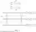
FIG. 1 is a diagram illustrating two comparators 101 and 102 configured to determine states of a differential input signal (e.g. a difference between a pair of differential input signals, which is referred to as an input signal DIN for brevity) of a three-level pulse-amplitude modulation (PAM3) circuit according to an embodiment of the present invention, where the comparator 101 is configured to determine whether the input signal DIN is greater than a threshold VTHH to generate output signals {VCH, VCHB}, and the comparator 102 is configured to determine whether the input signal DIN is less than the threshold VTHL to generate output signals {VCL, VCLB}, where the threshold VTHH is greater than the threshold VTHL. In this embodiment, when the input signal DIN falls in an interval greater than the threshold VTHH, the comparator 101 may determine that the input signal DIN is greater than the threshold VTHH and the comparator 102 may determine that the input signal DIN is greater than the threshold VTHL, where the output signals {VCH, VCHB} generated by the comparator 101 is {1, 0} and the output signals {VCL, VCLB} generated by the comparator 102 is {1, 0}, which indicate that the input signal DIN is at a high level state (which is referred to as a HIGH state for brevity). When the input signal DIN falls in an interval which is less than the threshold VTHH but greater than the threshold VTHL, the comparator 101 may determine that the input signal DIN is less than the threshold VTHH and the comparator 102 may determine that the input signal DIN is greater than the threshold VTHL, where the output signals {VCH, VCHB} generated by the comparator 101 is {0, 1} and the output signals {VCL, VCLB} generated by the comparator 102 is {1, 0}, which indicate that the input signal DIN is at a middle level state (which is referred to as a MID state for brevity). When the input signal DIN falls in an interval less than the threshold VTHL, the comparator 101 may determine that the input signal DIN is less than the threshold VTHH and the comparator 102 may determine that the input signal DIN is less than the threshold VTHL, where the output signals {VCH, VCHB} generated by the comparator 101 are {0, 1} and the output signals {VCH, VCLB} generated by the comparator 102 are {0, 1}, which indicate that the input signal DIN is at a low level state (which is referred to as a LOW state).
FIG. 2 is a diagram illustrating a behavior model of a decision feedback equalizer (DFE) 20 within the PAM3 circuit according to an embodiment of the present invention. As shown in FIG. 2, the DFE 20 may comprise the comparators 101 and 102 and a calculating circuit such as a summation circuit 110, where the summation circuit 110 is coupled to the comparators 101 and 102. It should be noted that signals involved in operations of the DFE 20 shown in FIG. 2 may be differential signals, and these differential signals are illustrated by single-ended signals (e.g. a difference between each pair of differential signals) for brevity, as shown by an input signal IN, a calculation signal such as a summation signal OUT, output signals RH and RL, and delayed signals RDH1, RDL1, RDH2 and RDL2. For example, the output signal Ru may represent a difference between the output signals {VCH, VCHB} (e.g. RH=VCH−VCHB), and the output signal RL may represent a difference between the output signals {VCL, VCLB} (e.g. RL=VCL−VCLB). In this embodiment, the comparator 101 is configured to compare the summation signal OUT with the threshold VTHH to generate a comparison result such as the output signal RH, and the comparator 102 is configured to compare the summation signal OUT with the threshold VTHL to generate a comparison result such as the output signal RL, where the summation circuit 110 is configured to generate the summation signal OUT according to the input signal IN, a delayed signal (e.g. RDH1 and RDH2) of the output signal RH, and a delayed signal (e.g. RDL1 and RDL2) of the output signal RL. In particular, the summation circuit 110 may perform calculation (e.g. summation) on the input signal IN and the delayed signal RDH1, RDH2, RDL1 and RDL2 to generate the summation signal OUT, where the delayed signal RDH1 is generated by applying a first predetermined delay (e.g. Td1) to the output signal RH and multiplying by a first predetermined coefficient (e.g. h1), the delayed signal RDH2 is generated by applying a second predetermined delay (e.g. Td1+Td2) to the output signal RH and multiplying by a second predetermined coefficient (e.g. h2), the delayed signal RDL1 is generated by applying the first predetermined delay (e.g. Td1) to the output signal RL and multiplying by the first predetermined coefficient (e.g. h1), and the delayed signal RDL2 is generated by applying the second predetermined delay (e.g. Td1+Td2) to the output signal RL and multiplying by the second predetermined coefficient (e.g. h2).
It should be noted that, when the summation signal OUT is at the MID state in a certain cycle of a clock signal CLK, the output signals RH and RL generated in this cycle are unable to have decision feedback equalization effects on the input signal IN (e.g. feedbacks of the output signal RH and RL may cancel each other), which makes an effect of the decision feedback equalization provided by the DFE 20 insufficient. Furthermore, in some designs, functions of the summation circuit 110 may be integrated into input stages of the comparators 101 and 102. FIG. 3 is a diagram illustrating a behavior model of a DFE 30 within the PAM3 circuit which utilizes comparators with summation functions according to an embodiment of the present invention. The DFE 30 may comprise comparators 121 and 122 which are equipped with calculation functions such as summation functions, where the comparator 121 may comprise a calculating circuit such as a summation circuit 111 and the comparator 101, and the comparator 122 may comprise a calculating circuit such as a summation circuit 112 and the comparator 102. In particular, the summation circuit 111 is configured to execute operations of the summation circuit 110 shown by FIG. 2 in the comparator 121 to generate the summation signal OUT1, and the summation circuit 112 is configured to execute operations of the summation circuit 110 shown by FIG. 2 in the comparator 122 to generate the summation signal OUT2. As shown in FIG. 3, both the comparators 121 and 122 need to receive the delayed signal RDH1, RDH2, RDL1 and RDL2, and overall wirings therefore become quite complicated. This makes it difficult to simplify the DFE 20 by integrating a summing operation and a comparing operation into a single circuit.
FIG. 4 is a diagram illustrating a behavior model of a DFE 40 within the PAM3 circuit according to an embodiment of the present invention. As shown in FIG. 4, the DFE 40 may comprise the comparator 101, a first calculating circuit such as the summation circuit 111, the comparator 102 and a second calculating circuit such as the summation circuit 112, where the summation circuit 111 is coupled to the comparator 101, and the summation circuit 112 is coupled to the comparator 102. In this embodiment, the comparator 101 is configured to compare a first calculation signal such as a summation signal OUTH with the threshold VTHH to generate a first comparison result such as the output signal RH, and the summation circuit 111 is configured to generate the summation signal OUTH according to the input signal IN and a first delayed signal (e.g. the delayed signal RDH1 and RDH2) of the output signal RH. In addition, the comparator 102 is configured to compare a second calculation signal such as a summation signal OUTL with the threshold VTHL to generate a second comparison result such as the output signal RL, and the summation circuit 112 is configured to generate the summation signal OUTL according to the input signal IN and a second delayed signal (e.g. the delayed signal RDL1 and RDL2) of the output signal RL.
Similar to the embodiment of FIG. 2, the delayed signal RDH1 is generated by applying the first predetermined delay (e.g. Td1) to the output signal Ru and multiplying by the first predetermined coefficient (e.g. h1), the delayed signal RDH2 is generated by applying the second predetermined delay (e.g. Td1+Td2) to the output signal RH and multiplying by the second predetermined coefficient (e.g. h2), the delayed signal RDL1 is generated by applying the first predetermined delay (e.g. Td1) to the output signal RI, and multiplying by the first predetermined coefficient (e.g. h1), and the delayed signal RDL2 is generated by applying the second predetermined delay (e.g. Td1+Td2) to the output signal RL and multiplying by the second predetermined coefficient (e.g. h2). It should be noted that, in this embodiment, the summation circuit 111 is configured to perform calculation (e.g. summation) on the input signal IN and the first delayed signal (e.g. the delayed signal RDH1 and RDH2 to generate the summation signal OUTH. As the summation circuit 111 will not receive the second delayed signal (e.g. the delayed signal RDL1 and RDL2), the summation signal OUTH output by the summation circuit 111 is related to the input signal IN and the output signal RH only (i.e. related to the delayed signal RDH1 and RDL2), and is unrelated to the output signal RL (i.e. unrelated to the delayed signal RDL1 and RDL2). In addition, the summation circuit 112 is configured to perform calculation (e.g. summation) on the input signal IN and the second delayed signal (e.g. the delayed signal RDL1 and RDL2) to generate the summation signal OUTL. As the summation circuit 112 will not receive the first delayed signal (e.g. the delayed signal RDH1 and RDH2), the summation signal OUTL output by the summation circuit 112 is related to the input signal IN and the output signal RL (i.e. related to the delayed signal RDL1 and RDL2) only, and is unrelated to the output signal RH (i.e. unrelated to the delayed signal RDH1 and RDH2).
In this embodiment, operations of the summation circuit 111 and the comparator 101 may be integrated into the comparator 121 equipped with the calculation function such as the summation function, and operations of the summation circuit 112 and the comparator 102 may be integrated into the comparator 122 equipped with the calculation function such as the summation function. In comparison with the DFE 20 shown in FIG. 2, the DFE 40 shown in FIG. 4 is more favorable to the purpose of integrating the summation operation and the comparing operation into a single circuit for circuit simplification.
FIG. 5 is a diagram illustrating the DFE 40 shown in FIG. 4 in another aspect. As shown in FIG. 5, an output of the comparator 121 (i.e. the output signal RH) may be fed back to an input of the comparator 121 (e.g. an input of the summation circuit 111) only, and an output of the comparator 122 (i.e. the output signal RL) may be fed back to an input of the comparator 122 (e.g. an input of the summation circuit 112) only. Thus, the comparators 121 and 122 have respective independent decision feedback equalization loops and will not affect each other. Even if the summation signal OUTH or OUTL is at the MID state (e.g. falls in the interval which is less than the threshold VTHH but higher than VTHL), each of the comparators 121 and 122 can still perform the decision feedback equalization on the input signal IN. For example, the summation signal OUTH generated by the summation circuit 111 may have a better upper eye diagram due to the decision feedback equalization performed by the comparator 121, and the summation signal OUTL generated by the summation circuit 112 may have a better lower eye diagram due to the decision feedback equalization performed by the comparator 122. It should be noted that the number of taps of the DFE 40 is not limited to that of the architecture shown in FIG. 4 or FIG. 5. In some embodiment, the number of taps of the DFE 40 may vary, and architectures with different numbers of taps may be deduced by analogy.
In the decision feedback equalization loop of the comparator 121, when the summation signal OUTH is greater than the threshold VTHH, the summation circuit 111 may decrease the summation signal OUTH according to a first logic state of the output signal RH (e.g. {VCH, VCHB}={1, 0}), and when the summation signal OUTH is less than the threshold VTHH, the summation circuit 111 may increase the summation signal OUTH according to a second logic state of the output signal RH (e.g. {VCH, VCHB}={0, 1}). In the decision feedback equalization loop of the comparator 122, when the summation signal OUTL is greater than the threshold VTHL, the summation circuit 112 may decrease the summation signal OUTL according to a first logic state of the output signal RL (e.g. {VCL, VCLB}={1, 0}), and when the summation signal OUTL is less than the threshold VTHL, the summation circuit 112 may increase the summation signal OUTL according to a second logic state of the output signal RL (e.g. {VCL, VCLB}={0, 1}).
FIG. 6 is a diagram illustrating circuit implementation of the DFE 40 shown in FIG. 5 according to an embodiment of the present invention. As shown in FIG. 6, the summation circuit 111 of the DFE 40 may comprise at least one first transistor (e.g. transistors MH1 and MH2) and at least one second transistor (e.g. transistors MH3 and MH4), where drain terminals of the transistors MH1 and MH2 and drain terminals of the transistor MH3 and MH4 are coupled to input terminals of the comparator 101. In this embodiment, the at least one first transistor (e.g. the transistors MH1 and MH2) is configured to receive the input signal IN (e.g. the transistor MH1 is configured to receive an input signal VIP and the transistor MH2 is configured to receive an input signal VIN), where the input signal IN may represent a difference between the input signals {VIP, VIN} (e.g. IN=VIP−VIN). The at least one second transistor (e.g. the transistors MH3 and MH4) is configured to receive the first comparison result such as the output signal RH (e.g. the transistor MH3 is configured to receive the output signal VCH and the transistor MH4 is configured to receive the output signal VCHB), where the output signal Ru may represent a difference between the output signals {VCH, VCHB} (e.g. RH=VCH−VCHB). More particularly, the at least one first transistor (e.g. the transistors MH1 and MH2) and the at least one second transistor (e.g. the transistors MH3 and MH4) perform current summation on the input terminals of the comparator 101 to generate the summation signal OUTH (e.g. generating a summation signal VOHP on the drain terminals of the transistor MH1 and MH2 and generating a summation signal VOHP on the drain terminals of the transistor MH2 and MH4), where the summation signal OUTH may represent a difference between the summation signals {VOHP, VOHN} (e.g. OUTH=VOHP−VOHN). In addition, the summation circuit 112 of the DFE 40 may comprise at least one third transistor (e.g. transistors ML1 and ML2) and at least one fourth transistor (e.g. transistors ML3 and ML4), where drain terminals of the transistors ML1 and ML2 and drain terminals of the transistor ML3 and ML4 are coupled to input terminals of the comparator 102. In this embodiment, the at least one third transistor (e.g. the transistor ML1 and ML2) is configured to receive the input signal IN (e.g. the transistor Mui is configured to receive the input signal VIP and the transistor ML2 is configured to receive the input signal VIN). The at least one fourth transistor (e.g. the transistor ML3 and ML4) is configured to receive the second comparison result such as the output signal RL (e.g. the transistor ML3 is configured to receive the output signal VCL and the transistor ML4 is configured to receive the output signal VCLB), where the output signal RL may represent a difference between the output signals {VCL, VCLB} (e.g. RL=VCL−VCLB). More particularly, the at least one third transistor (e.g. the transistors ML1 and ML2) and the at least one fourth transistor (e.g. the transistors ML3 and ML4) perform current summation on the input terminals of the comparator 102 to generate the summation signal OUTL (e.g. generating a summation signal VOLP on the drain terminals of the transistors ML1 and ML3 and generating a summation signal VOLN on the drain terminal of the transistors ML2 and ML4), where the summation signal OUTL may represent a difference between the summation signals {VOLP, VOLN} (e.g. OUTL=VOLP−VOLN).
In particular, the drain terminals of the transistors MH1 and MH3 are coupled to a resistor RHP, and the drain terminals of the transistor MH2 and MH4 are coupled to a resistor RHN, where source terminals of the transistors MH1 and MH2 are coupled to a current source I1MAIN, and source terminals of the transistors MH3 and MH4 are coupled to a current source I1TAP. Thus, the input signals VIP and VIN may control a ratio of currents flowing to the resistors RHP and RHN from the current source I1MAN, and the output signal VCH and VCHB may control a ratio of currents flowing to the resistors RHP and RHN from the current source I1TAP. In addition, the drain terminals of the transistors ML1 and ML3 are coupled to a resistor RLP, and the drain terminals of the transistor ML2 and ML4 are coupled to a resistor RLN, where source terminals of the transistors ML1 and ML2 are coupled to the current source I2MAIN, and source terminals of the transistors ML3 and ML4 are coupled to the current source I2TAP. Thus, the input signals VIP and VIN may control a ratio of currents flowing to the resistor RLP and RLN from the current source I2MAIN, and the output signals VCL and VCLB may control a ratio of currents flowing to the resistors RLP and RLN from the current source I2TAP.
In addition, the predetermined delay Td1 shown in FIG. 5 may be implemented by controlling timing of transmitting the output signals VCH and VCHB to gate terminals of the transistors MH3 and MH4 based on the clock signal CLK (or controlling timing of transmitting the output signals VCL and VCLB to gate terminals of the transistors ML3 and ML4), and the predetermined coefficient h1 shown in FIG. 5 may be determined by a ratio of the current of the current source I1MAIN and the current of the current source I1TAP (or a ratio of the current of the current source I2MAIN and the current of the current source I2TAP), but the present invention is not limited thereto. It should be noted that FIG. 6 merely shows the implementation of one-tap architecture, and more particularly, merely shows the implementation of performing the decision feedback equalization based on the delayed signals RDH1 and RDL1, where the implementation of performing the decision feedback equalization based on the delayed signals RDH2 and RDH2 is omitted in FIG. 6 for brevity, and those skilled in this art should be able to deduce by analogy how to implement multi-tap architecture (e.g. 1.5-tap architecture which may be referred to as TAP-1.5, two-tap architecture which may be referred to as TAP-2) according to the one-tap architecture shown in FIG. 6.
As mentioned above, the at least one second transistor may comprise the transistors MH3 and MH4, and the summation signal OUTH shown in FIG. 5 may represent a difference between a first positive calculation signal (e.g. the summation signal VOHP) on the drain terminal of the transistor MH3 and a first negative calculation signal (e.g. the summation signal VOHN) on the drain terminal of the transistor MH4, such as the summation signal OUTH (e.g. OUTH=VOHP−VOHN). When the difference such as the summation signal OUTH is greater than the threshold VTHH, the transistor MH4 may be turned on (e.g. conductive) in response to a first logic state of the output signals {VCH, VCHB} (e.g. {VCH, VCHB}={1, 0}) and the transistor Mus may be turned off (e.g. non-conductive) in response to {VCH, VCHB}={1, 0}), in order to add a unit feedback signal (e.g. a feedback signal corresponding to the current of the current source I1TAP) to the summation signal VOHN for decreasing the first calculation signal such as the summation signal OUTH (e.g. decreasing (VOHP−VOHN)). When the difference such as the summation signal OUTH is less than the threshold VTHH, the transistor MH3 may be turned on in response to a second logic state of the output signals {VCH, VCHB} (e.g. {VCH, VCHB}={0, 1}) and the transistor MH4 may be turned off in response to {VCH, VCHB}={0, 1}, in order to add the unit feedback signal (e.g. the feedback signal corresponding to the current of the current source I1TAP) to the summation signal VOHP, for increasing the first calculation signal such as the summation signal OUTH (e.g. increasing (VOHP−VOHN)).
In addition, the at least one fourth transistor may comprise the transistors ML3 and ML4, and the summation signal OUTL shown in FIG. 5 may represent a difference between a second positive calculation signal (e.g. the summation signal VOLP) on the drain terminal of the transistor ML3 and a second negative calculation signal (e.g. the summation signal VOLN) on the drain terminal of the transistor ML4, such as the summation signal OUTL (e.g. OUTL=VOLP−VOLN). When the difference such as the summation signal OUTL is greater than the threshold VTHL, the transistor ML4 may be turned on in response to a first logic state of the output signals {VCL, VCLB} (e.g. {VCL, VCLB}={1, 0}) and the transistor ML3 may be turned off in response to {VCL, VCLB}={1, 0}, in order to add a unit feedback signal (e.g. a feedback signal corresponding to the current of the current source I2TAP) to the summation signal VOLN for decreasing the second calculation signal such as the summation signal OUTL (e.g. decreasing (VOLP−VOLN)). When the difference such as the summation signal OUTL is less than the threshold VTHL, the transistor ML3 may be turned on in response to a second logic state of the output signals {VCL, VCLB} (e.g. {VCL, VCLB}={0, 1} and the transistor ML4 may be turned off in response to {VCL, VCLB}={0, 1}, in order to add the unit feedback signal (e.g. the feedback signal corresponding to the current of the current source I2TAP) to the summation signal VOLP for increasing the second calculation signal such as the summation signal OUTL (e.g. increasing (VOLP−VOLN)).
It should be noted that the DFE 40 provided by the embodiment of the present invention is applied to the PAM3 circuit as an example, but the present invention is not limited thereto. For example, a DFE applied to a PAM4 circuit may be implemented by modifying the number of comparators and the number of decision feedback equalization loops within the DFE 40, and related details are omitted here for brevity. In addition, feedback operations of the feedback signals (e.g. the delayed signal RDH1, RDH2, RDL1 and RDL2) performed on the summation signal OUTH and OUTL by the summation circuits 111 and 112 may be summation or subtraction. In addition, the summation circuits 111 and 112 of the present invention are not limited to implementation of current mode logics (CMLs) with P-type transistor inputs. In some embodiment, the summation circuits 111 and 112 may be implemented by CMLs with N-type transistor inputs. In addition, loop architectures of the DFE 20 and the DFE 40 may be combined. In addition, a relationship between a data rate and a clock rate of the DFE 40 is not limited to specific ratios. For example, the DFE 40 may be a full-rate DFE, a half-rate DFE or a quarter-rate DFE.
FIG. 7 is a diagram illustrating a working flow of a method for performing decision feedback equalization on an input signal in a DFE (e.g. the DFE 40 shown in FIG. 4 or FIG. 5) according to an embodiment of the present invention. It should be noted that the working flow shown in FIG. 7 is for illustrative purposes only, and is not meant to be a limitation of the present invention. For example, one or more steps may be added, deleted or modified in the working flow shown in FIG. 7. In addition, if a same result may be obtained, these steps do not have to be executed in the exact order shown in FIG. 7.
In Step S710, the DFE may utilize a first comparator therein to compare a first calculation signal with a first threshold to generate a first comparison result, wherein the first calculation signal is generated according to the input signal and a first delayed signal of the first comparison result by a first calculating circuit of the DFE.
In Step S720, the DFE may utilize a second comparator therein to compare a second calculation signal with a second threshold to generate a second comparison result, wherein the second calculation signal is generated according to the input signal and a second delayed signal of the second comparison result by a second calculating circuit of the DFE.
To summarize, the DFE 40 provided by the embodiments of the present invention makes each decision feedback equalization loop composed of a comparator and a calculation circuit (e.g. a summation circuit) independent of each other, thereby ensuring that each decision feedback equalization loop can introduce its own decision feedback equalization effect. In addition, in the architecture where these decision feedback equalization loops are independent of each other, when the summation circuit is integrated into the comparator, the wiring complexity of the circuit layout will not be greatly increased, which is more conducive to the simplification of the overall circuit. Thus, the present invention can solve the problems of the related art without introducing any side effect or in a way that is less likely to introduce side effects.
Those skilled in the art will readily observe that numerous modifications and alterations of the device and method may be made while retaining the teachings of the invention. Accordingly, the above disclosure should be construed as limited only by the metes and bounds of the appended claims.
Claims
What is claimed is:1. A decision feedback equalizer (DFE), comprising:
a first comparator, configured to compare a first calculation signal with a first threshold to generate a first comparison result;
a first calculating circuit, coupled to the first comparator, configured to generate the first calculation signal according to an input signal and a first delayed signal of the first comparison result;
a second comparator, configured to compare a second calculation signal with a second threshold to generate a second comparison result; and
a second calculating circuit, coupled to the second comparator, configured to generate the second calculation signal according to the input signal and a second delayed signal of the second comparison result.
2. The DFE of claim 1, wherein the first calculating circuit is configured to perform calculation on the input signal and the first delayed signal to generate the first calculation signal, and the second calculating circuit is configured to perform calculation on the input signal and the second delayed signal to generate the second calculation signal.
3. The DFE of claim 1, wherein the first delayed signal is generated by applying a predetermined delay to the first comparison result and multiplying by a predetermined coefficient, and the second delayed signal is generated by applying the predetermined delay to the second comparison result and multiplying by the predetermined coefficient.
4. The DFE of claim 1, wherein:
when the first calculation signal is greater than the first threshold, the first calculating circuit decreases the first calculation signal according to a first logic state of the first comparison result; and
when the first calculation signal is less than the first threshold, the first calculating circuit increases the first calculation signal according to a second logic state of the first comparison result.
5. The DFE of claim 1, wherein:
when the second calculation signal is greater than the second threshold, the second calculating circuit decreases the second calculation signal according to a first logic state of the second comparison result; and
when the second calculation signal is less than the second threshold, the second calculating circuit increases the second calculation signal according to a second logic state of the second comparison result.
6. The DFE of claim 1, wherein:
the first calculating circuit comprises:
at least one first transistor, configured to receive the input signal, wherein a drain terminal of the at least one first transistor is coupled to an input terminal of the first comparator; and
at least one second transistor, configured to receive the first comparison result, wherein a drain terminal of the at least one second transistor is coupled to the input terminal of the first comparator;
wherein the at least one first transistor and the at least one second transistor perform current summation to generate the first calculation signal on the input terminal of the first comparator; and
the second calculating circuit comprises:
at least one third transistor, configured to receive the input signal, wherein a drain terminal of the at least one third transistor is coupled to an input terminal of the second comparator; and
at least one fourth transistor, configured to receive the second comparison result, wherein a drain terminal of the at least one fourth transistor is coupled to the input terminal of the second comparator;
wherein the at least one third transistor and the at least one fourth transistor perform current summation to generate the second calculation signal on the input terminal of the second comparator.
7. The DFE of claim 6, wherein:
the at least one second transistor comprises a second positive transistor and a second negative transistor, and the first calculation signal represents a difference between a first positive calculation signal on a drain terminal of the second positive transistor and a first negative calculation signal on a drain terminal of the second negative transistor;
when the difference is greater than the first threshold, the second negative transistor is turned on in response to a first logic state of the first comparison result to add a unit feedback signal to the first negative calculation signal for decreasing the first calculation signal; and
when the difference is less than the first threshold, the second positive transistor is turned on in response to a second logic state of the first comparison result to add the unit feedback signal to the first positive calculation signal for increasing the first calculation signal.
8. The DFE of claim 6, wherein:
the at least one fourth transistor comprises a fourth positive transistor and a fourth negative transistor, and the second calculation signal represents a difference between a second positive calculation signal on a drain terminal of the fourth positive transistor and a second negative calculation signal on a drain terminal of the fourth negative transistor;
when the difference is greater than the second threshold, the fourth negative transistor is turned on in response to a first logic state of the second comparison result to add a unit feedback signal to the second negative calculation signal for decreasing the second calculation signal; and
when the difference is less than the second threshold, the fourth positive transistor is turned on in response to a second logic state of the second comparison result to add the unit feedback signal to the second positive calculation signal for increasing the second calculation signal.
9. A method for performing decision feedback equalization on an input signal in a decision feedback equalizer (DFE), comprising:
utilizing a first comparator of the DFE to compare a first calculation signal with a first threshold to generate a first comparison result, wherein the first calculation signal is generated according to the input signal and a first delayed signal of the first comparison result by a first calculating circuit of the DFE; and
utilizing a second comparator of the DFE to compare a second calculation signal with a second threshold to generate a second comparison result, wherein the second calculation signal is generated according to the input signal and a second delayed signal of the second comparison result by a second calculating circuit of the DFE.
10. The method of claim 9, wherein the first calculation signal is generated by performing calculation on the input signal and the first delayed signal, and the second calculation signal is generated by performing calculation on the input signal and the second delayed signal.
11. The method of claim 9, wherein the first delayed signal is generated by applying a predetermined delay to the first comparison result and multiplying by a predetermined coefficient, and the second delayed signal is generated by applying the predetermined delay to the second comparison result and multiplying by the predetermined coefficient.
12. The method of claim 9, further comprising:
in response to the first calculation signal being greater than the first threshold, utilizing the first calculating circuit to decrease the first calculation signal according to a first logic state of the first comparison result.
13. The method of claim 9, further comprising:
in response to the first calculation signal being less than the first threshold, utilizing the first calculating circuit to increase the first calculation signal according to a second logic state of the first comparison result.
14. The method of claim 9, further comprising:
in response to the second calculation signal being greater than the second threshold, utilizing the second calculating circuit to decrease the second calculation signal according to a first logic state of the second comparison result.
15. The method of claim 9, further comprising:
in response to the second calculation signal being less than the second threshold, utilizing the second calculating circuit to increase the second calculation signal according to a second logic state of the second comparison result.
16. The method of claim 9, further comprising:
utilizing at least one first transistor of the first calculating circuit to receive the input signal, wherein a drain terminal of the at least one first transistor is coupled to an input terminal of the first comparator;
utilizing at least one second transistor of the first calculating circuit to receive the first comparison result, wherein a drain terminal of the at least one second transistor is coupled to the input terminal of the first comparator;
utilizing the at least one first transistor and the at least one second transistor to perform current summation to generate the first calculation signal on the input terminal of the first comparator;
utilizing at least one third transistor of the second calculating circuit to receive the input signal, wherein a drain terminal of the at least one third transistor is coupled to an input terminal of the second comparator;
utilizing at least one fourth transistor of the second calculating circuit to receive the second comparison result, wherein a drain terminal of the at least one fourth transistor is coupled to the input terminal of the second comparator; and
utilizing the at least one third transistor and the at least one fourth transistor to perform current summation to generate the second calculation signal on the input terminal of the second comparator.
17. The method of claim 16, wherein the at least one second transistor comprises a second positive transistor and a second negative transistor, the first calculation signal represents a difference between a first positive calculation signal on a drain terminal of the second positive transistor and a first negative calculation signal on a drain terminal of the second negative transistor, and the method further comprises:
in response to the difference being greater than the first threshold, turning on the second negative transistor in response to a first logic state of the first comparison result to add a unit feedback signal to the first negative calculation signal for decreasing the first calculation signal.
18. The method of claim 16, wherein the at least one second transistor comprises a second positive transistor and a second negative transistor, the first calculation signal represents a difference between a first positive calculation signal on a drain terminal of the second positive transistor and a first negative calculation signal on a drain terminal of the second negative transistor, and the method further comprises:
in response to the difference being less than the first threshold, turning on the second positive transistor in response to a second logic state of the first comparison result to add the unit feedback signal to the first positive calculation signal for increasing the first calculation signal.
19. The method of claim 16, wherein the at least one fourth transistor comprises a fourth positive transistor and a fourth negative transistor, the second calculation signal represents a difference between a second positive calculation signal on a drain terminal of the fourth positive transistor and a second negative calculation signal on a drain terminal of the fourth negative transistor, and the method further comprises:
in response to the difference being greater than the second threshold, turning on the fourth negative transistor in response to a first logic state of the second comparison result to add a unit feedback signal to the second negative calculation signal for decreasing the second calculation signal.
20. The method of claim 16, wherein the at least one fourth transistor comprises a fourth positive transistor and a fourth negative transistor, the second calculation signal represents a difference between a second positive calculation signal on a drain terminal of the fourth positive transistor and a second negative calculation signal on a drain terminal of the fourth negative transistor, and the method further comprises:
in response to the difference being less than the second threshold, turning on the fourth positive transistor in response to a second logic state of the second comparison result to add the unit feedback signal to the second positive calculation signal for increasing the second calculation signal.
Images & Drawings included:


Sources:
- United States Patent and Trademark Office - verify current appl. status at the USPTO↗
Recent applications in this class:
- » 20260058849 2026-02-26
CONTINUOUS TIME LINEAR EQUALIZER EMPLOYING CURRENT-REUSE AND CURRENT-STEALING ARCHITECTURE - » 20250293903 2025-09-18
Systems and Methods for Low Latency Transmission and Digital Link Adaptation - » 20250260604 2025-08-14
FEED FORWARD EQUALIZERS WITH CURRENT MODE SAMPLING - » 20250233781 2025-07-17
WIDE DYNAMIC RANGE CONTINUOUS-TIME LINEAR EQUALIZER (CTLE) - » 20250193058 2025-06-12
COMMUNICATION APPARATUS, LEARNING APPARATUS, COMMUNICATION SYSTEM, CONTROL CIRCUIT, STORAGE MEDIUM, AND STEP SIZE UPDATE METHOD - » 20250097083 2025-03-20
PROGRAMMABLE EQUALIZER - » 20240414032 2024-12-12
EQUALIZATION TRAINING METHOD AND APPARATUS, AND SYSTEM - » 20240283679 2024-08-22
Continuous time linear equalizer of single-ended signal with input coupling capacitor - » 20240259238 2024-08-01
PASSIVE EQUALIZER - » 20240195663 2024-06-13
Clock and data recovery circuit and feed forward equalizer decoupling
Recent applications for this Assignee:
- » 20260088833 2026-03-26
METHOD FOR PERFORMING PARITY BIT CALCULATION WITH AID OF CIRCUIT COMPLEXITY REDUCTION FOR PERFORMING ERROR CORRECTION, AND ASSOCIATED APPARATUS - » 20260088775 2026-03-26
LINEAR AMPLIFYING DEVICE AND LINEAR AMPLIFYING METHOD THEREOF - » 20260086145 2026-03-26
CHIP, SYSTEM, AND METHOD FOR BOUNDARY TESTING - » 20260082061 2026-03-19
TRANSMISSION BANDWIDTH ALLOCATION METHOD AND COMMUNICATION DEVICE - » 20260081639 2026-03-19
INFORMATION TRANSCEIVING METHOD AND ASSOCIATED COMMUNICATION DEVICES - » 20260080546 2026-03-19
IMAGE PROCESSING METHOD AND ASSOCIATED IMAGE PROCESSING CIRCUIT - » 20260075395 2026-03-12
PROVISIONING METHOD AND DEVICE FOR BLUETOOTH MESH NETWORK - » 20260074690 2026-03-12
SIGNAL TRANSMISSION INTERFACE - » 20260073891 2026-03-12
METHOD FOR PERFORMING CONSUMER ELECTRONICS CONTROL COMMUNICATION WITH REMOTE DEVICE HAVING HIGH-DEFINITION MULTIMEDIA INTERFACE PORT WITH AID OF MULTIPLE VIRTUAL NETWORK BLOCKS, AND ASSOCIATED APPARATUS - » 20260067561 2026-03-05
OCCLUSION JUDGMENT SYSTEM, OCCLUSION JUDGMENT METHOD, COMPUTER READABLE RECORDING MEDIUM WITH STORED PROGRAM, AND NON-TRANSITORY COMPUTER PROGRAM PRODUCT