NANOPARTICLE, AND INK COMPOSITION, LIGHT-EMITTING DEVICE, ELECTRONIC APPARATUS AND ELECTRONIC DEVICE, INCLUDING THE NANOPARTICLE
US20260132052A1
2026-05-14
19/384,354
2025-11-10
Smart Summary: Nanoparticles are tiny particles made from metal oxides and have special surface attachments called ligands. These ligands contain a carboxyl group, which helps the nanoparticles work better. The nanoparticles can be used in various applications, including inks for printing and light-emitting devices. They are also useful in electronic devices and other electronic equipment. Overall, these nanoparticles enhance the performance of technology by improving light emission and conductivity. 🚀 TL;DR
Abstract:
Nanoparticles, and an ink composition, a light-emitting device, an electronic apparatus, and an electronic device, including the nanoparticles are provided. Each of the nanoparticles include a metal oxide nanoparticle represented by Formula 1 and a ligand on the surface of the metal oxide nanoparticle, and the ligand includes a carboxyl group:
-
- wherein, in Formula 1, 0<x<1 and M includes at least one metal element.
Inventors:
- Myoungjin PARK 18 🇰🇷 Yongin-si, South Korea
- Jaehoon Lim 2 🇰🇷 Seongnam-si, South Korea
- Yeongho Choi 2 🇰🇷 Seongnam-si, South Korea
- Woon Ho Jung 1 🇰🇷 Suwon-si, South Korea
Applicant:
Interested in similar patents?
Get notified when new applications in this technology area are published.
Classification:
C01G53/66 » CPC main
Compounds of nickel; Nickelates containing alkaline earth metals, e.g. SrNiO, SrNiO
C09K11/883 » CPC further
Luminescent, e.g. electroluminescent, chemiluminescent materials containing inorganic luminescent materials containing selenium, tellurium or unspecified chalcogen elements; Chalcogenides with zinc or cadmium
C09K11/88 IPC
Luminescent, e.g. electroluminescent, chemiluminescent materials containing inorganic luminescent materials containing selenium, tellurium or unspecified chalcogen elements
Description
CROSS-REFERENCE TO RELATED APPLICATION
This application claims priority to and benefit of Korean Patent Application No. 10-2024-0160487, filed on Nov. 12, 2024, in the Korean Intellectual Property Office, the entire disclosure of which is incorporated herein by reference.
BACKGROUND
1. Field
One or more aspects of embodiments of the present disclosure relate to nanoparticles, and an ink composition, a light-emitting device, an electronic apparatus and an electronic device, including the nanoparticles.
2. Description of the Related Art
From among light-emitting devices, self-emissive devices have relatively wide viewing angles, high contrast ratios, short response times, and excellent or suitable characteristics in terms of luminance, driving voltage, and response speed.
In a light-emitting device, a first electrode is on a substrate, and a hole transport region, an emission layer, an electron transport region, and a second electrode are sequentially on the first electrode. Holes provided from the first electrode move toward the emission layer through the hole transport region, and electrons provided from the second electrode move toward the emission layer through the electron transport region. Carriers, such as holes and electrons, recombine in the emission layer to produce excitons. The excitons may transition (e.g., relax) from an excited state to a ground state, thereby generating light.
SUMMARY
One or more aspects of embodiments of the present disclosure are directed toward nanoparticles, and an ink composition, a light-emitting device, an electronic apparatus, and an electronic device, including the nanoparticles.
However, it should be noted that these objectives are merely examples, and the scope of the disclosure is not limited to the herein-mentioned aspects. Rather, additional aspects will be set forth in part in the description which follows and, in part, will be apparent from the description, or may be learned by practice of the presented embodiments of the disclosure.
According to one or more embodiments of the present disclosure, a nanoparticle includes
-
- a metal oxide nanoparticle represented by Formula 1, and
- a ligand on a surface of the metal oxide nanoparticle,
- wherein the ligand includes a carboxyl group:
-
- wherein, in Formula 1, 0<x<1 and M includes at least one metal element.
According to one or more embodiments, an ink composition includes the nanoparticle and at least one solvent.
According to one or more embodiments, a light-emitting device includes
-
- a first electrode,
- a second electrode opposite to (e.g., facing) the first electrode, and
- an interlayer between the first electrode and the second electrode and including an emission layer,
- wherein the interlayer further includes a hole transport region between the first electrode and the emission layer,
- the hole transport region includes the nanoparticles,
- the nanoparticles each include a metal oxide nanoparticle represented by Formula 1, and
- a ligand on the surface of the metal oxide nanoparticle, and
- the ligand includes a carboxyl group:
-
- wherein, in Formula 1, 0<x<1 and M includes at least one metal element.
According to one or more embodiments, an electronic apparatus includes the light-emitting device.
According to one or more embodiments, an electronic device includes the light-emitting device.
BRIEF DESCRIPTION OF THE DRAWINGS
The accompanying drawings are included to provide a further understanding of the preceding and other aspects, features, and advantages of one or more embodiments of the disclosure and are incorporated in and constitute a part of this specification. The drawings illustrate example embodiments that will be more apparent from the following description taken in conjunction with the accompanying drawings. In the drawings:
FIG. 1 is a schematic view of the structure of a light-emitting device according to one or more embodiments;
FIG. 2 is a schematic view of the structure of an electronic apparatus according to one or more embodiments;
FIG. 3 is a schematic view of the structure of an electronic apparatus according to another embodiment;
FIGS. 4, 5, 6A, 6B, and 6C are each a schematic view of the structure of an electronic device according to one or more embodiments;
FIG. 7 is a diagram showing the energy levels of the valence bands of nanoparticles in Preparation Example 2, Preparation Example 4, and Comparative Preparation Example 1;
FIG. 8 is a diagram showing the hole mobility of nanoparticles in Preparation Example 2, Preparation Example 4, and Comparative Preparation Example 1;
FIG. 9 is a diagram showing the absolute quantum efficiency of light-emitting devices of Example 1, Example 2, and Comparative Example 1;
FIGS. 10A and 10B are diagrams showing the turn-on voltage and luminance measured in light-emitting devices of Example 1, Example 2, and Comparative Example 1;
FIG. 11 is a diagram showing the maximum external quantum efficiency measured in light-emitting devices of Example 1, Example 2, and Comparative Example 1; and
FIG. 12 is a diagram showing the absorption and emission spectra of quantum dots included in an emission layer of a light-emitting device of Example 1.
DETAILED DESCRIPTION
Reference will now be made in detail to embodiments, examples of which are illustrated in the accompanying drawings, wherein like reference numerals refer to like elements throughout the specification. In this regard, the present embodiments may have different forms and should not be construed as being limited to the descriptions set forth herein. It should be noted that in the following description, only portions useful for understanding an operation according to the disclosure are described, and descriptions of other portions are not included in order not to obscure the subject matter of the disclosure. Accordingly, the embodiments are merely described by referring to the figures, to explain aspects of the present description in enough detail so that those skilled in the art may easily implement the technical spirit of the disclosure to which the disclosure belongs. As used herein, the term “and/or” includes any and all combinations of one or more of the associated listed items. Throughout the disclosure, the expressions “at least one of a, b or c,” “at least any of a, b, and c,” and “at least any selected from a group consisting of a, b, and c” and/or the like indicate only a, only b, only c, both (e.g., simultaneously) a and b, both (e.g., simultaneously) a and c, both (e.g., simultaneously) b and c, all of a, b, and c, or variations thereof (for example, abc, ab, bc, and cc).
Because the disclosure may have diverse modified embodiments, one or more embodiments are illustrated in the drawings and are described in the detailed description. An effect and a characteristic of the disclosure, and a method of accomplishing these will be apparent when referring to one or more embodiments described with reference to the drawings. The disclosure may, however, be embodied in many different forms and should not be construed as limited to the one or more embodiments set forth herein.
It will be understood that although the terms “first,” “second,” and/or the like used herein may be used herein to describe one or more suitable components, these components should not be limited by these terms. These components are only used to distinguish one component from another. Therefore, a first component may refer to a second component within a range without departing from the scope disclosed herein.
An expression used in the singular such as “a,” “an” and “the” encompasses the expression of the plural, unless it has a clearly different meaning in the context.
The terms “consist(ing) of” used herein refers to the existence of only the corresponding component while excluding the possibility that other components are added. For example, the wording “consist of A, B, and C” refers to the existence of only A, B, and C. In this context, “consisting essentially of” indicates that any additional components will not materially affect the chemical, physical, optical or electrical properties of the semiconductor film.
The terms “includes,” “including,” “include,” “comprises,” “comprising,” “comprise,” “having,” “has,” and/or “have” as used herein refer to that a corresponding component is present, and the possibility of adding one or more other components is not excluded. Unless defined otherwise, these terms may refer to both the case of consisting of the corresponding components and the case of further including other components.
It will be understood that when a layer, region, or component is referred to as being “coupled to,” “on,” or “onto” another layer, region, or component in the present specification, it may be directly or indirectly “coupled to” or “on” the other layer, region, or component. For example, for example, intervening layers, regions, or components may be present.
Sizes of elements in the drawings may be exaggerated for convenience of explanation. In embodiments, because sizes and thicknesses of components in the drawings are arbitrarily illustrated for convenience of explanation, the following embodiments are not limited thereto.
The term “may” will be understood to refer to “one or more embodiments of the present disclosure,” some of which include the described element and some of which exclude that element and/or include an alternate element. Similarly, alternative language such as “or” refers to “one or more embodiments of the present disclosure,” each including a corresponding listed item.
Spatially relative terms such as “below”, “lower”, “above”, “on top”, “on the top”, “under”, “on”, and/or the like may be used for descriptive purposes, thereby describing a relationship between one element or feature and another element(s) or feature(s) as shown in the drawings. Spatially relative terms are intended to include other directions in use, in operation, and/or in manufacturing, in addition to the direction depicted in the drawings. For example, when a device shown in the drawing is turned upside down, elements depicted as being positioned “under” other elements or features are positioned in a direction “on” the other elements or features. Therefore, in one or more embodiments, the term “under” may include both directions of on and under. In some embodiments, the device may face in other directions (for example, rotated 90 degrees or in other directions) and thus the spatially relative terms used herein are interpreted according thereto.
The term “interlayer” as used herein refers to a single layer and/or all of multiple layers arranged between the first electrode and the second electrode of the light-emitting device.
Unless otherwise defined, all terms (including chemical, technical and scientific terms) used herein have a same meaning as commonly understood by one of ordinary skill in the art to which the present disclosure belongs. It will be further understood that terms, such as those defined in commonly used dictionaries, should be interpreted as having a meaning that is consistent with their meaning in the context of the relevant art and will not be interpreted in an idealized or overly formal sense unless expressly so defined herein.
When a certain embodiment may be implemented differently, a specific process order may be performed differently from the described order. For example, two consecutively described processes may be performed substantially at the same time or performed in an order opposite to the described order.
Hereinafter, one or more embodiments of the disclosure are described in more detail with reference to the attached drawings.
Nanoparticles
According to one or more embodiments, each of the nanoparticles provided herein is a nanoparticle including:
-
- a metal oxide nanoparticle represented by Formula 1; and
- a ligand on the surface of the metal oxide nanoparticle,
- wherein the ligand includes a carboxyl group:
-
- wherein, in Formula 1, 0<x<1 and M includes at least one metal element.
According to one or more embodiments, in Formula 1, x may satisfy 0<x<0.5.
For example, x may be greater than 0 and less than 0.5, greater than 0 and not more than 0.45, greater than 0 and not more than 0.4, greater than 0 and not more than 0.3, greater than 0 and not more than 0.2, greater than 0 and not more than 0.1, greater than 0 and not more than 0.09, greater than 0 and not more than 0.08, greater than 0 and not more than 0.07, greater than 0 and not more than 0.06, greater than 0 and not more than 0.05, greater than 0 and not more than 0.04, greater than 0 and not more than 0.03, greater than 0 and not more than 0.02, at least 0.01 but less than 0.5, about 0.01 to about 0.45, about 0.01 to about 0.4, about 0.01 to about 0.3, about 0.01 to about 0.2, about 0.01 to about 0.1, about 0.01 to about 0.09, about 0.01 to about 0.08, about 0.01 to about 0.07, about 0.01 to about 0.06, about 0.01 to about 0.05, about 0.01 to about 0.04, about 0.01 to about 0.03, about 0.01 to about 0.02, at least 0.02 but less than 0.5, about 0.02 to about 0.45, about 0.02 to about 0.4, about 0.02 to about 0.3, about 0.02 to about 0.2, about 0.02 to about 0.1, about 0.02 to about 0.09, about 0.02 to about 0.08, about 0.02 to about 0.07, about 0.02 to about 0.06, about 0.02 to about 0.05, about 0.02 to about 0.04, about 0.02 to about 0.03, at least 0.03 but less than 0.5, about 0.03 to about 0.45, about 0.03 to about 0.4, about 0.03 to about 0.3, about 0.03 to about 0.2, about 0.03 to about 0.1, about 0.03 to about 0.09, about 0.03 to about 0.08, about 0.03 to about 0.07, about 0.03 to about 0.06, about 0.03 to about 0.05, or about 0.03 to about 0.04.
According to one or more embodiments, M may include Mg, Zn, Sn, Cu, Pb, Al, In, Sr, Pd, Cd, Ag, or any combination thereof.
For example, M may include Mg, Zn, Sn, or any combination thereof.
For example, M may be Mg.
According to one or more embodiments, the metal oxide nanoparticle may have an alloy structure including (e.g., consisting of) Ni, M, and O. For example, the metal oxide nanoparticle may have a structure in which Ni, M, and O are evenly distributed. Alternatively, the metal oxide nanoparticle may have a structure in which Ni and O form a core and M is bound or distributed on a surface thereof (e.g., a surface of the core).
According to one or more embodiments, the nanoparticle may further include a hydroxide (e.g., a hydroxide anion or a compound including the hydroxide anion).
For example, a hydroxide may be included on the surface of a metal oxide nanoparticle included in the nanoparticle, and the ligand may be on the surface of the metal oxide nanoparticle by the hydroxide. As an example, the ligand may be on the surface of the metal oxide nanoparticle through a dehydration condensation reaction between the carboxyl group of the ligand and the OH group of the hydroxide (e.g., hydroxide anion). Therefore, when the nanoparticle includes a hydroxide, bonding between the metal oxide nanoparticle and the ligand may be improved.
According to one or more embodiments, the surface of the metal oxide nanoparticle included in the nanoparticle may originally include a hydroxide derived from the metal oxide nanoparticle, a separate hydroxide may be introduced into the metal oxide nanoparticle, or the hydroxide may be formed on the metal oxide nanoparticle by a combination thereof.
For example, the hydroxide may include nickel hydroxide, magnesium hydroxide, zinc hydroxide, tin hydroxide, nickel oxide hydroxide (NiOOH), or any combination thereof.
For example, the hydroxide may be magnesium hydroxide.
For example, the hydroxide may be nickel oxide hydroxide (NiOOH).
According to one or more embodiments, the ligand may be acetic acid, 4-aminocinnamic acid, 4-trifluoromethylcinnamic acid, or any combination thereof.
According to one or more embodiments, the ligand may include at least one halogen (e.g., halide).
For example, the halogen (e.g., halide) may be F, Cl, Br, I, or any combination thereof.
For example, the halogen may be formed into a functional group having a different direction from that of the carboxyl group to achieve the numerical value and direction of a dipole moment of the ligand, which will be described in more detail.
According to one or more embodiments, the ligand may have a dipole moment greater than 0 Debye and less than 6 Debye.
According to one or more embodiments, the dipole moment of the ligand may have a different direction from the direction of the carboxyl group of the ligand.
For example, as described in 4-trifluoromethylcinnamic acid herein, the direction of the dipole moment may be formed differently from the direction in which the carboxyl group in the ligand is positioned, so that the valence band of the nanoparticle according to the disclosure may be formed more deeply:
The nanoparticle according to the disclosure may include a metal oxide nanoparticle and a ligand on the surface thereof, so that surface defects of the metal oxide nanoparticle may be removed by the ligand, thereby improving performance.
In some embodiments, the nanoparticle may include a ligand and the ligand may include a carboxyl group, so that the ligand may be firmly bound to the surface of the metal oxide nanoparticle through a dehydration condensation reaction.
In some embodiments, the nanoparticle may further include a hydroxide, and thus, the OH groups formed on the surface of the metal oxide nanoparticle may increase (e.g., in number or amount), so that the bonding between the ligand and the surface of the metal oxide nanoparticle may be formed, thereby removing surface defects of the metal oxide nanoparticle.
In some embodiments, the nanoparticle may include a ligand, and the ligand may be formed such that the direction of the dipole moment is different from the direction in which the carboxyl group of the ligand is positioned, so that the valence band of the nanoparticle according to the disclosure may be formed more deeply.
Therefore, the hole conductivity, hole mobility, and hole transport performance of the nanoparticle may be improved as the valence band of the nanoparticle deepens.
In some embodiments, the performance of the nanoparticle may be improved when i) surface defects of the metal oxide nanoparticle are removed, ii) the valence band of the nanoparticle is deepened, or iii) the surface defects of the metal oxide nanoparticle are removed and the valence band of the nanoparticle is deepened.
Therefore, by including the nanoparticle, it is possible to manufacture a light-emitting device having increased maximum external quantum efficiency and maximum luminance and reduced turn-on voltage, and a high-quality electronic apparatus and electronic device including the same.
In some embodiments, the nanoparticle described herein may be produced according to Preparation Examples/Examples described herein.
Ink Composition
According to one or more embodiments, provided is an ink composition including the nanoparticles as described herein and at least one solvent.
According to one or more embodiments, the solvent may be an alcohol-based solvent, an ether-based solvent, an aromatic solvent, or any combination thereof.
For example, the solvent may include methanol, ethanol, propanol, butanol, pentanol, cyclohexylbenzene, 1,3-dipropoxybenzene, 4-methoxybenzaldehyde-dimethyl-acetal, 4,4′-difluorodiphenylmethane, diphenylether, 1,2-dimethoxy-4-(1-propenyl)benzene, 2-phenoxytoluene (MDPE), diphenylmethane, 2-phenylpyridine, dimethyl benzyl ether (DMDPE), 3-phenoxytoluene, 3-phenylpyridine, 2-phenylanisole, 2-phenoxytetrahydropuran, 1-propyl-4-phenyl benzene (NPBP), 2-phenoxy-1,4-dimethyl benzene (25DMDPE; a boiling point of 280° C.), ethyl-2-naphthyl-ether, dodecylbenzene, 2,2,5-tri-methyl diphenyl ether (225TMDPE), dibenzyl-ether, 2,3,5-tri-methyl diphenyl ether (235TMDPE), N-methyldiphenylamine, 4-isopropylbiphenyl, α,α-dichlorodiphenylmethane, 4-(3-phenylpropyl)pyridine, benzyl-benzoate, 1,1-bis(3,4-dimethylphenyl) ethane, diethylene glycol butyl methyl ether (DEGBME), diethylene glycol monomethyl ether (DEGME), diethylene glycol ethyl methyl ether (DEGEME), diethylene glycol dibutyl ether (DEGDBE), propylene glycol methyl ether acetate (PGMEA), triethylene glycol monomethyl ether (TGME), diethylene glycol monobutyl ether (DGBE), or any combination thereof.
According to one or more embodiments, the ink composition may further include a dispersant. The dispersant may include anionic polymeric materials, cationic polymeric materials, and nonionic polymeric materials.
According to one or more embodiments, an amount of the nanoparticles may be 20 wt % or less based on the total weight of the ink composition. For example, the amount of the nanoparticles may be less than 20 wt % based on the total weight of the ink composition.
For example, the amount of the nanoparticles may be 0.01 wt % to 20 wt % based on the total weight of the ink composition. For example, the amount of the nanoparticles may be about 0.05 wt % to about 20 wt %, about 0.05 wt % to about 10 wt %, about 0.05 wt % to about 5 wt %, or about 0.05 wt % to about 3 wt %, based on the total weight of the ink composition. For example, the amount of the nanoparticles may be about 0.1 wt % to about 20 wt %, about 0.1 wt % to about 10 wt %, about 0.1 wt % to about 5 wt %, or about 0.1 wt % to about 3 wt %, based on the total weight of the ink composition.
The ink composition may have excellent ink-jet ejection stability, so that the ink composition may be applied in an ink-jet printing process. Therefore, the ink composition may be ink-jet printed to form any layer including the nanoparticles. For example, the ink composition may be ink-jet printed to manufacture a light-emitting device in which a hole transport region (in particular, a hole transport layer) includes the nanoparticles.
In some embodiments, the ink composition may be applicable in processes such as blade coating, photolithography, nozzle printing, spray printing, or slit printing. Accordingly, the ink composition may be subjected to blade coating, photolithography, nozzle printing, spray printing, or slit printing to form any layer including the nanoparticles. For example, the ink composition may be subjected to blade coating, photolithography, nozzle printing, spray printing, or slit printing to manufacture a light-emitting device in which a hole transport region (in particular, a hole transport layer) includes the nanoparticles.
In some embodiments, the ink composition may be applicable in a spin-coating process. Therefore, the ink composition may be spin-coated to form any layer including the nanoparticles. For example, the ink composition may be spin-coated to manufacture a light-emitting device in which a hole transport region (in particular, a hole transport layer) includes the nanoparticles.
In this regard, the ink-jet printing process or the spin-coating process may be performed using known methods, and may be clearly understood through Examples described herein.
According to one or more embodiments, provided is a light-emitting device including nanoparticles as described herein.
The light-emitting device may include:
-
- a first electrode;
- a second electrode opposite to (e.g., facing) the first electrode; and
- an interlayer between the first electrode and the second electrode and including an emission layer.
According to one or more embodiments, the interlayer may further include a hole transport region between the first electrode and the emission layer, and the hole transport region may include the nanoparticles.
In this regard, the description of the nanoparticle may refer to all of the descriptions of the nanoparticle including the metal oxide nanoparticle represented by Formula 1 and the ligand on the surface of the metal oxide nanoparticle.
According to one or more embodiments, the first electrode may be an anode,
-
- the second electrode may be a cathode,
- the interlayer may further include an electron transport region between the emission layer and the second electrode,
- the hole transport region may include a hole injection layer, a hole transport layer, an emission auxiliary layer, an electron-blocking layer, or any combination thereof, and
- the electron transport region may include a hole-blocking layer, an electron transport layer, an electron injection layer, an electron control layer, or any combination thereof.
According to one or more embodiments, the nanoparticles may be included in at least one of a hole transport layer or a hole injection layer.
According to one or more embodiments, the hole transport layer may include the nanoparticles.
According to one or more embodiments, the hole injection layer may include the nanoparticles.
According to one or more embodiments, the emission layer may include a quantum dot.
According to one or more embodiments, the quantum dot may include a Group III-V semiconductor compound, a Group II-VI semiconductor compound, a Group III-VI semiconductor compound, a Group I-III-VI semiconductor compound, a Group IV-VI semiconductor compound, a Group IV element or compound, or any combination thereof.
For example, the quantum dot may include a Group III-V semiconductor compound, a Group II-VI semiconductor compound, or any combination thereof.
For example, the quantum dot may include InP, ZnSe, and ZnS.
According to one or more embodiments, the emission layer may be to emit red light.
For example, the quantum dot in the emission layer may be to emit red light.
According to one or more embodiments, the emission layer may emit light having a maximum emission wavelength of about 600 nanometer (nm) to about 700 nm.
For example, the emission layer may emit light having a maximum emission wavelength of about 600 nm to about 700 nm, about 610 nm to about 690 nm, about 610 nm to about 680 nm, about 610 nm to about 670 nm, about 610 nm to about 660 nm, about 610 nm to about 650 nm, about 610 nm to about 640 nm, or about 610 nm to about 630 nm.
According to one or more embodiments, the photoluminescence quantum yield (PLQY) value of the light-emitting device may be 80% or more.
For example, the photoluminescence quantum yield value of the light-emitting device may be 80% or more, 82% or more, 84% or more, or 86% or more.
According to one or more embodiments, the light-emitting device may further include a capping layer outside the first electrode and/or outside the second electrode.
According to one or more embodiments, the light-emitting device further includes at least one of a first capping layer outside the first electrode and a second capping layer outside the second electrode, and at least one of the first capping layer and the second capping layer may include the nanoparticles. More details on the first capping layer and/or the second capping layer may be substantially the same as described herein.
According to one or more embodiments, the light-emitting device may include:
-
- a first capping layer outside the first electrode and including the nanoparticles;
- a second capping layer outside the second electrode and including the nanoparticles; or
- the first capping layer and the second capping layer.
The expression “(interlayer and/or capping layer) includes a nanoparticle” as used herein may be understood as “(interlayer and/or capping layer) may include one type (kind) of nanoparticle belonging to the category herein or two or more different types (kinds) of nanoparticle belonging to the category herein.”
For example, the interlayer and/or capping layer may include a first nanoparticle only as the nanoparticle. In this case, the first nanoparticle may be present in the hole transport region of the light-emitting device. Alternatively, the interlayer may include a first nanoparticle and a second nanoparticle as the nanoparticle. In this case, the first nanoparticle and the second nanoparticle may be present in the same layer (for example, the first nanoparticle and the second nanoparticle may both (e.g., simultaneously) be present in the hole transport region) or may be present in different layers (for example, the first nanoparticle may be present in the hole transport region and the second nanoparticle may be present in the electron transport region).
The term “interlayer” as used herein refers to a single layer and/or all of a plurality layers between the first electrode and the second electrode of the light-emitting device.
More details on the light-emitting device may be substantially the same as described herein.
According to one or more embodiments, provided is a method of manufacturing a light-emitting device as described herein.
The method of manufacturing the light-emitting device may include:
-
- preparing an ink composition including the nanoparticles and at least one solvent; and
- spin-coating the ink composition to form the hole transport region including the nanoparticles.
1 More details on the solvent and ink composition may be substantially the same as described herein.
According to one or more embodiments, the method of manufacturing the light-emitting device may further include heat-treating the ink composition after spin-coating the ink composition.
According to one or more embodiments, the heat-treating may be performed at a temperature range of about 80° C. to about 120° C.
For example, the heat-treating may be performed at a temperature range of about 80° C. to about 120° C., about 80° C. to about 110° C., about 80° C. to about 105° C., about 80° C. to about 100° C., about 90° C. to about 120° C., about 90° C. to about 110° C., about 90° C. to about 105° C., about 90° C. to about 100° C., about 95° C. to about 120° C., about 95° C. to about 110° C., or about 95° C. to about 105° C.
According to one or more embodiments, provided is an electronic apparatus including the light-emitting device. The electronic apparatus may further include a thin-film transistor. For example, the electronic apparatus may further include a thin-film transistor including a source electrode and a drain electrode, wherein the first electrode of the light-emitting device may be electrically connected to the source electrode or the drain electrode. In one or more embodiments, the electronic apparatus may further include a color filter, a color conversion layer, a touch screen layer, a polarizing layer, or any combination thereof.
More details on the electronic apparatus may be substantially the same as described herein.
According to one or more embodiments, provided is an electronic device including the light-emitting device.
For example, the electronic device may be at least one of (e.g., selected from among) a flat panel display, a curved display, a computer monitor, a medical monitor, a television, a billboard, an indoor light, an outdoor light, a signal light, a head-up display, a fully or partially transparent display, a flexible display, a rollable display, a foldable display, a stretchable display, a laser printer, a telephone, a mobile phone, a tablet, a phablet, a personal digital assistant (PDA), a wearable device, a laptop computer, a digital camera, a camcorder, a viewfinder, a micro display, a 3D display, a virtual reality display, an augmented reality display, a vehicle, a video wall with multiple displays tiled together, a theater screen, a stadium screen, a phototherapy device, and a signboard.
More details on the electronic device may be the substantially the same as described herein.
Description of FIG. 1
FIG. 1 is a schematic cross-sectional view of a light-emitting device 10 according to one or more embodiments. The light-emitting device 10 includes a first electrode 110, an interlayer 130, and a second electrode 150.
Hereinafter, a structure of the light-emitting device 10 according to one or more embodiments and a method of manufacturing the light-emitting device 10 are described with reference to FIG. 1.
First Electrode 110
In FIG. 1, a substrate may be additionally under the first electrode 110 or on the second electrode 150. As the substrate, a glass substrate or a plastic substrate may be used. In one or more embodiments, the substrate may be a flexible substrate and may include plastics with excellent or suitable heat resistance and durability, such as polyimide, polyethylene terephthalate (PET), polycarbonate, polyethylene naphthalate, polyarylate (PAR), polyetherimide, or any combination thereof.
The first electrode 110 may be formed by, for example, depositing or sputtering a material for forming the first electrode 110 on the substrate. When the first electrode 110 is an anode, a material for forming the first electrode 110 may be a high-work function material that facilitates injection of holes.
The first electrode 110 may be a reflective electrode, a transflective electrode, or a transmissive electrode. When the first electrode 110 is a transmissive electrode, a material for forming the first electrode 110 may include indium tin oxide (ITO), indium zinc oxide (IZO), tin oxide (SnO2), zinc oxide (ZnO), or any combination thereof. In one or more embodiments, when the first electrode 110 is a transflective electrode or a reflective electrode, a material for forming the first electrode 110 may include magnesium (Mg), silver (Ag), aluminum (Al), aluminum-lithium (Al—Li), calcium (Ca), magnesium-indium (Mg—In), magnesium-silver (Mg—Ag), or any combination thereof.
The first electrode 110 may have a single-layered structure including (e.g., consisting of) a single layer or a multi-layered structure including a plurality of layers. For example, the first electrode 110 may have a three-layered structure of ITO/Ag/ITO.
Interlayer 130
The interlayer 130 may be on the first electrode 110. The interlayer 130 may include the emission layer.
The interlayer 130 may further include a hole transport region between the first electrode 110 and the emission layer, and an electron transport region between the emission layer and the second electrode 150.
The interlayer 130 may further include, in addition to one or more suitable organic materials, a metal-containing compound, an inorganic material such as quantum dots, and/or the like.
In one or more embodiments, the interlayer 130 may include, i) two or more emitting units sequentially stacked between the first electrode 110 and the second electrode 150, and ii) a charge generation layer between adjacent emitting units among the two or more emitting units. When the interlayer 130 includes emitting units and a charge generation layer as described herein, the light-emitting device 10 may be a tandem light-emitting device.
Hole Transport Region in Interlayer 130
The hole transport region may include the nanoparticles.
The hole transport region may have i) a single-layered structure including (e.g., consisting of) a single layer including (e.g., consisting of) a single material, ii) a single-layered structure including (e.g., consisting of) a single layer including a plurality of different materials, or iii) a multi-layered structure including a plurality of layers including a plurality of different materials.
The hole transport region may include a hole injection layer, a hole transport layer, an emission auxiliary layer, an electron-blocking layer, or any combination thereof.
For example, the hole transport region may have a multi-layered structure including a hole injection layer/hole transport layer structure, a hole injection layer/hole transport layer/emission auxiliary layer structure, a hole injection layer/emission auxiliary layer structure, a hole transport layer/emission auxiliary layer structure, or a hole injection layer/hole transport layer/electron-blocking layer structure, wherein layers in each structure are sequentially stacked from the first electrode 110.
The hole transport region may include a compound represented by Formula 201, a compound represented by Formula 202, or any combination thereof:
-
- wherein, in Formulae 201 and 202,
- L201 to L204 may each independently be a C3-C60 carbocyclic group unsubstituted or substituted with at least one R10a or a C1-C60 heterocyclic group unsubstituted or substituted with at least one R10a,
- L205 may be *—O—*′, *—S—*′, *—N(Q201)-*′, a C1-C20 alkylene group unsubstituted or substituted with at least one R10a, a C2-C20 alkenylene group unsubstituted or substituted with at least one R10a, a C3-C60 carbocyclic group unsubstituted or substituted with at least one R10a, or a C1-C60 heterocyclic group unsubstituted or substituted with at least one R10a,
- xa1 to xa4 may each independently be an integer from 0 to 5,
- xa5 may be an integer from 1 to 10,
- R201 to R204 and Q201 may each independently be a C3-C60 carbocyclic group unsubstituted or substituted with at least one R10a or a C1-C60 heterocyclic group unsubstituted or substituted with at least one R10a,
- R201 and R202 may optionally be linked to each other via a single bond (e.g., a single covalent bond), a C1-C5 alkylene group unsubstituted or substituted with at least one R10a, or a C2-C5 alkenylene group unsubstituted or substituted with at least one R10a to form a C8-C60 polycyclic group (for example, a carbazole group and/or the like) unsubstituted or substituted with at least one R10a (for example, see Compound HT16 and/or the like),
- R203 and R204 may optionally be linked to each other via a single bond (e.g., a single covalent bond), a C1-C5alkylene group unsubstituted or substituted with at least one R10a, or a C2-C5 alkenylene group unsubstituted or substituted with at least one R10a, to form a C8-C60 polycyclic group unsubstituted or substituted with at least one R10a, and
- na1 may be an integer from 1 to 4.
For example, each of Formulae 201 and 202 may include at least one of groups represented by Formulae CY201 to CY217:
wherein, in Formulae CY201 to CY217, R10b and R10c may each be the same as described in connection with R10a, ring CY201 to ring CY204 may each independently be a C3-C20 carbocyclic group or a C1-C20 heterocyclic group, and at least one hydrogen in Formulae CY201 to CY217 may be unsubstituted or substituted with R10a.
According to one or more embodiments, in Formulae CY201 to CY217, ring CY201 to ring CY204 may each independently be a benzene group, a naphthalene group, a phenanthrene group, or an anthracene group.
According to one or more embodiments, each of Formulae 201 and 202 may include at least one of groups represented by Formulae CY201 to CY203.
According to one or more embodiments, Formula 201 may include at least one of groups represented by Formulae CY201 to CY203 and at least one of groups represented by Formulae CY204 to CY217.
According to one or more embodiments, in Formula 201, xa1 may be 1, R201 may be one of groups represented by Formulae CY201 to CY203, xa2 may be 0, and R202 may be one of groups represented by one of Formulae CY204 to CY207.
According to one or more embodiments, each of Formulae 201 and 202 may not include (e.g., may exclude any of) groups represented by Formulae CY201 to CY203.
According to one or more embodiments, each of Formulae 201 and 202 may not include (e.g., may exclude any of) groups represented by Formulae CY201 to CY203, and may include at least one of groups represented by Formulae CY204 to CY217.
According to one or more embodiments, each of Formulae 201 and 202 may not include (e.g., may exclude any of) groups represented by Formulae CY201 to CY217.
For example, the hole transport region may include at least one of Compounds HT1 to HT46, m-MTDATA, TDATA, 2-TNATA, NPB (NPD), β—NPB, TPD, Spiro-TPD, Spiro—NPB, methylated NPB, TAPC, HMTPD, 4,4′,4″-tris(N-carbazolyl)triphenylamine (TCTA), polyaniline/dodecylbenzenesulfonic acid (PANI/DBSA), poly(3,4-ethylenedioxythiophene)/poly(4-styrenesulfonate) (PEDOT/PSS), polyaniline/camphor sulfonic acid (PANI/CSA), polyaniline/poly(4-styrenesulfonate) (PANI/PSS), or any combination thereof:
The thickness of the hole transport region may be about 50 angstrom (Å) to about 10,000 Å, for example, about 100 Å to about 4,000 Å. When the hole transport region includes a hole injection layer, a hole transport layer, or any combination thereof, the thickness of the hole injection layer may be about 100 Å to about 9,000 Å, for example, about 100 Å to about 1,000 Å, and the thickness of the hole transport layer may be about 50 Å to about 2,000 Å, for example, about 100 Å to about 1,500 Å. When the thicknesses of the hole transport region, the hole injection layer, and the hole transport layer are within the ranges described herein, satisfactory hole transporting characteristics may be obtained without a substantial increase in driving voltage.
The emission auxiliary layer may increase light emission efficiency by compensating for an optical resonance distance according to the wavelength of light emitted by the emission layer, and the electron-blocking layer may block or reduce the leakage of electrons from the emission layer to the hole transport region. Materials that may be included in the hole transport region may be included in the emission auxiliary layer and the electron-blocking layer.
p-Dopant
The hole transport region may further include, in addition to these materials, a charge-generation material for the improvement of conductive properties. The charge-generation material may be uniformly (e.g., substantially uniformly) or non-uniformly (e.g., substantially non-uniformly) dispersed in the hole transport region (for example, in the form of a single layer including (e.g., consisting of) a charge-generation material).
The charge-generation material may be, for example, a p-dopant.
For example, the p-dopant may have a lowest unoccupied molecular orbital (LUMO) energy level of −3.5 electron volt (eV) or less.
According to one or more embodiments, the p-dopant may include a quinone derivative, a cyano group-containing compound, a compound including an element EL1 and an element EL2, or any combination thereof.
Examples of the quinone derivative may include TCNQ, F4-TCNQ, and/or the like.
Examples of the cyano group-containing compound may include HAT-CN, a compound represented by Formula 221, and/or the like:
-
- wherein, in Formula 221,
- R221 to R223 may each independently be a C3-C60 carbocyclic group unsubstituted or substituted with at least one R10a or a C1-C60 heterocyclic group unsubstituted or substituted with at least one R10a, and
- at least one of R221 to R223 may each independently be a C3-C60 carbocyclic group or a C1-C60 heterocyclic group, each substituted with: a cyano group; —F; —Cl; —Br; —I; a C1-C20 alkyl group substituted with a cyano group, —F, —Cl, —Br, —I, or any combination thereof; or any combination thereof.
In the compound including the element EL1 and the element EL2, the element EL1 may be a metal, a metalloid, or any combination thereof, and the element EL2 may be a non-metal, a metalloid, or any combination thereof.
Examples of the metal may include: alkali metal (for example, lithium (Li), sodium (Na), potassium (K), rubidium (Rb), cesium (Cs), and/or the like); alkaline earth metal (for example, beryllium (Be), magnesium (Mg), calcium (Ca), strontium (Sr), barium (Ba), and/or the like); transition metal (for example, titanium (Ti), zirconium (Zr), hafnium (Hf), vanadium (V), niobium (Nb), tantalum (Ta), chromium (Cr), molybdenum (Mo), tungsten (W), manganese (Mn), technetium (Tc), rhenium (Re), iron (Fe), ruthenium (Ru), osmium (Os), cobalt (Co), rhodium (Rh), iridium (Ir), nickel (Ni), palladium (Pd), platinum (Pt), copper (Cu), silver (Ag), gold (Au), and/or the like); post-transition metal (for example, zinc (Zn), indium (In), tin (Sn), and/or the like); lanthanide metal (for example, lanthanum (La), cerium (Ce), praseodymium (Pr), neodymium (Nd), promethium (Pm), samarium (Sm), europium (Eu), gadolinium (Gd), terbium (Tb), dysprosium (Dy), holmium (Ho), erbium (Er), thulium (Tm), ytterbium (Yb), lutetium (Lu), and/or the like); and/or the like.
Examples of the metalloid may include silicon (Si), antimony (Sb), tellurium (Te), and/or the like.
Examples of the non-metal may include oxygen (O), a halogen (for example, F, Cl, Br, I, and/or the like), and/or the like.
For example, the compound including element EL1 and element EL2 may include metal oxide, metal halide (for example, metal fluoride, metal chloride, metal bromide, metal iodide, and/or the like), metalloid halide (for example, metalloid fluoride, metalloid chloride, metalloid bromide, metalloid iodide, and/or the like), metal telluride, or any combination thereof.
Examples of the metal oxide may include a tungsten oxide (for example, WO, W2O3, WO2, WO3, W2O5, and/or the like), a vanadium oxide (for example, VO, V2O3, VO2, V2O5, and/or the like), a molybdenum oxide (MoO, Mo2O3, MoO2, MoO3, Mo2O5, and/or the like), and a rhenium oxide (for example, ReO3, and/or the like).
Examples of the metal halide may include an alkali metal halide, an alkaline earth metal halide, a transition metal halide, a post-transition metal halide, a lanthanide metal halide, and/or the like.
Examples of the alkali metal halide may include LiF, NaF, KF, RbF, CsF, LiCl, NaCl, KCl, RbCl, CsCl, LiBr, NaBr, KBr, RbBr, CsBr, LiI, NaI, KI, RbI, CsI, and/or the like.
Examples of the alkaline earth metal halide may include BeF2, MgF2, CaF2, SrF2, BaF2, BeCl2, MgCl2, CaCl2, SrCl2, BaCl2, BeBr2, MgBr2, CaBr2, SrBr2, BaBr2, BeI2, MgI2, CaI2, SrI2, BaI2, and/or the like.
Examples of the transition metal halide may include a titanium halide (for example, TiF4, TiCl4, TiBr4, TiI4, and/or the like), a zirconium halide (for example, ZrF4, ZrCl4, ZrBr4, ZrI4, and/or the like), a hafnium halide (for example, HfF4, HfCl4, HfBr4, Hfl4, and/or the like), a vanadium halide (for example, VF3, VCl3, VBr3, VI3, and/or the like), a niobium halide (for example, NbF3, NbCl3, NbBr3, NbI3, and/or the like), a tantalum halide (for example, TaF3, TaCl3, TaBr3, TaI3, and/or the like), a chromium halide (for example, CrF3, CrCl3, CrBr3, CrI3, and/or the like), a molybdenum halide (for example, MoF3, MoCl3, MoBr3, MoI3, and/or the like), a tungsten halide (for example, WF3, WCl3, WBr3, WI3, and/or the like), a manganese halide (for example, MnF2, MnCl2, MnBr2, MnI2, and/or the like), a technetium halide (for example, TcF2, TcCl2, TcBr2, TcI2, and/or the like), a rhenium halide (for example, ReF2, ReCl2, ReBr2, ReI2, and/or the like), an iron halide (for example, FeF2, FeCl2, FeBr2, FeI2, and/or the like), a ruthenium halide (for example, RuF2, RuCl2, RuBr2, RuI2, and/or the like), an osmium halide (for example, OsF2, OsCl2, OsBr2, OsI2, and/or the like), a cobalt halide (for example, CoF2, CoCl2, CoBr2, CoI2, and/or the like), a rhodium halide (for example, RhF2, RhCl2, RhBr2, RhI2, and/or the like), an iridium halide (for example, IrF2, IrCl2, IrBr2, IrI2, and/or the like), a nickel halide (for example, NiF2, NiCl2, NiBr2, NiI2, and/or the like), a palladium halide (for example, PdF2, PdCl2, PdBr2, PdI2, and/or the like), a platinum halide (for example, PtF2, PtCl2, PtBr2, PtI2, and/or the like), a copper halide (for example, CuF, CuCl, CuBr, CuI, and/or the like), a silver halide (for example, AgF, AgCl, AgBr, AgI, and/or the like), a gold halide (for example, AUF, AuCl, AuBr, AuI, and/or the like), and/or the like.
Examples of the post-transition metal halide may include a zinc halide (for example, ZnF2, ZnCl2, ZnBr2, ZnI2, and/or the like), an indium halide (for example, InI3, and/or the like), a tin halide (for example, SnI2, and/or the like), and/or the like.
Examples of the lanthanide metal halide may include YbF, YbF2, YbF3, SmF3, YbCl, YbCl2, YbCl3, SmCl3, YbBr, YbBr2, YbBr3, SmBr3, YbI, YbI2, YbI3, SmI3, and/or the like.
Examples of the metalloid halide may include an antimony halide (for example, SbCl5, and/or the like).
Examples of the metal telluride may include an alkali metal telluride (for example, Li2Te, Na2Te, K2Te, Rb2Te, Cs2Te, and/or the like), an alkaline earth metal telluride (for example, BeTe, MgTe, CaTe, SrTe, BaTe, and/or the like), a transition metal telluride (for example, TiTe2, ZrTe2, HfTe2, V2Te3, Nb2Te3, Ta2Te3, Cr2Te3, Mo2Te3, W2Te3, MnTe, TcTe, ReTe, FeTe, RuTe, OsTe, CoTe, RhTe, IrTe, NiTe, PdTe, PtTe, CuzTe, CuTe, Ag2Te, AgTe, Au2Te, and/or the like), a post-transition metal telluride (for example, ZnTe, and/or the like), a lanthanide metal telluride (for example, LaTe, CeTe, PrTe, NdTe, PmTe, EuTe, GdTe, TbTe, DyTe, HoTe, ErTe, TmTe, YbTe, LuTe, and/or the like), and/or the like.
Emission Layer in Interlayer 130
When the light-emitting device 10 is a full-color light-emitting device, the emission layer may be patterned into a red emission layer, a green emission layer, and/or a blue emission layer, according to a subpixel. In one or more embodiments, the emission layer may have a stacked structure of two or more layers of a red emission layer, a green emission layer, and a blue emission layer, in which the two or more layers contact each other or are separated from each other, to emit white light. In one or more embodiments, the emission layer may include two or more materials of a red light-emitting material, a green light-emitting material, and a blue light-emitting material, in which the two or more materials are mixed with each other in a single layer, to emit white light.
According to one or more embodiments, the emission layer may include a host and a dopant (or an emitter). In one or more embodiments, the emission layer may further include an auxiliary dopant that promotes energy transfer to a dopant (or an emitter), in addition to the host and the dopant (or an emitter). When the emission layer includes the dopant (or an emitter) and the auxiliary dopant, the dopant (or an emitter) and the auxiliary dopant are different from each other.
An amount (weight) of the dopant (or an emitter) in the emission layer may be in a range of about 0.01 parts by weight to about 15 parts by weight based on 100 parts by weight of the host.
In one or more embodiments, the emission layer may include a quantum dot.
In one or more embodiments, the emission layer may include a delayed fluorescence material. The delayed fluorescence material may act as a host or a dopant in the emission layer.
The thickness of the emission layer may be about 100 Å to about 1,000 Å, for example, about 200 Å to about 600 Å. When the thickness of the emission layer is within these ranges, excellent luminescence characteristics may be obtained without a substantial increase in driving voltage.
Host
The host may include a compound represented by Formula 301:
-
- wherein, in Formula 301,
- Ar301 and L301 may each independently be a C3-C60 carbocyclic group unsubstituted or substituted with at least one R10a or a C1-C60 heterocyclic group unsubstituted or substituted with at least one R10a,
- xb11 may be 1, 2, or 3,
- xb1 may be an integer from 0 to 5,
- R301 may be hydrogen, deuterium, —F, —Cl, —Br, —I, a hydroxyl group, a cyano group, a nitro group, a C1-C60 alkyl group unsubstituted or substituted with at least one R10a, a C2-C60 alkenyl group unsubstituted or substituted with at least one R10a, a C2-C60 alkynyl group unsubstituted or substituted with at least one R10a, a C1-C60 alkoxy group unsubstituted or substituted with at least one R10a, a C3-C60 carbocyclic group unsubstituted or substituted with at least one R10a, a C1-C60 heterocyclic group unsubstituted or substituted with at least one R10a, —Si(Q301)(Q302)(Q303), —N(Q301)(Q302), —B(Q301)(Q302), —C(═O)(Q301), —S(═O)2(Q301), or —P(═O)(Q301)(Q302),
- xb21 may be an integer from 1 to 5, and
- Q301 to Q303 may each be the same as described in connection with Q1.
For example, when xb11 in Formula 301 is 2 or more, two or more of Ar301 may be linked to each other via a single bond (e.g., a single covalent bond).
In one or more embodiments, the host may include a compound represented by Formula 301-1, a compound represented by Formula 301-2, or any combination thereof:
-
- wherein, in Formulae 301-1 and 301-2,
- ring A301 to ring A304 may each independently be a C3-C60 carbocyclic group unsubstituted or substituted with at least one R10a or a C1-C60 heterocyclic group unsubstituted or substituted with at least one R10a,
- X301 may be O, S, N-[(L304)xb4-R304], C(R304)(R305), or Si(R304)(R305),
- xb22 and xb23 may each independently be 0, 1, or 2,
- L301, xb1, and R301 may each be the same as described herein,
- L302 to L304 may each independently be the same as described in connection with L301,
- xb2 to xb4 may each independently be the same as described in connection with xb1, and
- R302 to R305 and R311 to R314 may each be the same as described herein in connection with R301.
In one or more embodiments, the host may include an alkali earth metal complex, a post-transition metal complex, or any combination thereof. For example, the host may include a Be complex (for example, Compound H55), an Mg complex, a Zn complex, or any combination thereof.
In one or more embodiments, the host may include at least one of Compounds H1 to H128, 9,10-di(2-naphthyl) anthracene (ADN), 2-methyl-9,10-bis(naphthalen-2-yl)anthracene (MADN), 9,10-di-(2-naphthyl)-2-t-butyl-anthracene (TBADN), 4,4′-bis(N-carbazolyl)-1,1′-biphenyl (CBP), 1,3-di-9-carbazolylbenzene (mCP), 1,3,5-tri(carbazol-9-yl)benzene (TCP), or any combination thereof:
In one or more embodiments, the host may include a silicon-containing compound, a phosphine oxide-containing compound, or any combination thereof.
The host may have one or more suitable modifications. For example, the host may include only one kind of compound, or may include two or more kinds of different compounds.
Phosphorescent Dopant
The emission layer may include a phosphorescent dopant.
The phosphorescent dopant may include at least one transition metal as a central metal.
The phosphorescent dopant may include a monodentate ligand, a bidentate ligand, a tridentate ligand, a tetradentate ligand, a pentadentate ligand, a hexadentate ligand, or any combination thereof.
The phosphorescent dopant may be electrically neutral.
For example, the phosphorescent dopant may include an organometallic compound represented by Formula 401:
-
- wherein, in Formulae 401 and 402,
- M may be a transition metal (for example, iridium (Ir), platinum (Pt), palladium (Pd), osmium (Os), titanium (Ti), gold (Au), hafnium (Hf), europium (Eu), terbium (Tb), rhodium (Rh), rhenium (Re), or thulium (Tm)),
- L401 may be a ligand represented by Formula 402, and xc1 may be 1, 2, or 3, wherein, when xc1 is 2 or more, two or more of L401 may be substantially identical to or different from each other,
- L402 may be an organic ligand, and xc2 may be 0, 1, 2, 3, or 4, wherein, when xc2 is 2 or more, two or more of L402 may be substantially identical to or different from each other,
- X401 and X402 may each independently be nitrogen or carbon,
- ring A401 and ring A402 may each independently be a C3-C60 carbocyclic group or a C1-C60 heterocyclic group,
- T401 may be a single bond (e.g., a single covalent bond), *—O—*′, *—S—*′, *—C(═O)—*′, *—N(Q411)-*′, *—C(Q411)(Q412)-*′, *—C(Q411)=C(Q412)-*′, *—C(Q411)=*′, or *═C(Q411)=*′,
- X403 and X404 may each independently be a chemical bond (for example, a covalent bond or a coordinate bond, which may be referred to as a coordinate covalent bond or a dative bond), O, S, N(Q413), B(Q413), P(Q413), C(Q413)(Q414), or Si(Q413)(Q414),
- Q411 to Q414 are each as described in connection with Q1,
- R401 and R402 may each independently be hydrogen, deuterium, —F, —Cl, —Br, —I, a hydroxyl group, a cyano group, a nitro group, a C1-C20 alkyl group unsubstituted or substituted with at least one R10a, a C1-C20 alkoxy group unsubstituted or substituted with at least one R10a, a C3-C60 carbocyclic group unsubstituted or substituted with at least one R10a, a C1-C60 heterocyclic group unsubstituted or substituted with at least one R10a, —Si(Q401)(Q402)(Q403), —N(Q401)(Q402), —B(Q401)(Q402), —C(═O)(Q401), —S(═O)2(Q401), or —P(═O)(Q401)(Q402),
- Q401 to Q403 may each be the same as described in connection with Q1,
- xc11 and xc12 may each independently be an integer from 0 to 10, and
- * and *′ in Formula 402 each indicate a binding site to M in Formula 401.
For example, in Formula 402, i) X401 may be nitrogen, and X402 may be carbon, or ii) each of X401 and X402 may be nitrogen.
In one or more embodiments, when xc1 in Formula 401 is 2 or more, two of ring A401 among two or more of L401 may optionally be linked to each other via T402, which is a linking group, and two of ring A402 among two or more of L401 may optionally be linked to each other via T403, which is a linking group (see Compounds PD1 to PD4 and PD7). T402 and T403 may each be the same as described in connection with T401.
L402 in Formula 401 may be an organic ligand. For example, L402 may include a halogen group, a diketone group (for example, an acetylacetonate group), a carboxylic acid group (for example, a picolinate group), —C(═O), an isonitrile group, —CN group, a phosphorus group (for example, a phosphine group, a phosphite group, and/or the like), or any combination thereof.
The phosphorescent dopant may include, for example, at least one of Compounds PD1 to PD39, or any combination thereof:
Fluorescent Dopant
The emission layer may include a fluorescent dopant and/or an auxiliary dopant.
For example, the fluorescent dopant and the auxiliary dopant may each independently include a compound represented by Formula 501:
-
- wherein, in Formula 501,
- Ar501, L501 to L503, R501, and R502 may each independently be a C3-C60 carbocyclic group unsubstituted or substituted with at least one R10a or a C1-C60 heterocyclic group unsubstituted or substituted with at least one R10a,
- xd1 to xd3 may each independently be 0, 1, 2, or 3, and
- xd4 may be 1, 2, 3, 4, 5, or 6.
For example, Ar501 in Formula 501 may be a condensed cyclic group (for example, an anthracene group, a chrysene group, a pyrene group, and/or the like) in which three or more monocyclic groups are condensed together.
In one or more embodiments, xd4 in Formula 501 may be 2.
For example, the fluorescent dopant and the auxiliary dopant may each include at least one of Compounds FD1 to FD37, DPVBi, DPAVBi, or any combination thereof:
Delayed Fluorescence Material
The emission layer may include a delayed fluorescence material.
Herein, the delayed fluorescence material may be selected from compounds capable of emitting delayed fluorescence based on a delayed fluorescence emission mechanism.
The delayed fluorescence material included in the emission layer may act as a host or a dopant depending on the type (kind) of other materials included in the emission layer.
According to one or more embodiments, a difference between a triplet energy level (eV) of the delayed fluorescence material and the singlet energy level (eV) of the delayed fluorescence material may be 0 eV to about 0.5 eV. When the difference between the triplet energy level (eV) of the delayed fluorescence material and the singlet energy level (eV) of the delayed fluorescence material is within the range described herein, up-conversion from the triplet state to the singlet state of the delayed fluorescence material may effectively occur, and thus, the light-emitting device 10 may have improved luminescence efficiency.
For example, the delayed fluorescence material may include i) a material including at least one electron donor (for example, a π electron-rich C3-C60 cyclic group, such as a carbazole group) and at least one electron acceptor (for example, a sulfoxide group, a cyano group, a π electron-deficient nitrogen-containing C1-C60 cyclic group, and/or the like), and ii) a material including a C8-C60 polycyclic group in which two or more cyclic groups are condensed while sharing boron (B).
Examples of the delayed fluorescence material may include at least one of Compounds DF1 to DF14:
Quantum Dot
The emission layer may include a quantum dot.
The term “quantum dot” as used herein refers to a crystal of a semiconductor compound, and may include any material capable of emitting light of one or more suitable emission wavelengths according to the size of the crystal. Quantum dots may emit light of one or more suitable emission wavelengths by adjusting the element ratio in the quantum dot compound.
A diameter of the quantum dot may be, for example, in a range of about 1 nm to about 10 nm. In the present disclosure, when quantum dot, quantum dots, or quantum dot particles are spherical, “diameter” indicates a particle diameter or an average particle diameter, and when the particles are non-spherical, the “diameter” indicates a major axis length or an average major axis length. The diameter of the particles may be measured utilizing a scanning electron microscope or a particle size analyzer. As the particle size analyzer, for example, HORIBA, LA-950 laser particle size analyzer, may be utilized. When the size of the particles is measured utilizing a particle size analyzer, the average particle diameter is referred to as D50. D50 refers to the average diameter of particles whose cumulative volume corresponds to 50 vol % in the particle size distribution (e.g., cumulative distribution), and refers to the value of the particle size corresponding to 50% from the smallest particle when the total number of particles is 100% in the distribution curve accumulated in the order of the smallest particle size to the largest particle size.
The quantum dot may be synthesized by a wet chemical process, a metal organic chemical vapor deposition process, a molecular beam epitaxy process, and/or any suitable process similar thereto.
The wet chemical process is a method including mixing a precursor material with an organic solvent and then growing a quantum dot particle crystal. When the crystal grows, the organic solvent naturally acts as a dispersant coordinated on the surface of the quantum dot crystal and controls the growth of the crystal so that the growth of quantum dot particles may be controlled or selected through a process which costs lower, and is easier than vapor deposition methods, such as metal organic chemical vapor deposition (MOCVD) or molecular beam epitaxy (MBE).
The quantum dot may include: a Group II-VI semiconductor compound; a Group III-V semiconductor compound; a Group III-VI semiconductor compound; a Group I-III-VI semiconductor compound; a Group IV-VI semiconductor compound; a Group IV element or compound; or any combination thereof.
Examples of the Group II-VI semiconductor compound may include: a binary compound, such as CdS, CdSe, CdTe, ZnS, ZnSe, ZnTe, ZnO, HgS, HgSe, HgTe, MgSe, MgS, and/or the like; a ternary compound, such as CdSeS, CdSeTe, CdSTe, ZnSeS, ZnSeTe, ZnSTe, HgSeS, HgSeTe, HgSTe, CdZnS, CdZnSe, CdZnTe, CdHgS, CdHgSe, CdHgTe, HgZnS, HgZnSe, HgZnTe, MgZnSe, MgZnS, and/or the like; a quaternary compound, such as CdZnSeS, CdZnSeTe, CdZnSTe, CdHgSeS, CdHgSeTe, CdHgSTe, HgZnSeS, HgZnSeTe, HgZnSTe, and/or the like; or any combination thereof.
Examples of the Group III-V semiconductor compound may include: a binary compound, such as GaN, GaP, GaAs, GaSb, AlN, AlP, AlAs, AlSb, InN, InP, InAs, InSb, and/or the like; a ternary compound, such as GaNP, GaNAs, GaNSb, GaPAs, GaPSb, AlNP, AlNAs, AlNSb, AlPAS, AlPSb, InGaP, InNP, InAlP, InNAs, InNSb, InPAs, InPSb, GaAlNP, and/or the like; a quaternary compound, such as GaAlNAs, GaAlNSb, GaAlPAs, GaAlPSb, GaInNP, GaInNAs, GaInNSb, GaInPAs, GaInPSb, InAlNP, InAlNAs, InAlNSb, InAlPAs, InAlPSb, and/or the like; or any combination thereof. In one or more embodiments, the Group III-V semiconductor compound may further include a Group II element. Examples of the Group III-V semiconductor compound further including a Group II element may include InZnP, InGaZnP, InAlZnP, and/or the like.
Examples of the Group III-VI semiconductor compound may include: a binary compound, such as GaS, GaSe, GazSes, GaTe, InS, InSe, In2S3, In2Se3, InTe, and/or the like; a ternary compound, such as InGaS3, InGaSe3, and/or the like; or any combination thereof.
Examples of the Group I-III-VI semiconductor compound may include: a ternary compound, such as AgInS, AgInS2, AgInSe2, AgGaS, AgGaS2, AgGaSe2, CuInS, CuInS2, CuInSe2, CuGaS2, CuGaSe2, CuGaO2, AgGaO2, AgAlO2, and/or the like; a ternary compound, such as AgInGaS2, AgInGaSe2, and/or the like; or any combination thereof.
Examples of the Group IV-VI semiconductor compound may include: a binary compound, such as SnS, SnSe, SnTe, PbS, PbSe, PbTe, and/or the like; a ternary compound, such as SnSeS, SnSeTe, SnSTe, PbSeS, PbSeTe, PbSTe, SnPbS, SnPbSe, SnPbTe, and/or the like; a quaternary compound, such as SnPbSSe, SnPbSeTe, SnPbSTe, and/or the like; or any combination thereof.
The Group IV element or compound may include: a single element compound, such as Si, Ge, and/or the like; a binary compound, such as SiC, SiGe, and/or the like; or any combination thereof.
Each element included in a multi-element compound such as the binary compound, the ternary compound, and the quaternary compound may be present at a uniform concentration or non-uniform concentration in a particle. For example, the formulae herein refers to types (kinds) of elements included in the compound, wherein the element ratios in the compound may vary. For example, AgInGaS2 may refer to AgInxGa1-xS2 (where x is a real number between 0 and 1).
In one or more embodiments, the quantum dots may have a single structure in which the concentration of each element in the quantum dots is substantially uniform, or a core-shell dual structure. For example, the material included in the core and the material included in the shell may be different from each other.
The shell of the quantum dot may act as a protective layer that prevents or reduces chemical degeneration of the core to maintain semiconductor characteristics, and/or as a charging layer that imparts electrophoretic characteristics to the quantum dot. The shell may be single-layered or multi-layered. The interface between the core and the shell may have a concentration gradient in which the concentration of an element existing in the shell decreases toward the center of the core.
Examples of the shell of the quantum dot may be an oxide of metal, metalloid, or non-metal, a semiconductor compound, and any combination thereof. Examples of the oxide of metal, metalloid, or non-metal may include: a binary compound, such as SiO2, Al2O3, TiO2, ZnO, MnO, Mn2O3, Mn3O4, CuO, FeO, Fe2O3, Fe3O4, CoO, Co3O4, NiO, and/or the like; a ternary compound, such as MgAl2O4, CoFe2O4, NiFe2O4, CoMn2O4, and/or the like; or any combination thereof. Examples of the semiconductor compound may include: as described herein, a Group II-VI semiconductor compound; a Group III-V semiconductor compound; a Group III-VI semiconductor compound; a Group I-III-VI semiconductor compound; a Group IV-VI semiconductor compound; or any combination thereof. For example, the semiconductor compound may include CdS, CdSe, CdTe, ZnS, ZnSe, ZnTe, ZnSeS, ZnTeS, GaAs, GaP, GaSb, HgS, HgSe, HgTe, InAs, InP, InGaP, InSb, AlAs, AlP, AlSb, or any combination thereof.
Each element included in a multi-element compound, such as the binary compound and the ternary compound, may be present at a substantially uniform concentration or substantially non-uniform concentration in a particle. For example, the preceding formulae refer to types (kinds) of elements included in the compound, wherein the element ratios in the compound may vary.
A full width at half maximum (FWHM) of the emission wavelength spectrum of the quantum dot may be about 45 nm or less, for example, about 40 nm or less, for example, about 30 nm or less, and within these ranges, color purity or color reproducibility may be increased. In some embodiments, since the light emitted through the quantum dot is emitted in all directions, the wide viewing angle may be improved.
In some embodiments, the quantum dot may be in the form of a spherical particle, a pyramidal particle, a multi-arm particle, a cubic nanoparticle, a nanotube particle, a nanowire particle, a nanofiber particle, a nanoplate particle, and/or the like.
Because an energy band gap may be adjusted by controlling or selecting the size of the quantum dot, light having one or more suitable wavelength bands may be obtained from the quantum dot emission layer. Accordingly, by using quantum dots of different sizes, a light-emitting device that emits light of one or more suitable wavelengths may be implemented. In detail, the control of the size of the quantum dots or the ratio of elements in the quantum dot compound may be selected to emit red light, green light, and/or blue light. In some embodiments, the quantum dots may be configured to emit white light by combination of light of one or more suitable colors.
Electron Transport Region in Interlayer 130
The electron transport region may include the nanoparticles.
The electron transport region may have i) a single-layered structure including (e.g., consisting of) a single layer including (e.g., consisting of) a single material, ii) a single-layered structure including (e.g., consisting of) a single layer including a plurality of different materials, or iii) a multi-layered structure including a plurality of layers including different materials.
The electron transport region may include a buffer layer, a hole-blocking layer, an electron control layer, an electron transport layer, an electron injection layer, or any combination thereof.
For example, the electron transport region may have an electron transport layer/electron injection layer structure, a hole-blocking layer/electron transport layer/electron injection layer structure, an electron control layer/electron transport layer/electron injection layer structure, or a buffer layer/electron transport layer/electron injection layer structure, wherein layers in each structure are sequentially stacked from the emission layer.
The electron transport region (for example, a buffer layer, a hole-blocking layer, an electron control layer, or an electron transport layer in the electron transport region) may include a metal-free compound including at least one IT electron-deficient nitrogen-containing C1-C60 heterocyclic group.
For example, the electron transport region may include a compound represented by Formula 601:
-
- wherein, in Formula 601,
- Ar601 and L601 may each independently be a C3-C60 carbocyclic group unsubstituted or substituted with at least one R10a or a C1-C60 heterocyclic group unsubstituted or substituted with at least one R10a,
- xe11 may be 1, 2, or 3,
- xe1 may be 0, 1, 2, 3, 4, or 5,
- R601 may be a C3-C60 carbocyclic group unsubstituted or substituted with at least one R10a, a C1-C60 heterocyclic group unsubstituted or substituted with at least one R10a, —Si(Q601)(Q602)(Q603), —C(═O)(Q601), —S(═O)2 (Q601), or —P(═O)(Q601)(Q602),
- Q601 to Q603 may each be the same as described in connection with Q1,
- xe21 may be 1, 2, 3, 4, or 5, and
- at least one of Ar601, L601, and R601 may each independently be a IT electron-deficient nitrogen-containing C1-C60 heterocyclic group unsubstituted or substituted with at least one R10a.
For example, when xe11 in Formula 601 is 2 or more, two or more of Ar601 may be linked to each other via a single bond (e.g., a single covalent bond).
In one or more embodiments, Ar601 in Formula 601 may be a substituted or unsubstituted anthracene group.
In one or more embodiments, the electron transport region may include a compound represented by Formula 601-1:
-
- wherein, in Formula 601-1,
- X614 may be N or C(R614), X615 may be N or C(R615), X616 may be N or C(R616), and at least one of X614 to X616 may be N,
- L611 to L613 may each be the same as described in connection with L601,
- xe611 to xe613 may each be the same as described in connection with xe1,
- R611 to R613 may each be the same as described in connection with R601, and
- R614 to R616 may each independently be hydrogen, deuterium, —F, —Cl, —Br, —I, a hydroxyl group, a cyano group, a nitro group, a C1-C20 alkyl group, a C1-C20 alkoxy group, a C3-C60 carbocyclic group unsubstituted or substituted with at least one R10a, or a C1-C60 heterocyclic group unsubstituted or substituted with at least one R10a.
For example, xe1 and xe611 to xe613 in Formulae 601 and 601-1 may each independently be 0, 1, or 2.
The electron transport region may include at least one of Compounds ET1 to ET45, 2,9-dimethyl-4,7-diphenyl-1,10-phenanthroline (BCP), 4,7-diphenyl-1,10-phenanthroline (Bphen), Alq3, BAlq, TAZ, NTAZ, or any combination thereof:
The thickness of the electron transport region may be about 100 Å to about 5,000 Å, for example, about 160 Å to about 4,000 Å. When the electron transport region includes a buffer layer, a hole-blocking layer, an electron control layer, an electron transport layer, or any combination thereof, the thickness of the buffer layer, the hole-blocking layer, or the electron control layer may each independently be in a range of about 20 Å to about 1,000 Å, for example, about 30 Å to about 300 Å, and the thickness of the electron transport layer may be in a range of about 100 Å to about 1,000 Å, for example, about 150 Å to about 500 Å. When the thicknesses of the buffer layer, the hole-blocking layer, the electron control layer, the electron transport layer, and/or the electron transport region are within the ranges described herein, satisfactory electron transporting characteristics may be obtained without a substantial increase in driving voltage.
The electron transport region (for example, the electron transport layer in the electron transport region) may further include, in addition to the materials described herein, a metal-containing material.
The metal-containing material may include an alkali metal complex, an alkaline earth metal complex, or any combination thereof. A metal ion of the alkali metal complex may be a Li ion, a Na ion, a K ion, a Rb ion, or a Cs ion, and a metal ion of the alkaline earth metal complex may be a Be ion, a Mg ion, a Ca ion, a Sr ion, or a Ba ion. A ligand coordinated with the metal ion of the alkali metal complex or the alkaline earth-metal complex may include a hydroxyquinoline, a hydroxyisoquinoline, a hydroxybenzoquinoline, a hydroxyacridine, a hydroxyphenanthridine, a hydroxyphenyloxazole, a hydroxyphenylthiazole, a hydroxyphenyloxadiazole, a hydroxyphenylthiadiazole, a hydroxyphenylpyridine, a hydroxyphenylbenzimidazole, a hydroxyphenylbenzothiazole, a bipyridine, a phenanthroline, a cyclopentadiene, or any combination thereof.
For example, the metal-containing material may include a Li complex. The Li complex may include, for example, Compound ET-D1 (LiQ) or ET-D2:
The electron transport region may include an electron injection layer that facilitates the injection of electrons from the second electrode 150. The electron injection layer may be in direct contact with the second electrode 150.
The electron injection layer may have i) a single-layered structure including (e.g., consisting of) a single layer including (e.g., consisting of) a single material, ii) a single-layered structure including (e.g., consisting of) a single layer including a plurality of different materials, or iii) a multi-layered structure having a plurality of layers including a plurality of different materials.
The electron injection layer may include an alkali metal, an alkaline earth metal, a rare earth metal, an alkali metal-containing compound, an alkaline earth metal-containing compound, a rare earth metal-containing compound, an alkali metal complex, an alkaline earth metal complex, a rare earth metal complex, or any combination thereof.
The alkali metal may include Li, Na, K, Rb, Cs, or any combination thereof. The alkaline earth metal may include Mg, Ca, Sr, Ba, or any combination thereof. The rare earth metal may include Sc, Y, Ce, Tb, Yb, Gd, or any combination thereof.
The alkali metal-containing compound, the alkaline earth metal-containing compound, and the rare earth metal-containing compound may include oxides, halides (for example, fluorides, chlorides, bromides, iodides, and/or the like), or tellurides of the alkali metal, the alkaline earth metal, and the rare earth metal, or any combination thereof.
The alkali metal-containing compound may include: alkali metal oxides, such as Li2O, Cs2O, K2O, and/or the like; alkali metal halides, such as LiF, NaF, CsF, KF, LiI, NaI, CsI, KI, RbI, and/or the like; or any combination thereof. The alkaline earth metal-containing compound may include an alkaline earth metal compound, such as BaO, SrO, CaO, BaxSr1-xO (x is a real number satisfying 0<x<1), BaxCa1-xO (x is a real number satisfying 0<x<1), and/or the like. The rare earth metal-containing compound may include YbF3, ScF3, Sc2O3, Y2O3, Ce2O3, GdF3, TbF3, YbI3, ScI3, TbI3, or any combination thereof. In one or more embodiments, the rare earth metal-containing compound may include lanthanide metal telluride. Examples of the lanthanide metal telluride may include LaTe, CeTe, PrTe, NdTe, PmTe, SmTe, EuTe, GdTe, TbTe, DyTe, HoTe, ErTe, TmTe, YbTe, LuTe, La2Tes, Ce2Te3, Pr2Te3, Nd2Te3, Pm2Te3, Sm2Te3, Eu2Te3, Gd2Te3, Tb2Te3, Dy2Te3, HO2Te3, Er2Te3, Tm2Te3, Yb2Te3, Lu2Te3, and/or the like.
The alkali metal complex, the alkaline earth-metal complex, and the rare earth metal complex may include i) one of metal ions of (e.g., selected from among) of the alkali metal, the alkaline earth metal, and the rare earth metal, and ii) as a ligand bonded to the metal ions (e.g., the selected metal ions), for example, hydroxyquinoline, hydroxyisoquinoline, hydroxybenzoquinoline, hydroxyacridine, hydroxyphenanthridine, hydroxyphenyloxazole, hydroxyphenylthiazole, hydroxyphenyloxadiazole, hydroxyphenylthiadiazole, hydroxyphenylpyridine, hydroxyphenylbenzimidazole, hydroxyphenylbenzothiazole, bipyridine, phenanthroline, cyclopentadiene, or any combination thereof.
The electron injection layer may include (e.g., consist of) an alkali metal, an alkaline earth metal, a rare earth metal, an alkali metal-containing compound, an alkaline earth metal-containing compound, a rare earth metal-containing compound, an alkali metal complex, an alkaline earth metal complex, a rare earth metal complex, or any combination thereof, as described herein. In one or more embodiments, the electron injection layer may further include an organic material (for example, a compound represented by Formula 601).
According to one or more embodiments, the electron injection layer may include (e.g., consist of) i) an alkali metal-containing compound (for example, alkali metal halide), ii) a) an alkali metal-containing compound (for example, alkali metal halide), and b) an alkali metal, an alkaline earth metal, a rare earth metal, or any combination thereof. For example, the electron injection layer may be a KI:Yb co-deposited layer, an RbI:Yb co-deposited layer, a LiF:Yb co-deposited layer, and/or the like.
When the electron injection layer further includes an organic material, the alkali metal, the alkaline earth metal, the rare earth metal, the alkali metal-containing compound, the alkaline earth metal-containing compound, the rare earth metal-containing compound, the alkali metal complex, the alkaline earth-metal complex, the rare earth metal complex, or any combination thereof may be uniformly (e.g., substantially uniformly) or non-uniformly (e.g., substantially non-uniformly) dispersed in a matrix including the organic material.
The thickness of the electron injection layer may be about 1 Å to about 100 Å, and, for example, about 3 Å to about 90 Å. When the thickness of the electron injection layer is within these ranges, satisfactory electron injection characteristics may be obtained without a substantial increase in driving voltage.
Second Electrode 150
The second electrode 150 may be on the interlayer 130. The second electrode 150 may be a cathode, which is an electron injection electrode, and as a material for forming the second electrode 150, a metal, an alloy, an electrically conductive compound, or any combination thereof, each having a low-work function, may be used.
The second electrode 150 may include lithium (Li), silver (Ag), magnesium (Mg), aluminum (Al), aluminum-lithium (Al—Li), calcium (Ca), magnesium-indium (Mg—In), magnesium-silver (Mg—Ag), ytterbium (Yb), silver-ytterbium (Ag—Yb), ITO, IZO, or any combination thereof. The second electrode 150 may be a transmissive electrode, a transflective electrode, or a reflective electrode.
The second electrode 150 may have a single-layered structure or a multi-layered structure including a plurality of layers.
Capping Layer
A first capping layer may be outside the first electrode 110, and/or a second capping layer may be outside the second electrode 150. In particular, the light-emitting device 10 may have a structure in which the first capping layer, the first electrode 110, the interlayer 130, and the second electrode 150 are sequentially stacked in the stated order, a structure in which the first electrode 110, the interlayer 130, the second electrode 150, and the second capping layer are sequentially stacked in the stated order, or a structure in which the first capping layer, the first electrode 110, the interlayer 130, the second electrode 150, and the second capping layer are sequentially stacked in the stated order.
Light generated in the emission layer of the interlayer 130 of the light-emitting device 10 may be extracted toward the outside through the first electrode 110 which is a transflective electrode or a transmissive electrode, and the first capping layer. Light generated in the emission layer of the interlayer 130 of the light-emitting device 10 may be extracted toward the outside through the second electrode 150 which is a transflective electrode or a transmissive electrode, and the second capping layer.
The first capping layer and the second capping layer may increase external emission efficiency according to the principle of constructive interference. Accordingly, the light extraction efficiency of the light-emitting device 10 may be increased, and accordingly, the luminescence efficiency of the light-emitting device 10 may be improved.
Each of the first capping layer and the second capping layer may include a material having a refractive index of 1.6 or more (at 589 nm).
The first capping layer and the second capping layer may each independently be an organic capping layer including an organic material, an inorganic capping layer including an inorganic material, or an organic-inorganic composite capping layer including an organic material and an inorganic material.
At least one of (e.g., selected from among) the first capping layer and the second capping layer may each independently include a carbocyclic compound, a heterocyclic compound, an amine group-containing compound, a porphine derivative, a phthalocyanine derivative, a naphthalocyanine derivative, an alkali metal complex, an alkaline earth metal complex, or any combination thereof. The carbocyclic compound, the heterocyclic compound, and the amine group-containing compound may optionally be substituted with a substituent including O, N, S, Se, Si, F, Cl, Br, I, or any combination thereof. According to one or more embodiments, at least one of the first capping layer and/or the second capping layer may each independently include an amine group-containing compound.
For example, at least one of the first capping layer and/or the second capping layer may each independently include a compound represented by Formula 201, a compound represented by Formula 202, or any combination thereof.
According to one or more embodiments, at least one of the first capping layer and/or the second capping layer may each independently include at least one of Compounds HT28 to HT33, at least one of Compounds CP1 to CP6, β—NPB, or any combination thereof:
Film
The condensed cyclic compound represented by Formula 1 may be included in one or more suitable films. Accordingly, according to one or more embodiments, there may be provided a film including the condensed cyclic compound represented by Formula 1. The film may be, for example, an optical member (or a light control component) (for example, a color filter, a color conversion member, a capping layer, a light extraction efficiency enhancement layer, a selective light absorbing layer, a polarizing layer, a quantum dot-containing layer, and/or the like), a light blocking member (for example, a light reflective layer, a light absorbing layer, and/or the like), a protective member (for example, an insulating layer, a dielectric layer, and/or the like).
Electronic Apparatus
The light-emitting device may be included in one or more suitable electronic apparatuses. For example, the electronic apparatus including the light-emitting device may be a light-emitting apparatus, an authentication apparatus, and/or the like.
The electronic apparatus (for example, a light-emitting apparatus) may further include, in addition to the light-emitting device, i) a color filter, ii) a color conversion layer, or iii) a color filter and a color conversion layer. The color filter and/or the color conversion layer may be in at least one traveling direction of light emitted from the light-emitting device. For example, light emitted from the light-emitting device may be blue light, green light, or white light. Details on the light-emitting device may be the same as described herein. According to one or more embodiments, the color conversion layer may include quantum dots.
The electronic apparatus may include a first substrate. The first substrate may include a plurality of subpixel areas, the color filter may include a plurality of color filter areas respectively corresponding to the subpixel areas, and the color conversion layer may include a plurality of color conversion areas respectively corresponding to the subpixel areas.
A pixel-defining film may be among the subpixel areas to define each of the subpixel areas.
The color filter may further include a plurality of color filter areas and light-shielding patterns among the color filter areas, and the color conversion layer may further include a plurality of color conversion areas and light-shielding patterns among the color conversion areas.
The plurality of color filter areas (or the plurality of color conversion areas) may include: a first area emitting first color light; a second area emitting second color light; and/or a third area emitting third color light, wherein the first color light, the second color light, and/or the third color light may have different maximum emission wavelengths from one another. For example, the first color light may be red light, the second color light may be green light, and the third color light may be blue light. For example, the plurality of color filter areas (or the plurality of color conversion areas) may include quantum dots. In detail, the first area may include red quantum dots, the second area may include green quantum dots, and the third area may not include (e.g., may exclude any) quantum dots. Details on the quantum dot may be the same as described herein. The first area, the second area, and/or the third area may each further include a scatterer.
For example, the light-emitting device may be to emit first light, the first area may be to absorb the first light to emit first−1 color light, the second area may be to absorb the first light to emit second−1 color light, and the third area may be to absorb the first light to emit third−1 color light. In this case, the first−1 color light, the second−1 color light, and the third−1 color light may have different maximum emission wavelengths. In detail, the first light may be blue light, the first−1 color light may be red light, the second−1 color light may be green light, and the third−1 color light may be blue light.
The electronic apparatus may further include a thin-film transistor, in addition to the light-emitting device as described herein. The thin-film transistor may include a source electrode, a drain electrode, and an active layer, wherein any one of the source electrode and the drain electrode may be electrically coupled (e.g., connected) to any one of the first electrode and the second electrode of the light-emitting device.
The thin-film transistor may further include a gate electrode, a gate insulating film, and/or the like.
The active layer may include crystalline silicon, amorphous silicon, an organic semiconductor, an oxide semiconductor, and/or the like.
The electronic apparatus may further include a sealing portion for sealing the light-emitting device. The sealing portion may be between the color filter and/or the color conversion layer and the light-emitting device. The sealing portion allows light from the light-emitting device to be extracted to the outside, and simultaneously prevents or reduces ambient air and/or moisture from penetrating into the light-emitting device. The sealing portion may be a sealing substrate including a transparent glass substrate or a plastic substrate. The sealing portion may be a thin-film encapsulation layer including at least one layer of an organic layer and/or an inorganic layer. When the sealing portion is a thin-film encapsulation layer, the electronic apparatus may be flexible.
One or more suitable functional layers may be additionally on the sealing portion, in addition to the color filter and/or the color conversion layer, according to the use of the electronic apparatus. Examples of the functional layers may include a touch screen layer, a polarizing layer, and/or the like. The touch screen layer may be a pressure-sensitive touch screen layer, a capacitive touch screen layer, or an infrared touch screen layer. The authentication apparatus may be, for example, a biometric authentication apparatus that authenticates an individual by using biometric information of a living body (for example, fingertips, pupils, and/or the like).
The authentication apparatus may further include, in addition to the light-emitting device as described herein, a biometric information collector.
The electronic apparatus may be applied to one or more suitable displays, light sources, lighting, personal computers (for example, a mobile personal computer), mobile phones, digital cameras, electronic organizers, electronic dictionaries, electronic game machines, medical instruments (for example, electronic thermometers, sphygmomanometers, blood glucose meters, pulse measurement devices, pulse wave measurement devices, electrocardiogram displays, ultrasonic diagnostic devices, or endoscope displays), fish finders, one or more suitable measuring instruments, meters (for example, meters for a vehicle, an aircraft, and a vessel), projectors, and/or the like.
Electronic Device
The light-emitting device may be included in one or more suitable electronic device(s).
For example, the electronic device including the light-emitting device may be at least one of (e.g., selected from among) a flat panel display, a curved display, a computer monitor, a medical monitor, a television, a billboard, an indoor light, an outdoor light, a signal light, a head-up display, a fully or partially transparent display, a flexible display, a rollable display, a foldable display, a stretchable display, a laser printer, a telephone, a mobile phone, a tablet, a phablet, a personal digital assistant (PDA), a wearable device, a laptop computer, a digital camera, a camcorder, a viewfinder, a micro display, a 3D display, a virtual reality display, an augmented reality display, a vehicle, a video wall with multiple displays tiled together, a theater screen, a stadium screen, a phototherapy device, and a signboard.
Because the light-emitting device may have excellent luminescence efficiency and long lifespan, the electronic device including the light-emitting device may have characteristics such as high luminance, high resolution, and low power consumption.
Description of FIGS. 2 and 3
FIG. 2 is a cross-sectional view of a light-emitting apparatus which is one of electronic apparatuses, according to one or more embodiments.
The light-emitting apparatus of FIG. 2 includes a substrate 100, a thin-film transistor (TFT), a light-emitting device, and an encapsulation portion 300 that seals the light-emitting device.
The substrate 100 may be a flexible substrate, a glass substrate, or a metal substrate. A buffer layer 210 may be on the substrate 100. The buffer layer 210 may prevent or reduce penetration of impurities through the substrate 100 and may provide a flat surface on the substrate 100.
A TFT may be on the buffer layer 210. The TFT may include an active layer 220, a gate electrode 240, a source electrode 260, and a drain electrode 270.
The active layer 220 may include an inorganic semiconductor, such as silicon or polysilicon, an organic semiconductor, or an oxide semiconductor, and may include a source region, a drain region, and a channel region.
A gate insulating film 230 for insulating the active layer 220 from the gate electrode 240 may be on the active layer 220, and the gate electrode 240 may be on the gate insulating film 230.
An interlayer insulating film 250 may be on the gate electrode 240. The interlayer insulating film 250 may be between the gate electrode 240 and the source electrode 260 and between the gate electrode 240 and the drain electrode 270, to insulate these electrodes from one another.
The source electrode 260 and the drain electrode 270 may be on the interlayer insulating film 250. The interlayer insulating film 250 and the gate insulating film 230 may be formed to expose the source region and the drain region of the active layer 220, and the source electrode 260 and the drain electrode 270 may be in contact with the exposed portions of the source region and the drain region of the active layer 220.
The TFT may be electrically coupled (e.g., connected) to a light-emitting device to drive the light-emitting device, and may be covered and protected by a passivation layer 280. The passivation layer 280 may include an inorganic insulating film, an organic insulating film, or any combination thereof. A light-emitting device may be provided on the passivation layer 280. The light-emitting device may include the first electrode 110, the interlayer 130, and the second electrode 150.
The first electrode 110 may be on the passivation layer 280. The passivation layer 280 may be to expose a portion of the drain electrode 270, not fully covering the drain electrode 270, and the first electrode 110 may be to be coupled (e.g., connected) to the exposed portion of the drain electrode 270.
A pixel-defining film 290 including an insulating material may be on the first electrode 110. The pixel-defining film 290 may expose a certain region of the first electrode 110, and the interlayer 130 may be formed in the exposed region of the first electrode 110. The pixel-defining film 290 may be a polyimide-based organic film or a polyacrylic organic film. In one or more embodiments, at least some layers of the interlayer 130 may extend beyond the upper portion of the pixel-defining film 290 to be in the form of a common layer.
The second electrode 150 may be on the interlayer 130, and a second capping layer 170 may be additionally formed on the second electrode 150. The second capping layer 170 may be formed to cover the second electrode 150.
The encapsulation portion 300 may be on the second capping layer 170. The encapsulation portion 300 may be on the light-emitting device to protect the light-emitting device from moisture or oxygen. The encapsulation portion 300 may include: an inorganic film including silicon nitride (SiNx), silicon oxide (SiOx), indium tin oxide, indium zinc oxide, or any combination thereof; an organic film including polyethylene terephthalate, polyethylene naphthalate, polycarbonate, polyimide, polyethylene sulfonate, polyoxymethylene, polyarylate, hexamethyldisiloxane, an acrylic resin (for example, polymethyl methacrylate, polyacrylic acid, and/or the like), an epoxy-based resin (for example, aliphatic glycidyl ether (AGE), and/or the like), or any combination thereof; or a combination of the inorganic film and the organic film.
FIG. 3 is a cross-sectional view of a light-emitting apparatus as an example of the electronic apparatus according to one or more embodiments.
The light-emitting apparatus of FIG. 3 is the same as the light-emitting apparatus of FIG. 2, except that a light-shielding pattern 500 and a functional region 400 are additionally on the encapsulation portion 300. The functional region 400 may be i) a color filter area, ii) a color conversion area, or iii) a combination of the color filter area and the color conversion area. According to one or more embodiments, a light-emitting device included in the light-emitting apparatus of FIG. 3 may be a tandem light-emitting device.
Description of FIG. 4
FIG. 4 is a schematic perspective view of an electronic device 1 including a light-emitting device according to one or more embodiments. The electronic device 1 may be, as an apparatus that displays a moving image or a still image, portable electronic equipment, such as a mobile phone, a smartphone, a tablet personal computer (PC), a mobile communication terminal, an electronic notebook, an electronic book, a portable multimedia player (PMP), a navigation, or an ultra-mobile PC (UMPC), as well as one or more suitable products, such as a television, a laptop, a monitor, a billboard, or an Internet of things (IoT) device. The electronic device 1 may be such a product herein or a part thereof. In some embodiments, the electronic device 1 may be a wearable device, such as a smart watch, a watch phone, a glasses-type (-kind) display, or a head mounted display (HMD), or a part of the wearable device. However, embodiments are not limited thereto. For example, the electronic device 1 may be a dashboard of a vehicle, a center fascia of a vehicle, a center information display (CID) on a dashboard of a vehicle, a room mirror display replacing a side mirror of a vehicle, an entertainment display for a rear seat of a vehicle or a display on the back of a front seat, a head up display (HUD) installed in the front of a vehicle or projected on a front window glass, or a computer generated hologram augmented reality head up display (CGH AR HUD). FIG. 4 illustrates one or more embodiments in which the electronic device 1 is a smartphone for convenience of explanation.
The electronic device 1 may include a display area DA and a non-display area NDA outside the display area DA. A display device may implement an image through an array of a plurality of pixels that are two-dimensionally in the display area DA.
The non-display area NDA is an area that does not display an image, and may entirely be around (e.g., surround) the display area DA. On the non-display area NDA, a driver for providing electrical signals or power to display devices on the display area DA may be provided. On the non-display area NDA, a pad, which is an area to which an electronic element or a printed circuit board may be electrically coupled (e.g., connected), may be provided.
In the electronic device 1, the length in an x-axis direction and the length in a y-axis direction may be different from each other. For example, as shown in FIG. 4, the length in the x-axis direction may be shorter than the length in the y-axis direction. In one or more embodiments, the length in the x-axis direction may be the same as the length in the y-axis direction. In one or more embodiments, the length in the x-axis direction may be longer than the length in the y-axis direction.
Descriptions of FIGS. 5 and 6A to 6C
FIG. 5 is a schematic view of the exterior of a vehicle 1000 as an electronic device including a light-emitting device, according to one or more embodiments. FIGS. 6A to 6C are each a schematic view of the interior of the vehicle 1000 according to one or more embodiments.
Referring to FIGS. 5, 6A, 6B, and 6C, the vehicle 1000 may refer to one or more suitable apparatuses for moving a subject to be transported, such as a human, an object, or an animal, from a departure point to a destination point. The vehicle 1000 may include a vehicle traveling on a road or track, a vessel moving over the sea or river, an airplane flying in the sky using the action of air, and/or the like.
The vehicle 1000 may travel on a road or a track. The vehicle 1000 may move in a certain direction according to rotation of at least one wheel. For example, the vehicle 1000 may include a three-wheeled or four-wheeled vehicle, a construction machine, a two-wheeled vehicle, a prime mover device, a bicycle, and a train running on a track.
The vehicle 1000 may include a body having an interior and an exterior, and a chassis in which mechanical apparatuses necessary for driving are installed as other parts except for the body of the vehicle 1000. The exterior of the body of the vehicle may include a front panel, a bonnet, a roof panel, a rear panel, a trunk, a pillar provided at a boundary between doors, and/or the like. The chassis of the vehicle 1000 may include a power generating device, a power transmitting device, a driving device, a steering device, a braking device, a suspension device, a transmission device, a fuel device, front and rear wheels, left and right wheels, and/or the like.
The vehicle 1000 may include a side window glass 1100, a front window glass 1200, a side mirror 1300, a cluster 1400, a center fascia 1500, a passenger seat dashboard 1600, and a display device 2.
The side window glass 1100 and the front window glass 1200 may be partitioned by a pillar between the side window glass 1100 and the front window glass 1200.
The side window glass 1100 may be installed on the side of the vehicle 1000. In one or more embodiments, the side window glass 1100 may be installed on a door of the vehicle 1000. A plurality of side window glasses 1100 may be provided and may face each other. In one or more embodiments, the side window glass 1100 may include a first side window glass 1110 and a second side window glass 1120. In one or more embodiments, the first side window glass 1110 may be adjacent to the cluster 1400. The second side window glass 1120 may be adjacent to the passenger seat dashboard 1600.
In one or more embodiments, the side window glasses 1100 may be spaced and/or apart (e.g., spaced apart or separated) from each other in an x direction or a −x direction. For example, the first side window glass 1110 and the second side window glass 1120 may be spaced and/or apart (e.g., spaced apart or separated) from each other in the x direction or the −x direction. In embodiments, an imaginary straight line L connecting the side window glasses 1100 may extend in the x direction or the −x direction. For example, an imaginary straight line L connecting the first side window glass 1110 and the second side window glass 1120 to each other may extend in the x direction or the −x direction.
The front window glass 1200 may be installed in front of the vehicle 1000. The front window glass 1200 may be between the side window glasses 1100 opposite to (e.g., facing) each other.
The side mirror 1300 may provide a rear view of the vehicle 1000. The side mirror 1300 may be installed on the exterior of the body of the vehicle. In one or more embodiments, a plurality of side mirrors 1300 may be provided. Any one of the plurality of side mirrors 1300 may be outside the first side window glass 1110. Another of the plurality of side mirrors 1300 may be outside the second side window glass 1120.
The cluster 1400 may be in front of a steering wheel. The cluster 1400 may include a tachometer, a speedometer, a coolant thermometer, a fuel gauge, a turn signal indicator, a high beam indicator, a warning light, a seat belt warning light, an odometer, a tachograph, an automatic shift selector indicator, a door open warning light, an engine oil warning light, and/or a low fuel warning light.
The center fascia 1500 may include a control panel on which a plurality of buttons for adjusting an audio device, an air conditioning device, and a seat heater are provided. The center fascia 1500 may be on one side of the cluster 1400.
The passenger seat dashboard 1600 may be spaced and/or apart (e.g., spaced apart or separated) from the cluster 1400, and the center fascia 1500 may be between the cluster 1400 and the passenger seat dashboard 1600. In one or more embodiments, the cluster 1400 may be to correspond to a driver seat, and the passenger seat dashboard 1600 may be to correspond to a passenger seat. In one or more embodiments, the cluster 1400 may be adjacent to the first side window glass 1110, and the passenger seat dashboard 1600 may be adjacent to the second side window glass 1120.
In one or more embodiments, the display device 2 may include a display panel 3, and the display panel 3 may display an image. The display device 2 may be inside the vehicle 1000. In one or more embodiments, the display device 2 may be between the side window glasses 1100 facing each other. The display device 2 may be on at least one of the cluster 1400, the center fascia 1500, and the passenger seat dashboard 1600.
The display device 2 may include an organic light-emitting display device, an inorganic electroluminescent (EL) display device, a quantum dot display device, and/or the like. Hereinafter, as the display device 2 according to one or more embodiments, an organic light-emitting display device including the light-emitting device according to the disclosure will be described as an example, but one or more suitable types (kinds) of the display device as described herein may be used in embodiments.
Referring to FIG. 6A, the display device 2 may be on the center fascia 1500. In one or more embodiments, the display device 2 may display navigation information. In one or more embodiments, the display device 2 may display information regarding audio settings, video setting, or vehicle settings.
Referring to FIG. 6B, the display device 2 may be on the cluster 1400. In this case, the cluster 1400 may display driving information and/or the like through the display device 2. For example, the cluster 1400 may digitally implement driving information and/or the like. The cluster 1400 may digitally display vehicle information and driving information in the form of images. For example, a needle and a gauge of a tachometer and one or more suitable warning light icons may be displayed by a digital signal.
Referring to FIG. 6C, the display device 2 may be on the passenger seat dashboard 1600. The display device 2 may be embedded in the passenger seat dashboard 1600 or on the passenger seat dashboard 1600. In one or more embodiments, the display device 2 on the passenger seat dashboard 1600 may display an image related to information displayed on the cluster 1400 and/or information displayed on the center fascia 1500. In one or more embodiments, the display device 2 on the passenger seat dashboard 1600 may display information different from information displayed on the cluster 1400 and/or information displayed on the center fascia 1500.
Manufacturing Method
Layers constituting the hole transport region, the emission layer, and the layers constituting the electron transport region may be formed in a certain region by using one or more suitable methods such as vacuum deposition, spin coating, casting, Langmuir-Blodgett (LB) deposition, ink-jet printing, laser-printing, laser-induced thermal imaging (LITI), and/or the like.
When layers constituting the hole transport region, an emission layer, and layers constituting the electron transport region are formed by vacuum deposition, the deposition may be performed at a deposition temperature of about 100° C. to about 500° C., a vacuum degree of about 10-8 torr to about 10-3 torr, and a deposition speed of about 0.01 angstrom per second (Å/sec) to about 100 Å/see, depending on a material to be included in a layer to be formed and the structure of a layer to be formed.
DEFINITION OF TERMS
The term “C3-C60 carbocyclic group” as used herein refers to a cyclic group including (e.g., consisting of) carbon atoms as the only ring-forming atoms and having 3 to 60 carbon atoms, and the term “C1-C60 heterocyclic group” as used herein refers to a cyclic group that has 1 to 60 carbon atoms and further includes, in addition to a carbon atom, a heteroatom as a ring-forming atom. The C3-C60 carbocyclic group and the C1-C60 heterocyclic group may each be a monocyclic group including (e.g., consisting of) one ring or a polycyclic group in which two or more rings are condensed with each other. For example, the number of ring-forming atoms of the C1-C60 heterocyclic group may be from 3 to 61.
The “cyclic group” as used herein may include both (e.g., simultaneously) the C3-C60 carbocyclic group and the C1-C60 heterocyclic group.
The term “π electron-rich C3-C60 cyclic group” as used herein refers to a cyclic group that has 3 to 60 carbon atoms and does not include *—N═*′ as a ring-forming moiety, and the term “π electron-deficient nitrogen-containing C1-C60 heterocyclic group” as used herein refers to a heterocyclic group that has 1 to 60 carbon atoms and includes *—N═*′ as a ring-forming moiety.
For example,
-
- the C3-C60 carbocyclic group may be i) Group T1 or ii) a condensed cyclic group in which two or more of Group T1 are condensed with each other (for example, a cyclopentadiene group, an adamantane group, a norbornane group, a benzene group, a pentalene group, a naphthalene group, an azulene group, an indacene group, an acenaphthylene group, a phenalene group, a phenanthrene group, an anthracene group, a fluoranthene group, a triphenylene group, a pyrene group, a chrysene group, a perylene group, a pentaphene group, a heptalene group, a naphthacene group, a picene group, a hexacene group, a pentacene group, a rubicene group, a coronene group, an ovalene group, an indene group, a fluorene group, a spiro-bifluorene group, a benzofluorene group, an indenophenanthrene group, or an indenoanthracene group),
- the C1-C60 heterocyclic group may be i) Group T2, ii) a condensed cyclic group in which two or more of Group T2 are condensed with each other, or iii) a condensed cyclic group in which at least one Group T2 and at least one Group T1 are condensed with each other (for example, a pyrrole group, a thiophene group, a furan group, an indole group, a benzoindole group, a naphthoindole group, an isoindole group, a benzoisoindole group, a naphthoisoindole group, a benzosilole group, a benzothiophene group, a benzofuran group, a carbazole group, a dibenzosilole group, a dibenzothiophene group, a dibenzofuran group, an indenocarbazole group, an indolocarbazole group, a benzofurocarbazole group, a benzothienocarbazole group, a benzosilolocarbazole group, a benzoindolocarbazole group, a benzocarbazole group, a benzonaphthofuran group, a benzonaphthothiophene group, a benzonaphthosilole group, a benzofurodibenzofuran group, a benzofurodibenzothiophene group, a benzothienodibenzothiophene group, a pyrazole group, an imidazole group, a triazole group, an oxazole group, an isoxazole group, an oxadiazole group, a thiazole group, an isothiazole group, a thiadiazole group, a benzopyrazole group, a benzimidazole group, a benzoxazole group, a benzoisoxazole group, a benzothiazole group, a benzoisothiazole group, a pyridine group, a pyrimidine group, a pyrazine group, a pyridazine group, a triazine group, a quinoline group, an isoquinoline group, a benzoquinoline group, a benzoisoquinoline group, a quinoxaline group, a benzoquinoxaline group, a quinazoline group, a benzoquinazoline group, a phenanthroline group, a cinnoline group, a phthalazine group, a naphthyridine group, an imidazopyridine group, an imidazopyrimidine group, an imidazotriazine group, an imidazopyrazine group, an imidazopyridazine group, an azacarbazole group, an azafluorene group, an azadibenzosilole group, an azadibenzothiophene group, an azadibenzofuran group, and/or the like),
- the π electron-rich C3-C60 cyclic group may be i) Group T1, ii) a condensed cyclic group in which two or more of Group T1 are condensed with each other, iii) Group T3, iv) a condensed cyclic group in which two or more of Group T3 are condensed with each other, or v) a condensed cyclic group in which at least one Group T3 and at least one Group T1 are condensed with each other (for example, the C3-C60 carbocyclic group, a 1H-pyrrole group, a silole group, a borole group, a 2H-pyrrole group, a 3H-pyrrole group, a thiophene group, a furan group, an indole group, a benzoindole group, a naphthoindole group, an isoindole group, a benzoisoindole group, a naphthoisoindole group, a benzosilole group, a benzothiophene group, a benzofuran group, a carbazole group, a dibenzosilole group, a dibenzothiophene group, a dibenzofuran group, an indenocarbazole group, an indolocarbazole group, a benzofurocarbazole group, a benzothienocarbazole group, a benzosilolocarbazole group, a benzoindolocarbazole group, a benzocarbazole group, a benzonaphthofuran group, a benzonaphthothiophene group, a benzonaphthosilole group, a benzofurodibenzofuran group, a benzofurodibenzothiophene group, a benzothienodibenzothiophene group, and/or the like),
- the π electron-deficient nitrogen-containing C1-C60 heterocyclic group may be i) Group T4, ii) a condensed cyclic group in which two or more of Group T4 are condensed with each other, iii) a condensed cyclic group in which at least one Group T4 and at least one Group T1 are condensed with each other, iv) a condensed cyclic group in which at least one Group T4 and at least one Group T3 are condensed with each other, or v) a condensed cyclic group in which at least one Group T4, at least one Group T1, and at least one Group T3 are condensed with one another (for example, a pyrazole group, an imidazole group, a triazole group, an oxazole group, an isoxazole group, an oxadiazole group, a thiazole group, an isothiazole group, a thiadiazole group, a benzopyrazole group, a benzimidazole group, a benzoxazole group, a benzoisoxazole group, a benzothiazole group, a benzoisothiazole group, a pyridine group, a pyrimidine group, a pyrazine group, a pyridazine group, a triazine group, a quinoline group, an isoquinoline group, a benzoquinoline group, a benzoisoquinoline group, a quinoxaline group, a benzoquinoxaline group, a quinazoline group, a benzoquinazoline group, a phenanthroline group, a cinnoline group, a phthalazine group, a naphthyridine group, an imidazopyridine group, an imidazopyrimidine group, an imidazotriazine group, an imidazopyrazine group, an imidazopyridazine group, an azacarbazole group, an azafluorene group, an azadibenzosilole group, an azadibenzothiophene group, an azadibenzofuran group, and/or the like),
- Group T1 may be a cyclopropane group, a cyclobutane group, a cyclopentane group, a cyclohexane group, a cycloheptane group, a cyclooctane group, a cyclobutene group, a cyclopentene group, a cyclopentadiene group, a cyclohexene group, a cyclohexadiene group, a cycloheptene group, an adamantane group, a norbornane (or bicyclo[2.2.1]heptane) group, a norbornene group, a bicyclo[1.1.1]pentane group, a bicyclo[2.1.1]hexane group, a bicyclo[2.2.2]octane group, or a benzene group,
- Group T2 may be a furan group, a thiophene group, a 1H-pyrrole group, a silole group, a borole group, a 2H-pyrrole group, a 3H-pyrrole group, an imidazole group, a pyrazole group, a triazole group, a tetrazole group, an oxazole group, an isoxazole group, an oxadiazole group, a thiazole group, an isothiazole group, a thiadiazole group, an azasilole group, an azaborole group, a pyridine group, a pyrimidine group, a pyrazine group, a pyridazine group, a triazine group, a tetrazine group, a pyrrolidine group, an imidazolidine group, a dihydropyrrole group, a piperidine group, a tetrahydropyridine group, a dihydropyridine group, a hexahydropyrimidine group, a tetrahydropyrimidine group, a dihydropyrimidine group, a piperazine group, a tetrahydropyrazine group, a dihydropyrazine group, a tetrahydropyridazine group, or a dihydropyridazine group,
- Group T3 may be a furan group, a thiophene group, a 1H-pyrrole group, a silole group, or a borole group, and
- Group T4 may be a 2H-pyrrole group, a 3H-pyrrole group, an imidazole group, a pyrazole group, a triazole group, a tetrazole group, an oxazole group, an isoxazole group, an oxadiazole group, a thiazole group, an isothiazole group, a thiadiazole group, an azasilole group, an azaborole group, a pyridine group, a pyrimidine group, a pyrazine group, a pyridazine group, a triazine group, or a tetrazine group.
The terms “the cyclic group,” “the C3-C60 carbocyclic group,” “the C1-C60 heterocyclic group,” “the π electron-rich C3-C60 cyclic group,” and “the IT electron-deficient nitrogen-containing C1-C60 heterocyclic group” as used herein may each refer to a group condensed to any cyclic group, a monovalent group, or a polyvalent group (for example, a divalent group, a trivalent group, a tetravalent group, and/or the like) according to the structure of a formula for which the corresponding term is used. For example, the “benzene group” may be a benzo group, a phenyl group, a phenylene group, and/or the like, which may be easily understood by one of ordinary skill in the art according to the structure of a formula including the “benzene group.”
Depending on context, a divalent group may refer or be a polyvalent group (e.g., trivalent, tetravalent, etc., and not just divalent) per, e.g., the structure of a formula in connection with which of the terms are utilized.
Examples of the monovalent C3-C60 carbocyclic group and the monovalent C1-C60 heterocyclic group may include a C3-C10 cycloalkyl group, a C1-C10 heterocycloalkyl group, a C3-C10 cycloalkenyl group, a C1-C10 heterocycloalkenyl group, a C6-C60 aryl group, a C1-C60 heteroaryl group, a monovalent non-aromatic condensed polycyclic group, and a monovalent non-aromatic condensed heteropolycyclic group. Examples of the divalent C3-C60 carbocyclic group and the monovalent C1-C60 heterocyclic group may include a C3-C10 cycloalkylene group, a C1-C10 heterocycloalkylene group, a C3-C10 cycloalkenylene group, a C1-C10 heterocycloalkenylene group, a C6-C60 arylene group, a C1-C60 heteroarylene group, a divalent non-aromatic condensed polycyclic group, and a substituted or unsubstituted divalent non-aromatic condensed heteropolycyclic group.
The term “C1-C60 alkyl group” as used herein refers to a linear or branched aliphatic hydrocarbon monovalent group that has 1 to 60 carbon atoms, and examples thereof may include a methyl group, an ethyl group, an n-propyl group, an isopropyl group, an n-butyl group, a sec-butyl group, an isobutyl group, a tert-butyl group, an n-pentyl group, a tert-pentyl group, a neopentyl group, an isopentyl group, a sec-pentyl group, a 3-pentyl group, a sec-isopentyl group, an n-hexyl group, an isohexyl group, a sec-hexyl group, a tert-hexyl group, an n-heptyl group, an isoheptyl group, a sec-heptyl group, a tert-heptyl group, an n-octyl group, an isooctyl group, a sec-octyl group, a tert-octyl group, an n-nonyl group, an isononyl group, a sec-nonyl group, a tert-nonyl group, an n-decyl group, an isodecyl group, a sec-decyl group, and a tert-decyl group. The term “C1-C60 alkylene group” as used herein refers to a divalent group having the same structure as the C1-C60 alkyl group.
The term “C2-C60 alkenyl group” as used herein refers to a monovalent hydrocarbon group having at least one carbon-carbon double bond in the middle or at the terminus of the C2-C60 alkyl group, and examples thereof may include an ethenyl group, a propenyl group, a butenyl group, and/or the like. The term “C2-C60 alkenylene group” as used herein refers to a divalent group having the same structure as the C2-C60 alkenyl group.
The term “C2-C60 alkynyl group” as used herein refers to a monovalent hydrocarbon group having at least one carbon-carbon triple bond in the middle or at the terminus of the C2-C60 alkyl group, and examples thereof may include an ethynyl group, a propynyl group, and/or the like. The term “C2-C60 alkynylene group” as used herein refers to a divalent group having the same structure as the C2-C60 alkynyl group.
The term “C1-C60 alkoxy group” as used herein refers to a monovalent group represented by —OA101 (wherein A101 is the C1-C60 alkyl group), and examples thereof may include a methoxy group, an ethoxy group, an isopropyloxy group, and/or the like.
The term “C3-C10 cycloalkyl group” as used herein refers to a monovalent saturated hydrocarbon cyclic group having 3 to 10 carbon atoms, and examples thereof may include a cyclopropyl group, a cyclobutyl group, a cyclopentyl group, a cyclohexyl group, a cycloheptyl group, a cyclooctyl group, an adamantanyl group, a norbornanyl group (or bicyclo[2.2.1]heptyl group), a bicyclo[1.1.1]pentyl group, a bicyclo[2.1.1]hexyl group, a bicyclo[2.2.2]octyl group, and/or the like. The term “C3-C10 cycloalkylene group” as used herein refers to a divalent group having the same structure as the C3-C10 cycloalkyl group.
The term “C1-C10 heterocycloalkyl group” as used herein refers to a monovalent cyclic group that has 1 to 10 carbon atoms and further includes, in addition to the carbon atoms, at least one heteroatom as a ring-forming atom, and examples thereof may include a 1,2,3,4-oxatriazolidinyl group, a tetrahydrofuranyl group, and a tetrahydrothiophenyl group. The term “C1-C10 heterocycloalkylene group” as used herein refers to a divalent group having the same structure as the C1-C10 heterocycloalkyl group.
The term “C3-C10 cycloalkenyl group” as used herein refers to a monovalent cyclic group that has 3 to 10 carbon atoms and at least one carbon-carbon double bond in the ring thereof and no aromaticity, and examples thereof may include a cyclopentenyl group, a cyclohexenyl group, and a cycloheptenyl group. The term “C3-C10 cycloalkenylene group” as used herein refers to a divalent group having the same structure as the C3-C10 cycloalkenyl group.
The term “C1-C10 heterocycloalkenyl group” as used herein refers to a monovalent cyclic group that has 1 to 10 carbon atoms, further includes, in addition to the carbon atoms, at least one heteroatom as a ring-forming atom, and has at least one double bond in the ring thereof. Examples of the C1-C10 heterocycloalkenyl group may include a 4,5-dihydro-1,2,3,4-oxatriazolyl group, a 2,3-dihydrofuranyl group, and a 2,3-dihydrothiophenyl group. The term “C1-C10 heterocycloalkenylene group” as used herein refers to a divalent group having the same structure as the C1-C10 heterocycloalkenyl group.
The term “C6-C60 aryl group” as used herein refers to a monovalent group having a carbocyclic aromatic system of 6 to 60 carbon atoms, and the term “C6-C60 arylene group” as used herein refers to a divalent group having a carbocyclic aromatic system of 6 to 60 carbon atoms. Examples of the C6-C60 aryl group may include a phenyl group, a pentalenyl group, a naphthyl group, an azulenyl group, an indacenyl group, an acenaphthyl group, a phenalenyl group, a phenanthrenyl group, an anthracenyl group, a fluoranthenyl group, a triphenylenyl group, a pyrenyl group, a chrysenyl group, a perylenyl group, a pentaphenyl group, a heptalenyl group, a naphthacenyl group, a picenyl group, a hexacenyl group, a pentacenyl group, a rubicenyl group, a coronenyl group, an ovalenyl group, and/or the like. When the C6-C60 aryl group and the C6-C60 arylene group each include two or more rings, the two or more rings may be condensed with each other.
The term “C1-C60 heteroaryl group” as used herein refers to a monovalent group having a heterocyclic aromatic system that has 1 to 60 carbon atoms and further includes, in addition to the carbon atoms, at least one heteroatom as a ring-forming atom. The term “C1-C60 heteroarylene group” as used herein refers to a divalent group having a heterocyclic aromatic system that has 1 to 60 carbon atoms and further includes, in addition to the carbon atoms, at least one heteroatom as a ring-forming atom. Examples of the C1-C60 heteroaryl group may include a pyridinyl group, a pyrimidinyl group, a pyrazinyl group, a pyridazinyl group, a triazinyl group, a quinolinyl group, a benzoquinolinyl group, an isoquinolinyl group, a benzoisoquinolinyl group, a quinoxalinyl group, a benzoquinoxalinyl group, a quinazolinyl group, a benzoquinazolinyl group, a cinnolinyl group, a phenanthrolinyl group, a phthalazinyl group, and a naphthyridinyl group. When the C1-C60 heteroaryl group and the C1-C60 heteroarylene group each include two or more rings, the two or more rings may be condensed with each other.
The term “monovalent non-aromatic condensed polycyclic group” as used herein refers to a monovalent group having two or more rings condensed with each other, only carbon atoms (for example, 8 to 60 carbon atoms) as ring-forming atoms, and no aromaticity in its molecular structure when considered as a whole. Examples of the monovalent non-aromatic condensed polycyclic group may include an indenyl group, a fluorenyl group, a spiro-bifluorenyl group, a benzofluorenyl group, an indenophenanthrenyl group, and an indeno anthracenyl group. The term “divalent non-aromatic condensed polycyclic group” as used herein refers to a divalent group having the same structure as the monovalent non-aromatic condensed polycyclic group.
The term “monovalent non-aromatic condensed heteropolycyclic group” as used herein refers to a monovalent group that has two or more rings condensed with each other, further includes, in addition to carbon atoms (for example, 1 to 60 carbon atoms), at least one heteroatom as a ring-forming atom, and has no aromaticity in its molecular structure when considered as a whole. Examples of the monovalent non-aromatic condensed heteropolycyclic group may include a pyrrolyl group, a thiophenyl group, a furanyl group, an indolyl group, a benzoindolyl group, a naphthoindolyl group, an isoindolyl group, a benzoisoindolyl group, a naphthoisoindolyl group, a benzosilolyl group, a benzothiophenyl group, a benzofuranyl group, a carbazolyl group, a dibenzosilolyl group, a dibenzothiophenyl group, a dibenzofuranyl group, an azacarbazolyl group, an azafluorenyl group, an azadibenzosilolyl group, an azadibenzothiophenyl group, an azadibenzofuranyl group, a pyrazolyl group, an imidazolyl group, a triazolyl group, a tetrazolyl group, an oxazolyl group, an isoxazolyl group, a thiazolyl group, an isothiazolyl group, an oxadiazolyl group, a thiadiazolyl group, a benzopyrazolyl group, a benzimidazolyl group, a benzoxazolyl group, a benzothiazolyl group, a benzoxadiazolyl group, a benzothiadiazolyl group, an imidazopyridinyl group, an imidazopyrimidinyl group, an imidazotriazinyl group, an imidazopyrazinyl group, an imidazopyridazinyl group, an indenocarbazolyl group, an indolocarbazolyl group, a benzofurocarbazolyl group, a benzothienocarbazolyl group, a benzosilolocarbazolyl group, a benzoindolocarbazolyl group, a benzocarbazolyl group, a benzonaphthofuranyl group, a benzonaphthothiophenyl group, a benzonaphthosilolyl group, a benzofurodibenzofuranyl group, a benzofurodibenzothiophenyl group, and a benzothienodibenzothiophenyl group. The term “divalent non-aromatic condensed heteropolycyclic group” as used herein refers to a divalent group having the same structure as the monovalent non-aromatic condensed heteropolycyclic group.
The term “C6-C60 aryloxy group” as used herein indicates —OA102 (wherein A102 is the C6-C60 aryl group), and the term “C6-C60 arylthio group” as used herein indicates —SA103 (wherein A103 is the C6-C60 aryl group).
The term “C7-C60 arylalkyl group” as used herein refers to -A104A105 (wherein A104 is a C1-C54 alkylene group, and A105 is a C6-C59 aryl group), and the term “C2-C60 heteroarylalkyl group” as used herein refers to -A106A107 (wherein A106 is a C1-C59 alkylene group, and A107 is a C1-C59 heteroaryl group).
The term “R10a” as used herein may be:
-
- deuterium, —F, —Cl, —Br, —I, a hydroxyl group, a cyano group, or a nitro group;
- a C1-C60 alkyl group, a C2-C60 alkenyl group, a C2-C60 alkynyl group, or a C1-C60 alkoxy group, each unsubstituted or substituted with deuterium, —F, —Cl, —Br, —I, a hydroxyl group, a cyano group, a nitro group, a C3-C60 carbocyclic group, a C1-C60 heterocyclic group, a C6-C60 aryloxy group, a C6-C60 arylthio group, a C7-C60 arylalkyl group, a C2-C60 heteroarylalkyl group, —Si(Q11)(Q12)(Q13), —N(Q11)(Q12), —B(Q11)(Q12), —C(═O)(Q11), —S(═O)2(Q11), —P(═O)(Q11)(Q12), or any combination thereof;
- a C3-C60 carbocyclic group, a C1-C60 heterocyclic group, a C6-C60 aryloxy group, a C6-C6o arylthio group, a C7-C60 arylalkyl group, or a C2-C60 heteroarylalkyl group, each unsubstituted or substituted with deuterium, —F, —Cl, —Br, —I, a hydroxyl group, a cyano group, a nitro group, a C1-C60 alkyl group, a C2-C60 alkenyl group, a C2-C60 alkynyl group, a C1-C60 alkoxy group, a C3-C60 carbocyclic group, a C1-C60 heterocyclic group, a C6-C60 aryloxy group, a C6-C60 arylthio group, a C7-C60 arylalkyl group, a C2-C60 heteroarylalkyl group, —Si(Q21)(Q22)(Q23), —N(Q21)(Q22), —B(Q21)(Q22), —C(═O)(Q21), —S(═O)2(Q21), —P(═O)(Q21)(Q22), or any combination thereof; or
- —Si(Q31)(Q32)(Q33), —N(Q31)(Q32), —B(Q31)(Q32), —C(═O)(Q31), —S(═O)2(Q31), or —P(═O)(Q31)(Q32).
Q1 to Q3, Q11 to Q13, Q21 to Q23, and Q31 to Q33 as used herein may each independently be: hydrogen; deuterium; —F; —Cl; —Br; —I; a hydroxyl group; a cyano group; a nitro group; a C1-C60 alkyl group; a C2-C60 alkenyl group; a C2-C60 alkynyl group; a C1-C60 alkoxy group; a C3-C60 carbocyclic group or a C1-C60 heterocyclic group, each unsubstituted or substituted with deuterium, —F, a cyano group, a C1-C60 alkyl group, a C1-C60 alkoxy group, a phenyl group, a biphenyl group, or any combination thereof; a C7-C60 arylalkyl group; or a C2-C60 heteroarylalkyl group.
The term “heteroatom” as used herein refers to any atom other than a carbon atom. Examples of the heteroatom may include O, S, N, P, Si, B, Ge, Se, or any combination thereof.
The term “third-row transition metal” used herein may include hafnium (Hf), tantalum (Ta), tungsten (W), rhenium (Re), osmium (Os), iridium (Ir), platinum (Pt), gold (Au), and/or the like.
The term “Ph” as used herein refers to a phenyl group, the term “Me” as used herein refers to a methyl group, the term “Et” as used herein refers to an ethyl group, the term “ter-Bu” or “Bu” as used herein refers to a tert-butyl group, and the term “OMe” as used herein refers to a methoxy group.
The term “biphenyl group” as used herein refers to a “phenyl group substituted with a phenyl group.” In other words, the “biphenyl group” may be a “substituted phenyl group” having a “C6-C60 aryl group” as a substituent.
The term “terphenyl group” as used herein refers to a “phenyl group substituted with a biphenyl group.” The “terphenyl group” is a “substituted phenyl group” having, as a substituent, a “C6-C60 aryl group substituted with a C6-C60 aryl group.”
* and *′ as used herein, unless defined otherwise, each refer to a binding site to a neighboring atom in a corresponding formula or moiety.
The terms “x-axis”, “y-axis”, and “z-axis” as used herein are not limited to three axes in an orthogonal coordinate system, and may be interpreted in a broader sense than the aforementioned three axes in an orthogonal coordinate system. For example, the x-axis, y-axis, and z-axis may describe axes that are orthogonal to each other, or may describe axes that are in different directions that are not orthogonal to each other.
Terms such as “substantially,” “about,” and “approximately” are used as relative terms and not as terms of degree, and are intended to account for the inherent deviations in measured or calculated values that would be recognized by those of ordinary skill in the art. They may be inclusive of the stated value and an acceptable range of deviation as determined by one of ordinary skill in the art, considering the limitations and error associated with measurement of that quantity. For example, “about” may refer to one or more standard deviations, or +30%, 20%, 10%, 5% of the stated value.
Numerical ranges disclosed herein include and are intended to disclose all subsumed sub-ranges of the same numerical precision. For example, a range of “1.0 to 10.0” includes all subranges having a minimum value equal to or greater than 1.0 and a maximum value equal to or less than 10.0, such as, for example, 2.4 to 7.6. Applicant therefore reserves the right to amend this specification, including the claims, to expressly recite any sub-range subsumed within the ranges expressly recited herein.
The light-emitting device, the electronic apparatus, the electronic device, a device of manufacturing thereof, and/or any other relevant devices or components according to embodiments of the present disclosure described herein may be implemented utilizing any suitable hardware, firmware (e.g., an application-specific integrated circuit), software, or a combination of software, firmware, and hardware. For example, the one or more suitable components of the light-emitting device and the electronic apparatus and/or device may be formed on one integrated circuit (IC) chip or on separate IC chips. Further, the one or more suitable components of the light-emitting device and the electronic apparatus and/or device may be implemented on a flexible printed circuit film, a tape carrier package (TCP), a printed circuit board (PCB), or formed on one substrate. Further, the one or more suitable components of the light-emitting device and the electronic apparatus and/or device may be a process or thread, running on one or more processors, in one or more computing devices, executing computer program instructions and interacting with other system components for performing the one or more suitable functionalities described herein. The computer program instructions are stored in a memory which may be implemented in a computing device using a standard memory device, such as, for example, a random access memory (RAM). The computer program instructions may also be stored in other non-transitory computer readable media such as, for example, a CD-ROM, flash drive, and/or the like. Also, a person of skill in the art should recognize that the functionality of one or more suitable computing devices may be combined or integrated into a single computing device, or the functionality of a particular computing device may be distributed across one or more other computing devices without departing from the scope of the embodiments of the present disclosure.
Hereinafter, compounds according to embodiments and light-emitting devices according to embodiments will be described in detail with reference to Synthesis Examples and Examples. The wording “B was used instead of A” used in describing Synthesis Examples refers to that an identical molar equivalent of B was used in place of A. The Synthesis Examples and Examples described in more detail are each one example embodiment for enhancing understanding, and the scope of the present disclosure is not limited thereto.
EXAMPLES
Preparation Examples 1 and 2: Synthesis of Acetic Acid Ligand Nanoparticle Containing Ni1-xMgxO x=0.02 or 0.09+Hydroxide
(1) Synthesis of Nanoparticle Containing Ni1-xMgxO
Compounds listed in Table 1 were mixed at a ratio of amounts described in Table 1 and 60 milliliter (mL) of dimethyl sulfoxide was used as a solvent to form a first composition, and the first composition was reacted under the following heat treatment conditions to synthesize a metal oxide nanoparticle. In this case, Ac may refer to acetate.
| TABLE 1 | ||||
| Ni-containing | Mg-containing | Heat | Synthesized | |
| precursor | precursor | treatment | metal oxide | |
| (Number of moles) | (Number of moles) | conditions | nanoparticle | |
| Preparation | Ni(NO3)2•6H2O | MgAc | 160° C., | Ni0.98Mg0.02O |
| Example 1 | (2.90 moles) | (0.15 mols) | 3 hours | |
| Preparation | Ni(NO3)2•6H2O | MgAc | 160° C., | Ni0.91 Mg0.09O |
| Example 2 | (2.55 moles) | (0.45 moles) | 3 hours | |
The treatment process of hydroxide on the surface of the metal oxide nanoparticle was performed by mixing compounds listed in Table 2 using 30 mL of dimethyl sulfoxide as a solvent, where PE1 and PE2 represent Preparation Examples 1 and 2, and RT represents room temperature.
| TABLE 2 | |||||
| Mg-containing | TMAH | Heat | |||
| Metal oxide | precursor | (trimethylammonium | treatment | Synthesized metal | |
| nanoparticle | (Number of moles) | hydroxide) | conditions | oxide nanoparticle | |
| PE1 | Ni0.98Mg0.02O | MgAc | 0.6 moles | RT, 3 | Ni0.98Mg0.02O_Mg(OH)2 |
| (0.45 moles) | hours | ||||
| PE2 | Ni0.91Mg0.09O | MgAc | 0.6 moles | RT, 3 | Ni0.91Mg0.09O_Mg(OH)2 |
| (0.45 moles) | hours | ||||
(2) Synthesis of Nanoparticle Containing Ni1-xMgxO and Acetic Acid Ligand
The nanoparticles synthesized herein were deposited to a thickness of 40 nanometer (nm) on an ITO substrate, and then the surfaces of the nanoparticles were treated with a ligand by using a spin-coating technique. The concentration of all ligands was 0.05 molarity, and after the treatment with ligands was performed on the metal nanoparticle layer, the reaction was performed for 5 seconds, and the process was performed at 2,000 rpm for 60 seconds. To remove residual ligands, treatment with a solvent was performed at 2,000 rpm for 60 seconds, and additionally heat treatment was performed at 80° C. for 10 minutes.
| TABLE 3 | ||
| Synthesized metal | Ligand for | |
| oxide nanoparticle | treatment | |
| Preparation | Ni0.98Mg0.02O_Mg(OH)2 | Ac | |
| Example 1 | (0.05 moles) | ||
| Preparation | Ni0.91Mg0.09O_Mg(OH)2 | Ac | |
| Example 2 | (0.05 moles) | ||
Preparation Examples 3 and 4: Synthesis of 4-Trifluoromethylcinnamic Acid Ligand Nanoparticle Containing Ni1-xMgxO (x=0.02, 0.09)(+Hydroxide)
(1) Synthesis of Nanoparticle Containing Ni1-xMgxO
Synthesis was performed using substantially the same method as in Preparation Examples 1 and 2.
(2) Synthesis of 4-Trifluoromethylcinnamic Acid Ligand Nanoparticle Containing Ni1-xMgxO
The nanoparticles synthesized in Preparation Examples 1 and 2 were laminated to a thickness of 40 nm on an ITO substrate, and then the surface of the nanoparticles was treated with a ligand by using a spin-coating technique. The concentration of all ligands was 0.05 molarity, and after the treatment with ligands was performed on the metal nanoparticle layer, the reaction was performed for 5 seconds, and the process was performed at 2,000 rpm for 60 seconds. To remove residual ligands, treatment with a solvent was performed at 2,000 rpm for 60 seconds, and additionally heat treatment was performed at 80° C. for 10 minutes.
| TABLE 4 | ||
| Synthesized metal | ||
| oxide nanoparticle | Ligand for treatment | |
| Preparation | Ni0.98Mg0.02O_Mg(OH)2 | 4-trifluoromethylcinnamic |
| Example 3 | acid (0.05 mols) | |
| Preparation | Ni0.91 Mg0.09O_Mg(OH)2 | 4-trifluoromethylcinnamic |
| Example 4 | acid (0.05 mols) | |
Comparative Preparation Example 1: Synthesis of Ni1-xMgxO Nanoparticle (x=0.09)
Compounds listed in Table 5 were mixed at a ratio of amounts described in Table 5 and 60 mL of dimethyl sulfoxide was used as a solvent to form a first composition, and the first composition was reacted under the following heat treatment conditions to synthesize a metal oxide nanoparticle. In this case, Ac may refer to acetate.
| TABLE 5 | ||||
| Ni-containing | Mg-containing | Heat | Synthesized | |
| precursor | precursor | treatment | metal oxide | |
| (Number of moles) | (Number of moles) | conditions | nanoparticle | |
| Comparative | Ni(NO3)2•6H2O | MgAc | 160° C., | Ni0.91Mg0.09O |
| Preparation | (2.55 moles) | (0.45 moles) | 3 hours | |
| Example 1 | ||||
The treatment process of hydroxide on the surface of the metal oxide nanoparticle was performed by mixing compounds listed in Table 6 using 30 mL of dimethyl sulfoxide as a solvent, where CPE1 represents Comparative Preparation Example 1, and RT represents room temperature.
| TABLE 6 | |||||
| Mg-containing | TMAH | Heat | |||
| Metal oxide | precursor | (trimethylammonium | treatment | Synthesized metal | |
| nanoparticle | (Number of moles) | hydroxide) | conditions | oxide nanoparticle | |
| CPE1 | Ni0.91Mg0.09O | MgAc | 0.6 moles | RT, 3 | Ni0.91Mg0.09O_Mg(OH)2 |
| (0.45 moles) | hours | ||||
For example, Comparative Preparation Example 1 may be substantially identical to Preparation Example 2 or Preparation Example 4 except that the treatment with a ligand was not performed.
Evaluation Example 1
The energy levels of the valence bands of the nanoparticles in Preparation Example 2, Preparation Example 4, and Comparative Preparation Example 1 were derived by using ambient photoelectron spectroscopy, and the results are shown in FIG. 7.
Referring to FIG. 7, it was confirmed that the absolute value of the energy level of the valence band of the nanoparticle in Preparation Example 4 increased. Therefore, it was confirmed that the hole transport performance may be further improved by decreasing the difference with the energy level of an emission layer as the absolute value of the energy level of valence band of the nanoparticle increases.
In some embodiments, referring to FIG. 7, it was confirmed that the absolute value of the energy level of the valence band of the nanoparticle in Preparation Example 2 decreased, but the manufacture of an excellent light-emitting device is possible as in Evaluation Example 4 herein due to the effect of reducing NiMgO surface defects of the Ac ligand used for the treatment in Preparation Example 2.
Evaluation Example 2
To confirm the hole mobility of the nanoparticles of Preparation Example 2, Preparation Example 4, and Comparative Preparation Example 1, measurements were performed by using a van der Pauw method using Lake Shore 8400, Hall Measurement, and the results were measured and shown in FIG. 8 and Table 7.
Referring to FIG. 8 and Table 7, it was confirmed that the hole mobilities of the nanoparticles of Preparation Examples 2 and 4 were superior to that of Comparative Preparation Example 1, and thus it was confirmed that the hole mobilities of the nanoparticles of Preparation Examples 2 and 4 were improved as compared to that of Comparative Preparation Example 1.
| TABLE 7 | |
| Hole mobility | |
| (10−3cm2V−1s−1) | |
| Preparation Example 2 | 10.3 | |
| Preparation Example 4 | 11 | |
| Comparative Preparation Example 1 | 6.3 | |
Example 1
As an anode, a Corning glass substrate with ITO of 15 ohm per square centimeter (Ω/cm2) (1,200 angstrom (Å)) deposited thereon was cut to a size of 50 millimeter (mm)×50 mm×0.7 mm, sonicated with isopropyl alcohol and pure water each for 5 minutes, and then cleaned by exposure to ultraviolet rays and ozone for 30 minutes. Then, the substrate was provided to a vacuum deposition apparatus.
Thereafter, the metal oxide nanoparticles manufactured by Preparation Example 2 were mixed with 4 mL of a solvent (ethanol) to form an ink composition, which was spin-coated on a substrate, and heat-treated and annealed at a temperature of 120° C. to form a hole transport layer having a thickness of 400 Å.
InP/ZnSe/ZnS quantum dots were spin-coated on the hole transport layer to form an emission layer having a thickness of 160 Å.
ZnMgO nanoparticles and 4 mL of ethanol were spin-coated on the emission layer to form an electron transport layer having a thickness of 500 Å.
Al was thermally deposited to a thickness of 1,000 Å on the electron transport layer to form a cathode, thereby manufacturing a light-emitting device.
Example 2 and Comparative Example 1
Light-emitting devices were manufactured in substantially the same manner as in Example 1, except that the nanoparticles synthesized by Preparation Example 4 and Comparative Preparation Example 1 were respectively used as the nanoparticles included in the hole transport layer.
Evaluation Example 3
The absolute quantum efficiencies of the light-emitting devices of Example 1, Example 2, and Comparative Example 1 were confirmed by using a C11347-11 Quantaurus-QY absolute PLQY spectrometer (Hamamatsu Photonics), and the results are shown in FIG. 9.
Referring to FIG. 9, it was confirmed that the absolute quantum efficiencies of the light-emitting devices of Examples 1 and 2 increased compared to that of Comparative Example 1. It can be confirmed that the absolute quantum efficiencies of the light-emitting devices increased as the surface defects of the metal oxide nanoparticles included in the light-emitting devices of Examples 1 and 2 were removed by the ligands included in the light-emitting devices of Examples 1 and 2.
In some embodiments, it may be confirmed that the best absolute quantum efficiency of the light-emitting device of Example 2 may be achieved because the hole transport performance is excellent as the difference in energy levels of quantum dots included in the emission layer decreases.
Evaluation Example 4
The luminance, turn-on voltage, and maximum external quantum efficiency of the light-emitting devices manufactured in the Example 1, Example 2, and Comparative Example 1 were measured and shown in FIGS. 10A, 10B, and 11, and Table 8. In some embodiments, the emission and absorption spectra of the quantum dots included in the emission layer of the light-emitting device of Example 1 are shown in FIG. 12.
The turn-on voltage and luminance were measured by using a spectroradiometer CS-1000 instrument, and the maximum external quantum efficiency was measured by using a spectroradiometer CS-1000 instrument. In some embodiments, the emission and absorption spectra of the quantum dots were determined by using a Shimadzu UV-2600i ultraviolet-visible spectrometer and a Horiba FluoroMax Plus-C fluorescence spectrophotometer.
| TABLE 8 | |||||||
| Maximum | Maximum | ||||||
| Nanoparticle | external | emission | |||||
| in hole | Turn-on | Maximum | quantum | wavelength | |||
| transport | voltage | luminance | efficiency | PLQY | of emission | Emission | |
| layer | (V) | (cd/m2) | (%) | (%) | layer (nm) | color | |
| Example 1 | Preparation | 2.6 | 21,016 | 2.6 | 26 | 620 | Red |
| Example 2 | |||||||
| Example 2 | Preparation | 2.2 | 29,471 | 3.8 | 32 | 620 | Red |
| Example 4 | |||||||
| Comparative | Comparative | 4.5 | 3,069 | 0.82 | 16 | 620 | Red |
| Example 1 | Preparation | ||||||
| Example 1 | |||||||
Referring to FIGS. 10A, 10B, and 12, and Table 8, it can be confirmed that the light-emitting devices according to Examples 1 and 2 have a reduced turn-on voltage, an increased maximum luminance, and an improved maximum external quantum efficiency compared to those of the light-emitting device of Comparative Example 1.
The nanoparticle includes a metal oxide nanoparticle and a ligand on the surface of the metal oxide nanoparticle, and by including the nanoparticles, it is possible to manufacture a light-emitting device having increased maximum external quantum efficiency and maximum luminance and reduced turn-on voltage, and a high-quality electronic apparatus and electronic device including the same.
A person of ordinary skill in the art, in view of the present disclosure in its entirety, would appreciate that each suitable feature of the one or more suitable embodiments of the present disclosure may be combined or combined with each other, partially or entirely, and may be technically interlocked and operated in one or more suitable ways, and each embodiment may be implemented independently of each other or in conjunction with each other in any suitable manner unless otherwise stated or implied. However, the aspects and features of embodiments of the present disclosure are not limited to those described herein, and one or more suitable other aspects and features as would be understood by those having ordinary skill in the art may be included in the present disclosure.
In the context of the present application and unless otherwise defined, the terms “use,” “using,” and “used” may be considered synonymous with the terms “utilize,” “utilizing,” and “utilized,” respectively.
It should be understood that embodiments described herein should be considered in a descriptive sense only and not for purposes of limitation. Descriptions of features or aspects within each embodiment should typically be considered as available for other similar features or aspects in other embodiments. While one or more embodiments have been described with reference to the figures, it will be understood by those of ordinary skill in the art that one or more suitable changes in form and details may be made therein without departing from the spirit and scope as defined by the following claims and equivalents thereof.
Claims
What is claimed is:1. Nanoparticles, each nanoparticle comprising:
a ligand on a surface of the metal oxide nanoparticle,
wherein the ligand comprises a carboxyl group:
wherein, in Formula 1, 0<x<1 and M comprises at least one metal element.
2. The nanoparticles of claim 1,
wherein, in Formula 1, x satisfies 0<x<0.5.
3. The nanoparticles of claim 1,
wherein M comprises Mg, Zn, Sn, Cu, Pb, Al, In, Sr, Pd, Cd, Ag, or any combination thereof.
4. The nanoparticles of claim 1,
further comprising a hydroxide.
5. The nanoparticles of claim 4,
wherein the hydroxide comprises nickel hydroxide, magnesium hydroxide, zinc hydroxide, tin hydroxide, nickel oxide hydroxide, or any combination thereof.
6. The nanoparticles of claim 1,
wherein the ligand comprises acetic acid, 4-aminocinnamic acid, 4-trifluoromethylcinnamic acid, or any combination thereof.
7. The nanoparticles of claim 1,
wherein the ligand comprises at least one halogen.
8. The nanoparticles of claim 1,
wherein the ligand has a dipole moment greater than 0 Debye and less than 6 Debye.
9. An ink composition, comprising:
the nanoparticles according to claim 1; and
at least one solvent.
10. A light-emitting device, comprising:
a first electrode;
a second electrode opposite to the first electrode; and
an interlayer between the first electrode and the second electrode and including an emission layer,
wherein the interlayer further comprises a hole transport region between the first electrode and the emission layer,
the hole transport region comprises nanoparticles,
each of the nanoparticles comprise a metal oxide nanoparticle represented by Formula 1, and
a ligand on a surface of the metal oxide nanoparticle, and
the ligand comprises a carboxyl group:
wherein, in Formula 1, 0<x<1 and M comprises at least one metal element.
11. The light-emitting device of claim 10,
wherein the first electrode is an anode,
the second electrode is a cathode,
the interlayer further comprises an electron transport region between the emission layer and the second electrode,
the hole transport region comprises a hole injection layer, a hole transport layer, an emission auxiliary layer, an electron-blocking layer, or any combination thereof, and
the electron transport region comprises a hole-blocking layer, an electron transport layer, an electron injection layer, an electron control layer, or any combination thereof.
12. The light-emitting device of claim 11,
wherein the nanoparticles are in the hole transport layer, the hole injection layer, or both the hole transport layer and the hole injection layer.
13. The light-emitting device of claim 10,
wherein the emission layer comprises quantum dots.
14. The light-emitting device of claim 13,
wherein the quantum dots comprise a Group III-V semiconductor compound, a Group II-VI semiconductor compound, a Group III-VI semiconductor compound, a Group I-III-VI semiconductor compound, a Group IV-VI semiconductor compound, a Group IV element or compound, or any combination thereof.
15. The light-emitting device of claim 10,
wherein the emission layer is configured to emit light having a maximum emission wavelength of about 600 nanometer (nm) to about 700 nm.
16. An electronic apparatus comprising the light-emitting device of claim 10.
17. The electronic apparatus of claim 16,
further comprising a thin-film transistor,
wherein the thin-film transistor comprises a source electrode and a drain electrode, and
the first electrode of the light-emitting device is electrically connected to the source electrode or the drain electrode.
18. The electronic apparatus of claim 17,
further comprising a color filter, a color conversion layer, a touch screen layer, a polarizing layer, or any combination thereof.
19. An electronic device comprising the light-emitting device of claim 10.
20. The electronic device of claim 19,
wherein the electronic device is at least one selected from among a flat panel display, a curved display, a computer monitor, a medical monitor, a television, a billboard, an indoor light, an outdoor light, a signal light, a head-up display, a fully or partially transparent display, a flexible display, a rollable display, a foldable display, a stretchable display, a laser printer, a telephone, a portable phone, a tablet, a phablet, a personal digital assistant (PDA), a wearable device, a laptop computer, a digital camera, a camcorder, a viewfinder, a micro display, a 3D display, a virtual reality display, an augmented reality display, a vehicle, a video wall with multiple displays tiled together, a theater screen, a stadium screen, a phototherapy device, and a signboard.
Images & Drawings included:


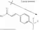


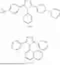


Sources:
- United States Patent and Trademark Office - verify current appl. status at the USPTO↗
Similar patent applications:
- » 20240317599
METAL OXIDE NANOPARTICLE, NANOCOMPOSITE INCLUDING THE METAL OXIDE NANOPARTICLE, AND INK COMPOSITION, LIGHT-EMITTING DEVICE, ELECTRONIC APPARATUS, AND ELECTRONIC EQUIPMENT INCLUDING THE NANOCOMPOSITE - » 20240317601
METHOD OF MANUFACTURING METAL OXIDE NANOPARTICLES, METAL OXIDE NANOPARTICLES, AND INK COMPOSITION, LIGHT-EMITTING DEVICE, ELECTRONIC APPARATUS, AND ELECTRONIC DEVICE, EACH INCLUDING THE METAL OXIDE NANOPARTICLES
Recent applications in this class:
- » 20250171331 2025-05-29
METHOD OF PREPARING CATHODE ACTIVE MATERIAL PRECURSOR USING COUETTE-TAYLOR REACTORS - » 20220396498 2022-12-15
PROCESS FOR PRODUCING A SURFACE-MODIFIED PARTICULATE LITHIUM NICKEL METAL OXIDE MATERIAL - » 20210155501 2021-05-27
O3/P2 MIXED PHASE SODIUM-CONTAINING DOPED LAYERED OXIDE MATERIALS - » 20170174527 2017-06-22
Doped nickelate materials