Patent Applications published on Jul 26, 2012
Explore the 6,340 U.S. Patent Applications published on the 30th week of 2012, including 4,239 applications that subsequently received a Patent Grant.
Featured patent applications from Jul 26, 2012
US20120187179A1
Human necessities
Buttress film with hemostatic action for surgical stapling apparatus
A surgical stapling apparatus includes a jaw assembly including a pair of jaw members and a surgical buttress positioned adjacent a tissue contacting surface of at least one of the pair of jaw members. The surgical buttress includes a hemostatic agent and is configured to release the hemostatic agent therefrom upon actuation of the surgical stapling apparatus to approximate the pair of jaw members and exert a pressure on the surgical buttress.
Published: 2012-07-26US20120190386A1
Electricity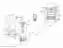
Wireless location establishing device
A system, method, service and wireless location-establishing device are disclosed, which locates its position by a plurality of means, including GPS satellite interrogation and triangulation. Alternative methods of location establishment include triangulating location data from nearby location-established objects such as WiFi or cell site towers, as well as from other present Invention location establishing devices (“Survey Eggs”). Once location has been established, the device can transmit and receive a variety of data based upon location, profile, and other factors, facilitating novel interactions and transactions.
Published: 2012-07-26 Assignee: The Invention Science Fund I, LLC.US20120190964A1
Human necessities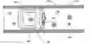
Vasculature and lymphatic system imaging and ablation
Devices, methods, and systems related to imaging and ablation are disclosed.
Published: 2012-07-26 Assignee: UChicago Argonne, LLC.US20120187305A1
Electricity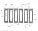
Microchannel plate detector and methods for their fabrication
A multi-component tunable resistive coating and methods of depositing the coating on the surfaces of a microchannel plate (MCP) detector. The resistive coating composed of a plurality of alternating layers of a metal oxide resistive component layer and a conductive component layer composed of at least one of a metal, a metal nitride and a metal sulfide. The coating may further include an emissive layer configured to produce a secondary electron emission in response to a particle interacting with the MCP and a neutron-absorbing layer configured to respond to a neutron interacting with the MCP.
Published: 2012-07-26 Assignee: Applied Materials, Inc..US20120190178A1
Electricity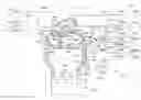
Polysilicon films by HDP-CVD
Methods of forming polysilicon layers are described. The methods include forming a high-density plasma from a silicon precursor in a substrate processing region containing the deposition substrate. The described methods produce polycrystalline films at reduced substrate temperature (e.g. <500° C.) relative to prior art techniques. The availability of a bias plasma power adjustment further enables adjustment of conformality of the formed polysilicon layer. When dopants are included in the high density plasma, they may be incorporated into the polysilicon layer in such a way that they do not require a separate activation step.
Published: 2012-07-26 Assignee: SCREEN HOLDINGS CO., LTD..US20120187083A1
Performing operations; transporting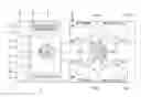
Substrate treatment method and substrate treatment apparatus
An inventive substrate treatment method includes a silylation step of supplying a silylation agent to a substrate, and an etching step of supplying an etching agent to the substrate after the silylation step. The method may further include a repeating step of repeating a sequence cycle including the silylation step and the etching step a plurality of times. The cycle may further include a rinsing step of supplying a rinse liquid to the substrate after the etching step. The cycle may further include a UV irradiation step of irradiating the substrate with ultraviolet radiation after the etching step. The method may further include a pre-silylation or post-silylation UV irradiation step of irradiating the substrate with the ultraviolet radiation before or after the silylation step.
Published: 2012-07-26 Assignee: ASM International N.V..US20120186573A1
Electricity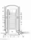
Thermal processing furnace and liner for the same
A thermal processing furnace, comprising: a generally bell jar-shaped outer reaction tube having a central axis; and an open-ended inner reaction tube for accommodating a wafer boat holding a plurality of substrates, which inner reaction tube is substantially coaxially disposed within the outer reaction tube, thereby defining a gas passage between an outer wall of the inner reaction tube and an inner wall of the outer reaction tube, wherein at least one of the outer wall of the inner reaction tube and the inner wall of the outer reaction tube is provided with a flow deflector that protrudes radially from the respective wall into the gas passage.
Published: 2012-07-26 Assignee: Applied Materials, Inc..US20120190185A1
Electricity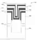
Plasma treatment of silicon nitride and silicon oxynitride
A method of forming a semiconductor device is disclosed. Nitrogen layers of an IPD stack are deposited using silane and a nitrogen plasma to yield a nitride layer plasma treated through its entire thickness. In addition to nitriding the bottom nitride layer of the stack, the middle nitride layer may also be nitrided. Depositing silicon from silane in a nitrogen plasma may be accomplished using high density plasma, ALD, or remote plasma processes. Elevated temperature may be used during deposition to reduce residual hydrogen in the deposited layer.
Published: 2012-07-26 Assignee: TAIWAN SEMICONDUCTOR MANUFACTURING COMPANY, LTD..US20120187486A1
Electricity
Non-uniform channel junction-less transistor
The present disclosure discloses a method of forming a semiconductor layer on a substrate. The method includes patterning the semiconductor layer into a fin structure. The method includes forming a gate dielectric layer and a gate electrode layer over the fin structure. The method includes patterning the gate dielectric layer and the gate electrode layer to form a gate structure in a manner so that the gate structure wraps around a portion of the fin structure. The method includes performing a plurality of implantation processes to form source/drain regions in the fin structure. The plurality of implantation processes are carried out in a manner so that a doping profile across the fin structure is non-uniform, and a first region of the portion of the fin structure that is wrapped around by the gate structure has a lower doping concentration level than other regions of the fin structure.
Published: 2012-07-26US20120191900A1
Physics
MEMORY MANAGEMENT DEVICE
A memory management device of an example of the invention controls writing into and reading from a main memory including a nonvolatile semiconductor memory and a volatile semiconductor memory in response to a writing request and a reading request from a processor. The memory management device includes a coloring information storage unit that stores coloring information generated based on a data characteristic of write target data to be written into at least one of the nonvolatile semiconductor memory and the volatile semiconductor memory, and a writing management unit that references the coloring information to determines a region into which the write target data is written from the nonvolatile semiconductor memory and the volatile semiconductor memory.